Synthesis for Pass Transistor Logic Maciej Ciesielski Dept
![PTL Synthesis Flow [Yano 96] • Express Boolean logic as shared, multi-output BDD • PTL Synthesis Flow [Yano 96] • Express Boolean logic as shared, multi-output BDD •](https://slidetodoc.com/presentation_image/08588918902c95b2f34cefe72b0a8c53/image-27.jpg)
- Slides: 30

Synthesis for Pass Transistor Logic Maciej Ciesielski Dept. of Electrical & Computer Engineering University of Massachusetts, Amherst, USA ciesiel@ecs. umass. edu 2000 M. Ciesielski PTL Synthesis 1

Overview • Introduction – Pass transistor basics – Electrical considerations: margin, delay, power – Pass transistor logic (PTL) • Pass transistor logic synthesis – Based on conventional (CMOS) synthesis • Logic gates implemented in PTL – BDD-based synthesis • BDD mapping onto Y cells [Yano 96] • BDD decomposition + mapping onto CMOS and PTL (BDS system, [Yang 99] 2000 M. Ciesielski PTL Synthesis 2

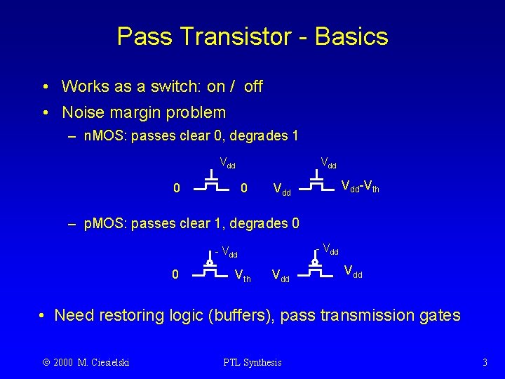
Pass Transistor - Basics • Works as a switch: on / off • Noise margin problem – n. MOS: passes clear 0, degrades 1 Vdd 0 Vdd-Vth Vdd – p. MOS: passes clear 1, degrades 0 - Vdd 0 Vth Vdd • Need restoring logic (buffers), pass transmission gates 2000 M. Ciesielski PTL Synthesis 3

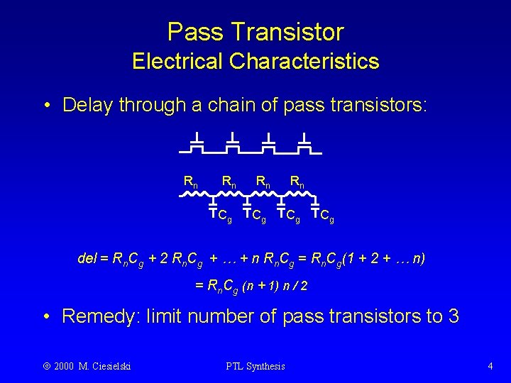
Pass Transistor Electrical Characteristics • Delay through a chain of pass transistors: Rn Rn Cg Cg del = Rn. Cg + 2 Rn. Cg + … + n Rn. Cg = Rn. Cg(1 + 2 + … n) = Rn. Cg (n + 1) n / 2 • Remedy: limit number of pass transistors to 3 2000 M. Ciesielski PTL Synthesis 4

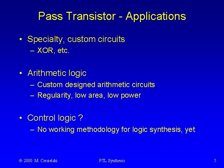
Pass Transistor - Applications • Specialty, custom circuits – XOR, etc. • Arithmetic logic – Custom designed arithmetic circuits – Regularity, low area, low power • Control logic ? – No working methodology for logic synthesis, yet 2000 M. Ciesielski PTL Synthesis 5

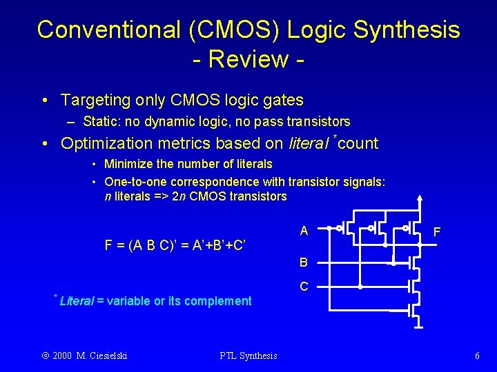
Conventional (CMOS) Logic Synthesis - Review • Targeting only CMOS logic gates – Static: no dynamic logic, no pass transistors • Optimization metrics based on literal *count • Minimize the number of literals • One-to-one correspondence with transistor signals: n literals => 2 n CMOS transistors F = (A B C)’ = A’+B’+C’ A F B * Literal C = variable or its complement 2000 M. Ciesielski PTL Synthesis 6

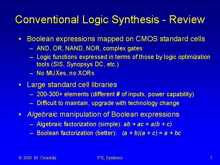
Conventional Logic Synthesis - Review • Boolean expressions mapped on CMOS standard cells – AND, OR, NAND, NOR, complex gates – Logic functions expressed in terms of those by logic optimization tools (SIS, Synopsys DC, etc. ) – No MUXes, no XORs • Large standard cell libraries – 200 -300+ elements (different # of inputs, power capability) – Difficult to maintain, upgrade with technology change • Algebraic manipulation of Boolean expressions – Algebraic factorization (simple): ab + ac = a(b + c) – Boolean factorization (better): (a + b)(a + c) = a + bc 2000 M. Ciesielski PTL Synthesis 7

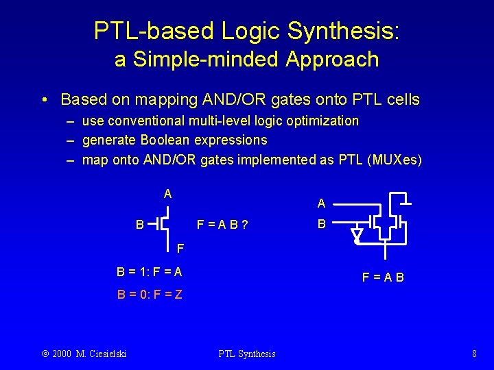
PTL-based Logic Synthesis: a Simple-minded Approach • Based on mapping AND/OR gates onto PTL cells – use conventional multi-level logic optimization – generate Boolean expressions – map onto AND/OR gates implemented as PTL (MUXes) A A F=AB? B B F B = 1: F = A F=AB B = 0: F = Z 2000 M. Ciesielski PTL Synthesis 8

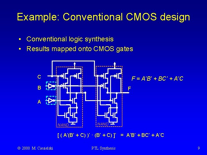
Example: Conventional CMOS design • Conventional logic synthesis • Results mapped onto CMOS gates C F = A’B’ + BC’ + A’C B F A NAND [ ( A’(B’ + C) )’ · (B’ + C) ]’ = A’B’ + BC’ + A’C 2000 M. Ciesielski PTL Synthesis 9

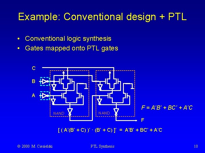
Example: Conventional design + PTL • Conventional logic synthesis • Gates mapped onto PTL gates C B A NAND F = A’B’ + BC’ + A’C F [ ( A’(B’ + C) )’ · (B’ + C) ]’ = A’B’ + BC’ + A’C 2000 M. Ciesielski PTL Synthesis 10

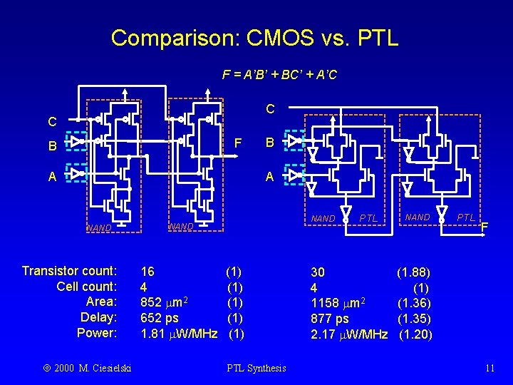
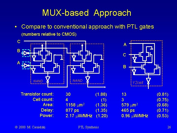
Comparison: CMOS vs. PTL F = A’B’ + BC’ + A’C C C F B B A A NAND Transistor count: Cell count: Area: Delay: Power: 2000 M. Ciesielski NAND 16 4 852 m 2 652 ps 1. 81 W/MHz (1) (1) (1) PTL Synthesis PTL 30 4 1158 m 2 877 ps 2. 17 W/MHz NAND PTL F (1. 88) (1. 36) (1. 35) (1. 20) 11

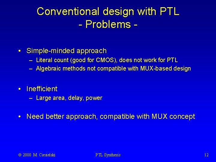
Conventional design with PTL - Problems • Simple-minded approach – Literal count (good for CMOS), does not work for PTL – Algebraic methods not compatible with MUX-based design • Inefficient – Large area, delay, power • Need better approach, compatible with MUX concept 2000 M. Ciesielski PTL Synthesis 12

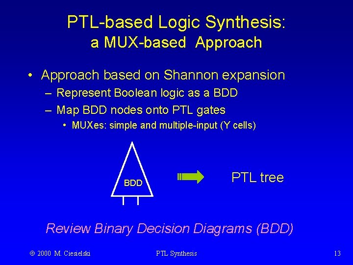
PTL-based Logic Synthesis: a MUX-based Approach • Approach based on Shannon expansion – Represent Boolean logic as a BDD – Map BDD nodes onto PTL gates • MUXes: simple and multiple-input (Y cells) PTL tree BDD Review Binary Decision Diagrams (BDD) 2000 M. Ciesielski PTL Synthesis 13

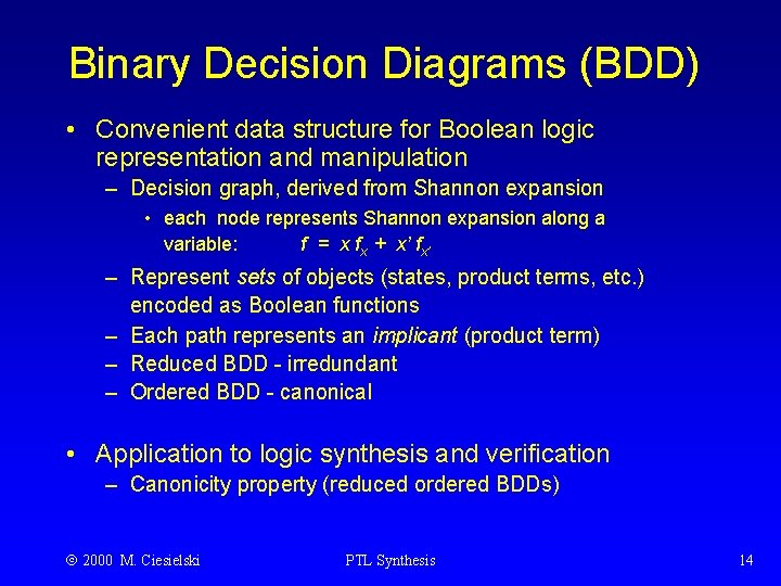
Binary Decision Diagrams (BDD) • Convenient data structure for Boolean logic representation and manipulation – Decision graph, derived from Shannon expansion • each node represents Shannon expansion along a variable: f = x fx + x’ fx’ – Represent sets of objects (states, product terms, etc. ) encoded as Boolean functions – Each path represents an implicant (product term) – Reduced BDD - irredundant – Ordered BDD - canonical • Application to logic synthesis and verification – Canonicity property (reduced ordered BDDs) 2000 M. Ciesielski PTL Synthesis 14

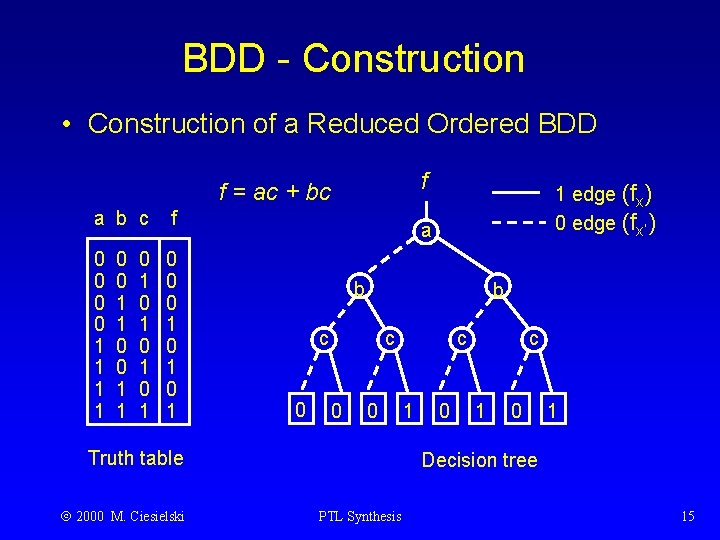
BDD - Construction • Construction of a Reduced Ordered BDD f f = ac + bc a b c f 0 0 1 1 0 0 0 1 0 1 0 0 1 1 0 1 0 1 a b b c 0 0 Truth table 2000 M. Ciesielski 1 edge (fx) 0 edge (fx’) c 1 0 1 Decision tree PTL Synthesis 15

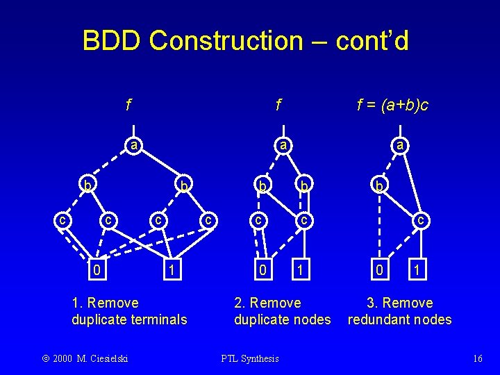
BDD Construction – cont’d f f a a b b b c c 0 c c 1 1. Remove duplicate terminals 2000 M. Ciesielski f = (a+b)c c 0 a b c 1 2. Remove duplicate nodes PTL Synthesis b c 0 1 3. Remove redundant nodes 16

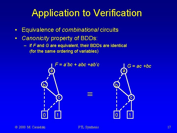
Application to Verification • Equivalence of combinational circuits • Canonicity property of BDDs: – if F and G are equivalent, their BDDs are identical (for the same ordering of variables) F = a’bc + abc +ab’c a a b c 0 2000 M. Ciesielski 1 b c 0 PTL Synthesis G = ac +bc 1 17

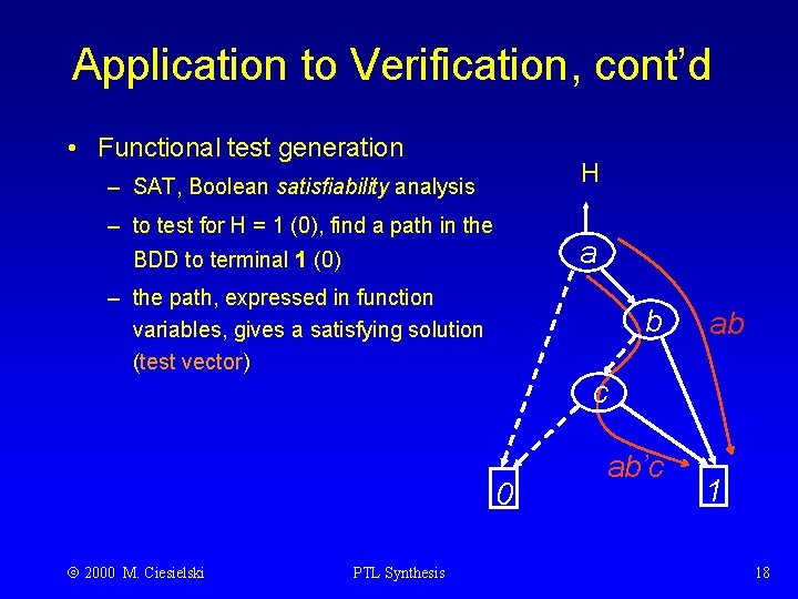
Application to Verification, cont’d • Functional test generation H – SAT, Boolean satisfiability analysis – to test for H = 1 (0), find a path in the a BDD to terminal 1 (0) – the path, expressed in function variables, gives a satisfying solution (test vector) b ab c 0 2000 M. Ciesielski PTL Synthesis ab’c 1 18

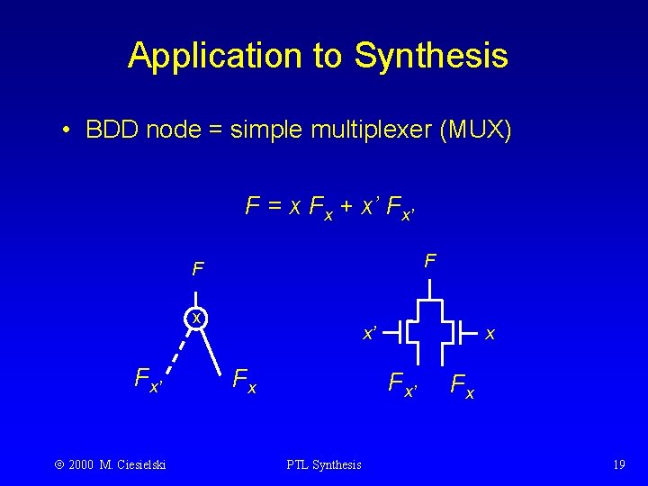
Application to Synthesis • BDD node = simple multiplexer (MUX) F = x Fx + x’ F F x Fx’ 2000 M. Ciesielski x’ Fx x Fx’ PTL Synthesis Fx 19

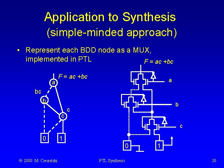
Application to Synthesis (simple-minded approach) • Represent each BDD node as a MUX, implemented in PTL F = ac +bc a bc b c c 0 1 0 2000 M. Ciesielski PTL Synthesis 1 20

PTL-based Logic Synthesis - Problems • Ineffective for larger circuits – – too large, too slow, too many MUXes pass transistor chains are too long need separating buffers need methodology for synthesizing circuits from their BDDs 2000 M. Ciesielski PTL Synthesis 21

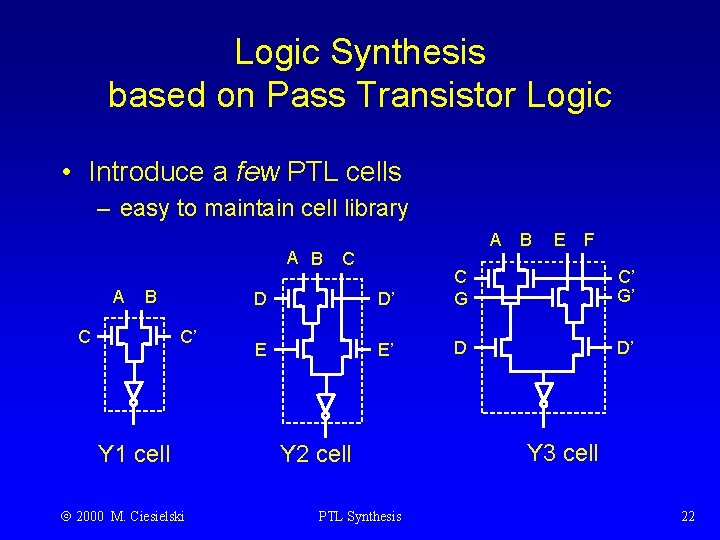
Logic Synthesis based on Pass Transistor Logic • Introduce a few PTL cells – easy to maintain cell library A B C C’ Y 1 cell 2000 M. Ciesielski A C D D’ C G E E’ D Y 2 cell PTL Synthesis B E F C’ G’ D’ Y 3 cell 22

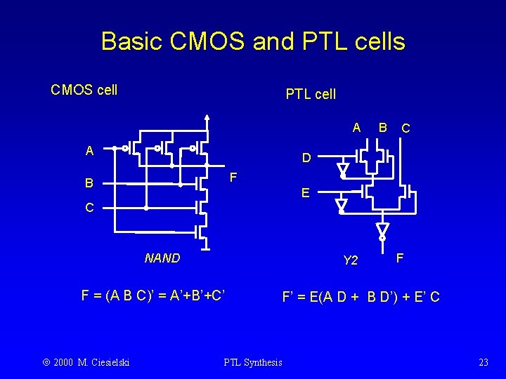
Basic CMOS and PTL cells CMOS cell PTL cell A A B C D F B E C NAND Y 2 F = (A B C)’ = A’+B’+C’ 2000 M. Ciesielski F F’ = E(A D + B D’) + E’ C PTL Synthesis 23

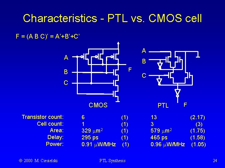
Characteristics - PTL vs. CMOS cell F = (A B C)’ = A’+B’+C’ A A B F B C C CMOS Transistor count: Cell count: Area: Delay: Power: 2000 M. Ciesielski 6 1 329 m 2 295 ps 0. 91 W/MHz PTL (1) (1) (1) PTL Synthesis F 13 (2. 17) 3 (3) 579 m 2 (1. 75) 465 ps (1. 58) 0. 96 W/MHz (1. 05) 24

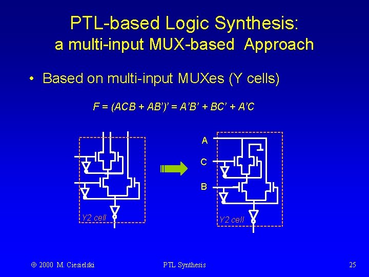
PTL-based Logic Synthesis: a multi-input MUX-based Approach • Based on multi-input MUXes (Y cells) F = (ACB + AB’)’ = A’B’ + BC’ + A’C A C B Y 2 cell 2000 M. Ciesielski Y 2 cell PTL Synthesis 25

MUX-based Approach • Compare to conventional approach with PTL gates (numbers relative to CMOS) C A B NAND Transistor count: Cell count: Area: Delay: Power: 2000 M. Ciesielski NAND 30 4 1158 m 2 877 ps 2. 17 W/MHz Y 2 cell (1. 88) (1. 36) (1. 35) (1. 20) PTL Synthesis 13 3 579 m 2 465 ps 0. 96 W/MHz (0. 81) (0. 75) (0. 68) (0. 71) (0. 53) 26
![PTL Synthesis Flow Yano 96 Express Boolean logic as shared multioutput BDD PTL Synthesis Flow [Yano 96] • Express Boolean logic as shared, multi-output BDD •](https://slidetodoc.com/presentation_image/08588918902c95b2f34cefe72b0a8c53/image-27.jpg)
PTL Synthesis Flow [Yano 96] • Express Boolean logic as shared, multi-output BDD • Partition BDD into smaller sub-trees, isomorphic with Y cells • Map each sub-tree onto a Y cell • Insert buffers at the Y-cell boundaries • this keeps pass transistor chains limited to 2 (Y tree height) • Fix circuit polarity by propagating inverters • Adjust inverter power (P 2, 4, etc) according to cell load 2000 M. Ciesielski PTL Synthesis 27

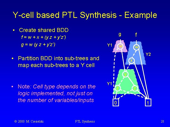
Y-cell based PTL Synthesis - Example • Create shared BDD f = w + x + (y z + y’z’) g = w (y z + y’z’) Y 1 g f w w Y 2 • Partition BDD into sub-trees and map each sub-trees to a Y cell x y • Note: Cell type depends on the logic implemented, not just on the number of variables/inputs 2000 M. Ciesielski PTL Synthesis Y 1 z 0 z 1 28

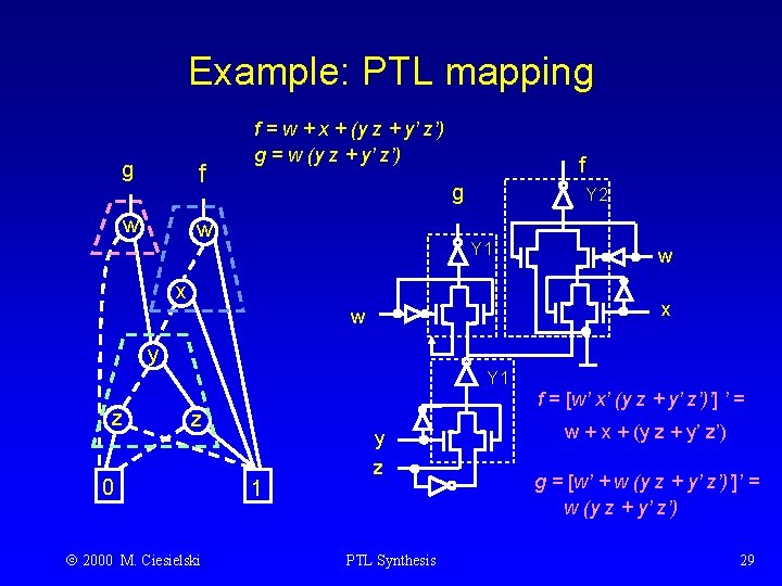
Example: PTL mapping g f w f = w + x + (y z + y’ z’) g = w (y z + y’ z’) f g w Y 2 Y 1 x w y Y 1 z f = [w’ x’ (y z + y’ z’)’] ’ = z 0 2000 M. Ciesielski y 1 z PTL Synthesis w + x + (y z + y’ z’) g = [w’ + w (y z + y’ z’)’]’ = w (y z + y’ z’) 29

PTL Synthesis - Results • Impressive results for control logic and arithmetic circuits – improvement in area, delay and power ! – need BDD synthesis & partitioning methodology – use CMOS gates as natural buffers? • New research (BDS) – mixing CMOS with PTL 2000 M. Ciesielski PTL Synthesis 30