Research on Interconnect ChungKuan Cheng University of California
- Slides: 23

Research on Interconnect Chung-Kuan Cheng University of California, San Diego ckcheng@ucsd. edu

Research on Interconnect • Physical Layout – 3 D Floorplanning, Placement, Bus Topology • Whole Chip Analysis – Interconnect Dominance – Parallel SPICE (1): circuit theory, numerical methods, implementation • Signal Interconnects – Power, Throughput, Latency – EM Waves, e. g. T Line (2): eye diagram analysis • Power Ground Distribution Networks – Stimuli, Networks, Noise (3) – 3 D ICs (4): worst case analysis 2

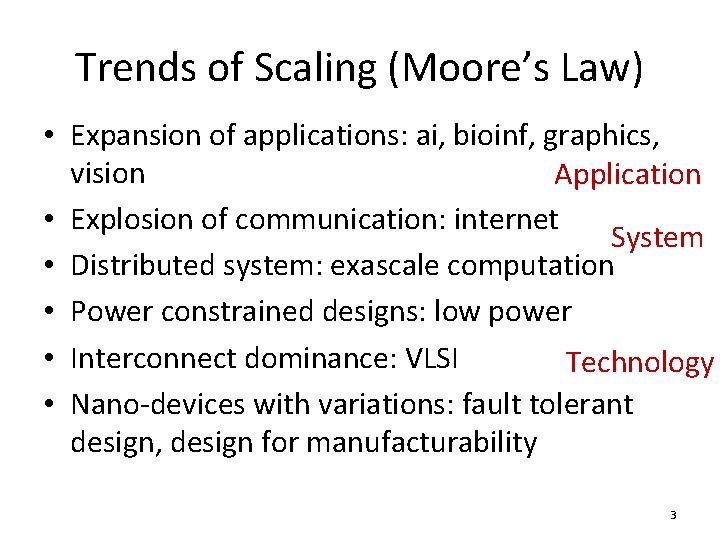
Trends of Scaling (Moore’s Law) • Expansion of applications: ai, bioinf, graphics, vision Application • Explosion of communication: internet System • Distributed system: exascale computation • Power constrained designs: low power • Interconnect dominance: VLSI Technology • Nano-devices with variations: fault tolerant design, design for manufacturability 3

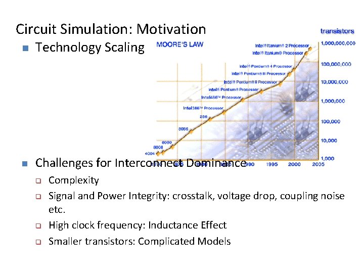
Circuit Simulation: Motivation n Technology Scaling n Challenges for Interconnect Dominance q q Complexity Signal and Power Integrity: crosstalk, voltage drop, coupling noise etc. High clock frequency: Inductance Effect Smaller transistors: Complicated Models

Parallel SPICE • Transient Analysis for Whole System • Acknowledgement: NSF • Researchers: F. J. Liu, X. D. Yang, Z. Qin, Z. Zhu, R. Shi, H. Peng, S. H. Weng, Q. Chen, Y. Shen 5

SPICE Research Outline • • Cluster Machines Netlist Partitioning Whole Chip Analysis SPICE Accuracy 6

Simulation: Goal • Analyze whole chip with 100 x memory capacity, 100 x speed up, 100 x efficiency for designers • Set standard of input/output for parallel processing • Allow cluster machines or cloud computing for the acceleration • Demonstrate the results via power ground analysis and tera Hertz circuitry 7

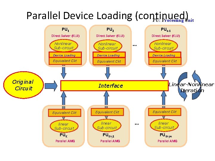
Parallel Device Loading (continued) PU: Processing Unit PU 1 PU 2 PUk-1 Direct Solver (KLU) … Nonlinear Sub-circuit Device Loading Equivalent Ckt Original Circuit Linear-Nonlinear Iteration Interface Equivalent Ckt linear Sub-circuit PUK Parallel AMG PUK+j 1 Parallel AMG Nonlinear Sub-circuit Equivalent Ckt … linear Sub-circuit PUK+jm Parallel AMG

Action Items • Input/Output Parsing and • Screening • – Parallel Input – Netlist Transformation • – Parallel Output • Device Evaluation – Transistor Model • Integration – Stability – Stiffness Handling • Sensitivity Calculation Adaptive Time Step Control Parallelization Overall Framework – Implement in C/C++ – Which math library? – Sparse matrix library? – Parallel Implementation 9

Remarks • Scalable Parallel Processing – Integration – Matrix Operations • Applications – Power Ground Network Analysis – Substrate Noises – Memory Analysis – Tera Hertz Circuit Simulation 10

Signal Interconnect • • Introduction Contributions On-Chip T Lines Conclusion 11 12/30/2021

Signal Interconnect • Goals: – Power – Throughput – Latency • Technology – Scaling Effect – On-Chip Interconnect – Chip to Chip – 3 D ICs 12 12/30/2021

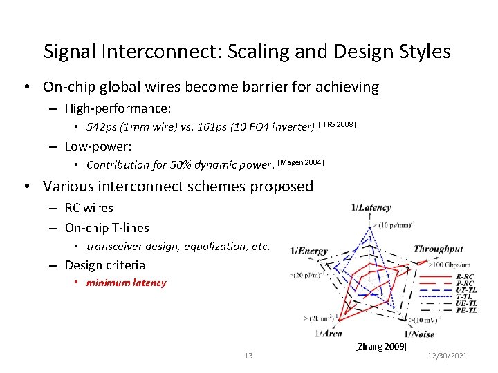
Signal Interconnect: Scaling and Design Styles • On-chip global wires become barrier for achieving – High-performance: • 542 ps (1 mm wire) vs. 161 ps (10 FO 4 inverter) [ITRS 2008] – Low-power: • Contribution for 50% dynamic power. [Magen 2004] • Various interconnect schemes proposed – RC wires – On-chip T-lines • transceiver design, equalization, etc. – Design criteria • minimum latency 13 [Zhang 2009] 12/30/2021

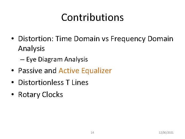
Contributions • Distortion: Time Domain vs Frequency Domain Analysis – Eye Diagram Analysis • Passive and Active Equalizer • Distortionless T Lines • Rotary Clocks 14 12/30/2021

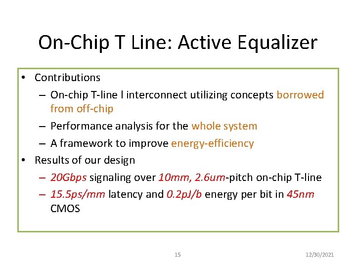
On-Chip T Line: Active Equalizer • Contributions – On-chip T-line l interconnect utilizing concepts borrowed from off-chip – Performance analysis for the whole system – A framework to improve energy-efficiency • Results of our design – 20 Gbps signaling over 10 mm, 2. 6 um-pitch on-chip T-line – 15. 5 ps/mm latency and 0. 2 p. J/b energy per bit in 45 nm CMOS 15 12/30/2021

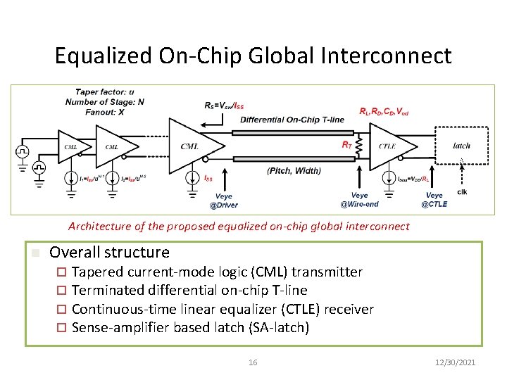
Equalized On-Chip Global Interconnect Architecture of the proposed equalized on-chip global interconnect n Overall structure ¨ ¨ Tapered current-mode logic (CML) transmitter Terminated differential on-chip T-line Continuous-time linear equalizer (CTLE) receiver Sense-amplifier based latch (SA-latch) 16 12/30/2021

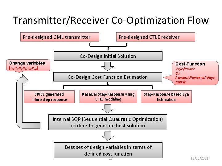
Transmitter/Receiver Co-Optimization Flow Pre-designed CML transmitter Pre-designed CTLE receiver Co-Design Initial Solution Change variables Cost-Function [ISS, RT, RL, RD, CD, Vod] Co-Design Cost Function Estimation SPICE generated T-line step response Receiver Step-Response using CTLE modeling Veye/Power Or Lowest Power w/ Veye const. Step-Response Based Eye Estimation Internal SQP (Sequential Quadratic Optimization) routine to generate best solution Best set of design variables in terms of defined cost function 17 12/30/2021

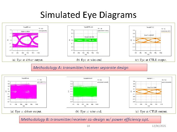
Simulated Eye Diagrams Methodology A: transmitter/receiver separate design Methodology B: transmitter/receiver co-design w/ power efficiency opt. 18 12/30/2021

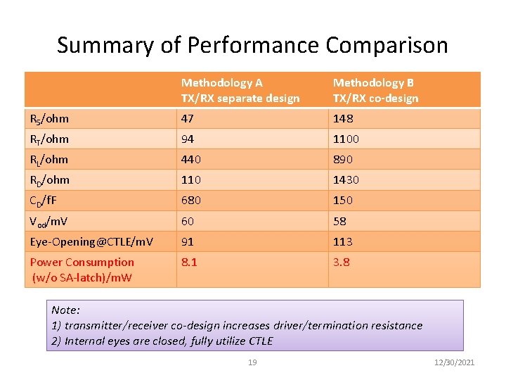
Summary of Performance Comparison Methodology A TX/RX separate design Methodology B TX/RX co-design RS/ohm 47 148 RT/ohm 94 1100 RL/ohm 440 890 RD/ohm 110 1430 CD/f. F 680 150 Vod/m. V 60 58 Eye-Opening@CTLE/m. V 91 113 Power Consumption (w/o SA-latch)/m. W 8. 1 3. 8 Note: 1) transmitter/receiver co-design increases driver/termination resistance 2) Internal eyes are closed, fully utilize CTLE 19 12/30/2021

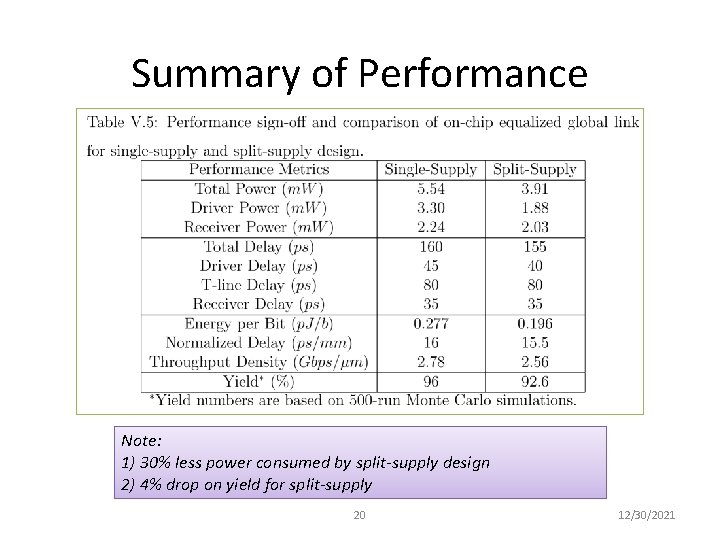
Summary of Performance Note: 1) 30% less power consumed by split-supply design 2) 4% drop on yield for split-supply 20 12/30/2021

Remarks • Interconnect for 3 D ICs – TSVs – Interposer • Analysis – Eye Diagram vs Power Ground Noises 21 12/30/2021

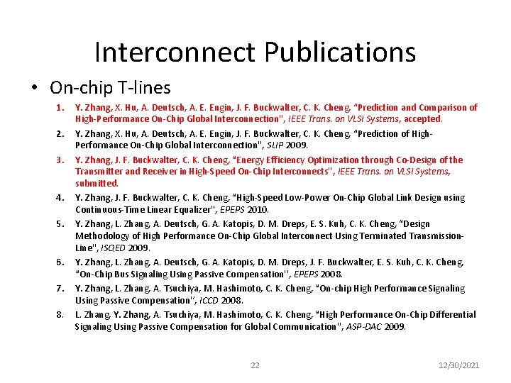
Interconnect Publications • On-chip T-lines 1. 2. 3. 4. 5. 6. 7. 8. Y. Zhang, X. Hu, A. Deutsch, A. E. Engin, J. F. Buckwalter, C. K. Cheng, “Prediction and Comparison of High-Performance On-Chip Global Interconnection'', IEEE Trans. on VLSI Systems, accepted. Y. Zhang, X. Hu, A. Deutsch, A. E. Engin, J. F. Buckwalter, C. K. Cheng, “Prediction of High. Performance On-Chip Global Interconnection'', SLIP 2009. Y. Zhang, J. F. Buckwalter, C. K. Cheng, “Energy Efficiency Optimization through Co-Design of the Transmitter and Receiver in High-Speed On-Chip Interconnects'', IEEE Trans. on VLSI Systems, submitted. Y. Zhang, J. F. Buckwalter, C. K. Cheng, “High-Speed Low-Power On-Chip Global Link Design using Continuous-Time Linear Equalizer'', EPEPS 2010. Y. Zhang, L. Zhang, A. Deutsch, G. A. Katopis, D. M. Dreps, E. S. Kuh, C. K. Cheng, “Design Methodology of High Performance On-Chip Global Interconnect Using Terminated Transmission. Line'', ISQED 2009. Y. Zhang, L. Zhang, A. Deutsch, G. A. Katopis, D. M. Dreps, J. F. Buckwalter, E. S. Kuh, C. K. Cheng, “On-Chip Bus Signaling Using Passive Compensation'', EPEPS 2008. Y. Zhang, L. Zhang, A. Tsuchiya, M. Hashimoto, C. K. Cheng, “On-chip High Performance Signaling Using Passive Compensation'‘, ICCD 2008. L. Zhang, Y. Zhang, A. Tsuchiya, M. Hashimoto, C. K. Cheng, “High Performance On-Chip Differential Signaling Using Passive Compensation for Global Communication'', ASP-DAC 2009. 22 12/30/2021

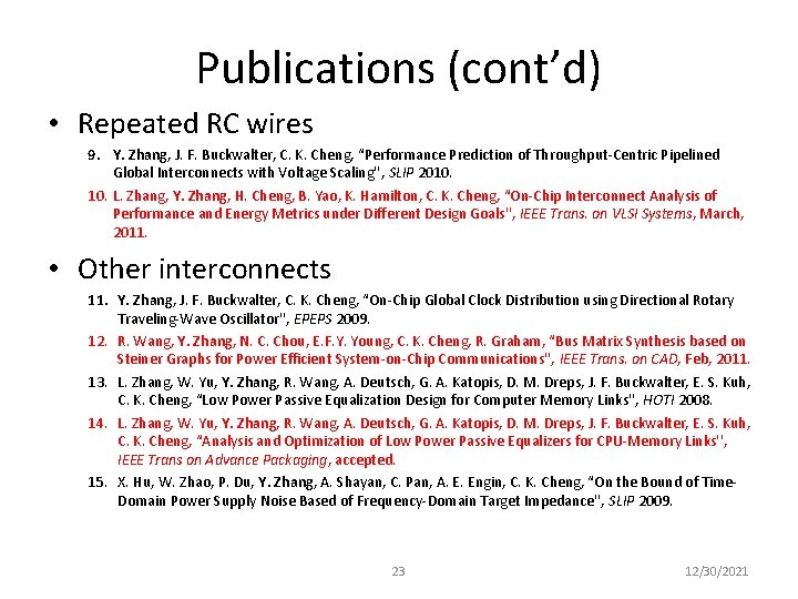
Publications (cont’d) • Repeated RC wires 9. Y. Zhang, J. F. Buckwalter, C. K. Cheng, “Performance Prediction of Throughput-Centric Pipelined Global Interconnects with Voltage Scaling'', SLIP 2010. L. Zhang, Y. Zhang, H. Cheng, B. Yao, K. Hamilton, C. K. Cheng, “On-Chip Interconnect Analysis of Performance and Energy Metrics under Different Design Goals'', IEEE Trans. on VLSI Systems, March, 2011. • Other interconnects 11. Y. Zhang, J. F. Buckwalter, C. K. Cheng, “On-Chip Global Clock Distribution using Directional Rotary Traveling-Wave Oscillator'', EPEPS 2009. 12. R. Wang, Y. Zhang, N. C. Chou, E. F. Y. Young, C. K. Cheng, R. Graham, “Bus Matrix Synthesis based on Steiner Graphs for Power Efficient System-on-Chip Communications'', IEEE Trans. on CAD, Feb, 2011. 13. L. Zhang, W. Yu, Y. Zhang, R. Wang, A. Deutsch, G. A. Katopis, D. M. Dreps, J. F. Buckwalter, E. S. Kuh, C. K. Cheng, “Low Power Passive Equalization Design for Computer Memory Links'', HOTI 2008. 14. L. Zhang, W. Yu, Y. Zhang, R. Wang, A. Deutsch, G. A. Katopis, D. M. Dreps, J. F. Buckwalter, E. S. Kuh, C. K. Cheng, “Analysis and Optimization of Low Power Passive Equalizers for CPU-Memory Links'', IEEE Trans on Advance Packaging, accepted. 15. X. Hu, W. Zhao, P. Du, Y. Zhang, A. Shayan, C. Pan, A. E. Engin, C. K. Cheng, “On the Bound of Time. Domain Power Supply Noise Based of Frequency-Domain Target Impedance'', SLIP 2009. 23 12/30/2021