Passive Distortion Compensation for Package Level Interconnect ChungKuan

- Slides: 37

Passive Distortion Compensation for Package Level Interconnect Chung-Kuan Cheng Dongsheng Ma & Janet Wang Univ. of Arizona UC San Diego 1

Outline 1. Motivation 2. Review of High-Speed Serial Links 3. Passive Distortion Compensation 1. Theory 2. Implementation 3. Simulation Results 4. Power Management and System Integration 5. Research Direction 2

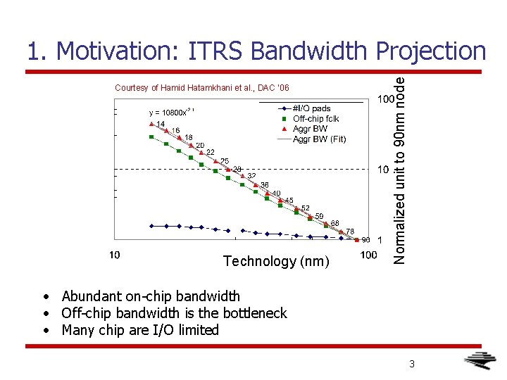
Courtesy of Hamid Hatamkhani et al. , DAC ‘ 06 Technology (nm) Normalized unit to 90 nm node 1. Motivation: ITRS Bandwidth Projection • Abundant on-chip bandwidth • Off-chip bandwidth is the bottleneck • Many chip are I/O limited 3

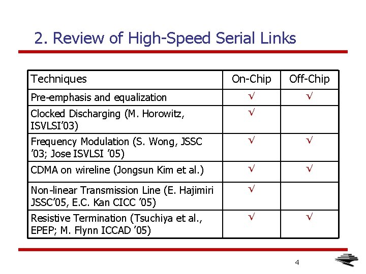
2. Review of High-Speed Serial Links Techniques On-Chip Off-Chip Pre-emphasis and equalization √ √ Clocked Discharging (M. Horowitz, ISVLSI’ 03) √ Frequency Modulation (S. Wong, JSSC ’ 03; Jose ISVLSI ’ 05) √ √ CDMA on wireline (Jongsun Kim et al. ) √ √ Non-linear Transmission Line (E. Hajimiri JSSC’ 05, E. C. Kan CICC ’ 05) √ Resistive Termination (Tsuchiya et al. , EPEP; M. Flynn ICCAD ’ 05) √ √ 4

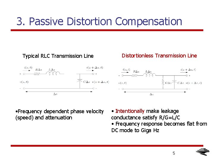
3. Passive Distortion Compensation Typical RLC Transmission Line • Frequency dependent phase velocity (speed) and attenuation Distortionless Transmission Line • Intentionally make leakage conductance satisfy R/G=L/C • Frequency response becomes flat from DC mode to Giga Hz 5

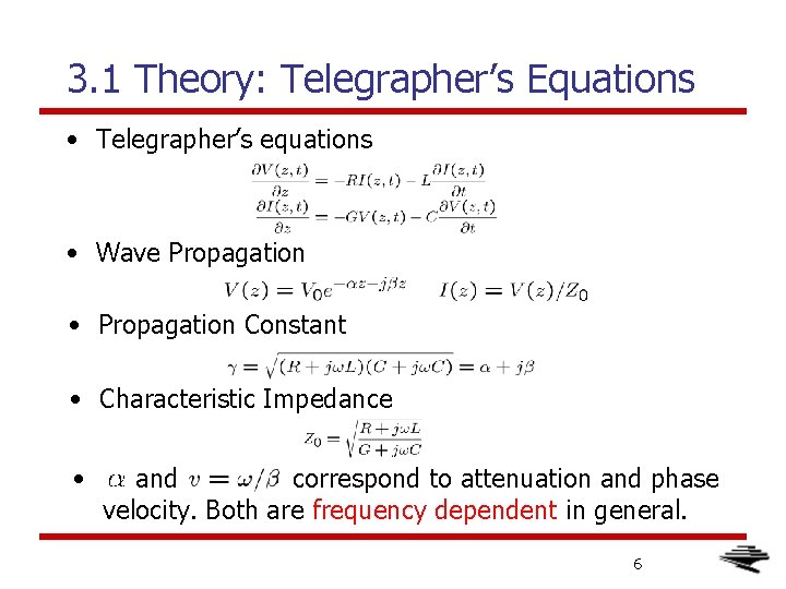
3. 1 Theory: Telegrapher’s Equations • Telegrapher’s equations • Wave Propagation • Propagation Constant • Characteristic Impedance • and correspond to attenuation and phase velocity. Both are frequency dependent in general. 6

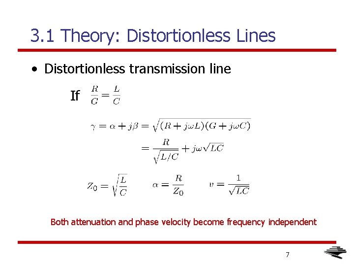
3. 1 Theory: Distortionless Lines • Distortionless transmission line If Both attenuation and phase velocity become frequency independent 7

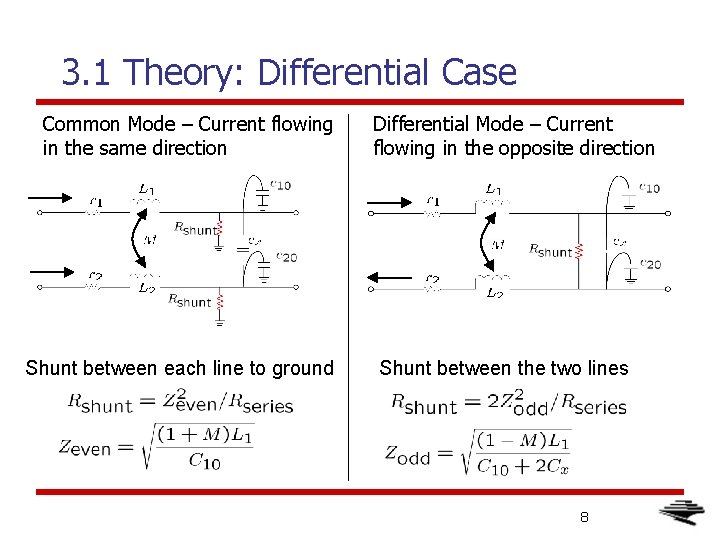
3. 1 Theory: Differential Case Common Mode – Current flowing in the same direction Shunt between each line to ground Differential Mode – Current flowing in the opposite direction Shunt between the two lines 8

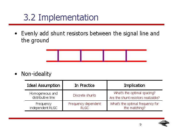
3. 2 Implementation • Evenly add shunt resistors between the signal line and the ground • Non-ideality Ideal Assumption In Practice Implication Homogeneous and distributive line Discrete shunts What’s the optimal spacing? Are the shunt resistors realizable? Frequency independent RLGC Frequency dependent RLGC What’s the optimal frequency for the matching? 9

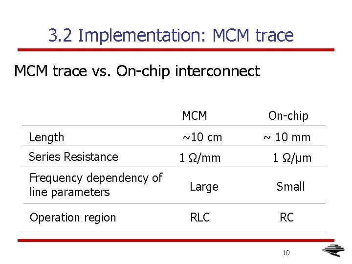
3. 2 Implementation: MCM trace vs. On-chip interconnect MCM Length Series Resistance On-chip ~10 cm ~ 10 mm 1 Ω/μm Frequency dependency of line parameters Large Small Operation region RLC RC 10

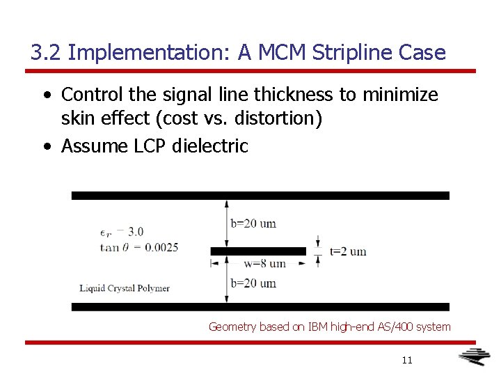
3. 2 Implementation: A MCM Stripline Case • Control the signal line thickness to minimize skin effect (cost vs. distortion) • Assume LCP dielectric Geometry based on IBM high-end AS/400 system 11

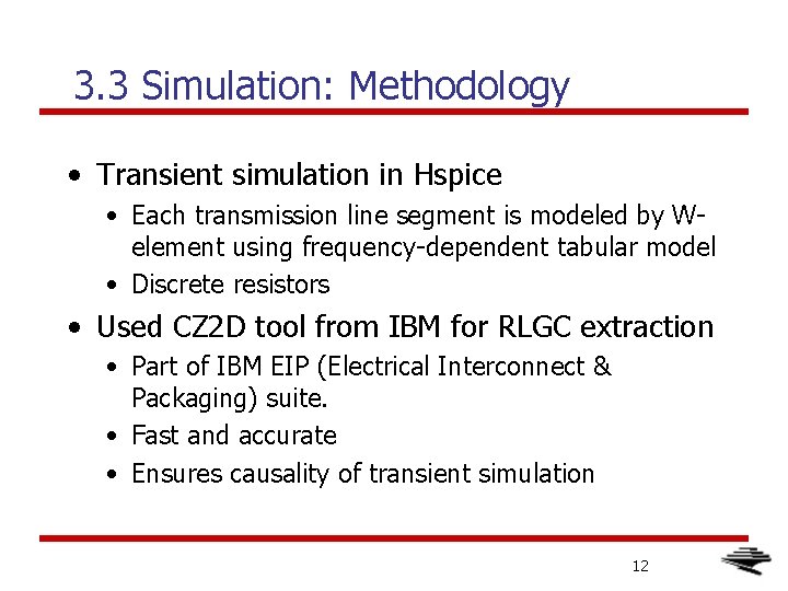
3. 3 Simulation: Methodology • Transient simulation in Hspice • Each transmission line segment is modeled by Welement using frequency-dependent tabular model • Discrete resistors • Used CZ 2 D tool from IBM for RLGC extraction • Part of IBM EIP (Electrical Interconnect & Packaging) suite. • Fast and accurate • Ensures causality of transient simulation 12

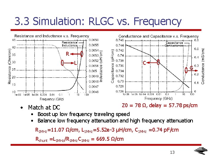
3. 3 Simulation: RLGC vs. Frequency R L • Match at DC C G Z 0 = 78 Ω, delay = 57. 78 ps/cm • Boost up low frequency traveling speed • Balance low frequency attenuation and high frequency attenuation R 1 MHz=11. 07 Ω/cm, L 1 MHz=5. 52 e-3 μH/cm, C 1 MHz =0. 74 p. F/cm Rshunt =L 1 MHz/R 1 MHz. C 1 MHz = 669. 5 Ω/cm 13

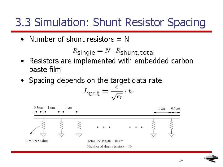
3. 3 Simulation: Shunt Resistor Spacing • Number of shunt resistors = N • Resistors are implemented with embedded carbon paste film • Spacing depends on the target data rate 14

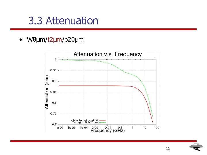
3. 3 Attenuation • W 8μm/t 2μm/b 20μm 15

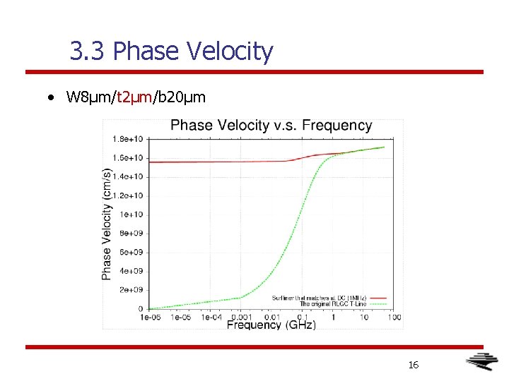
3. 3 Phase Velocity • W 8μm/t 2μm/b 20μm 16

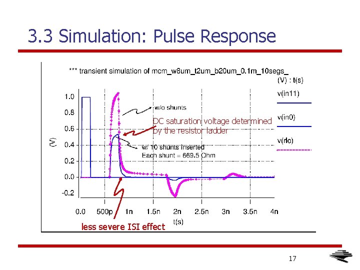
3. 3 Simulation: Pulse Response DC saturation voltage determined by the resistor ladder less severe ISI effect 17

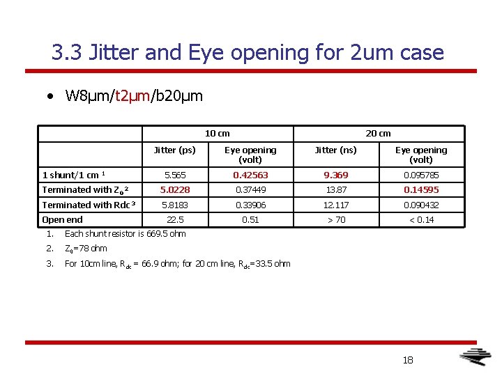
3. 3 Jitter and Eye opening for 2 um case • W 8μm/t 2μm/b 20μm 10 cm 20 cm Jitter (ps) Eye opening (volt) Jitter (ns) Eye opening (volt) 5. 565 0. 42563 9. 369 0. 095785 Terminated with Z 0 2 5. 0228 0. 37449 13. 87 0. 14595 Terminated with Rdc 3 5. 8183 0. 33906 12. 117 0. 090432 22. 5 0. 51 > 70 < 0. 14 1 shunt/1 cm 1 Open end 1. Each shunt resistor is 669. 5 ohm 2. Z 0=78 ohm 3. For 10 cm line, Rdc = 66. 9 ohm; for 20 cm line, Rdc=33. 5 ohm 18

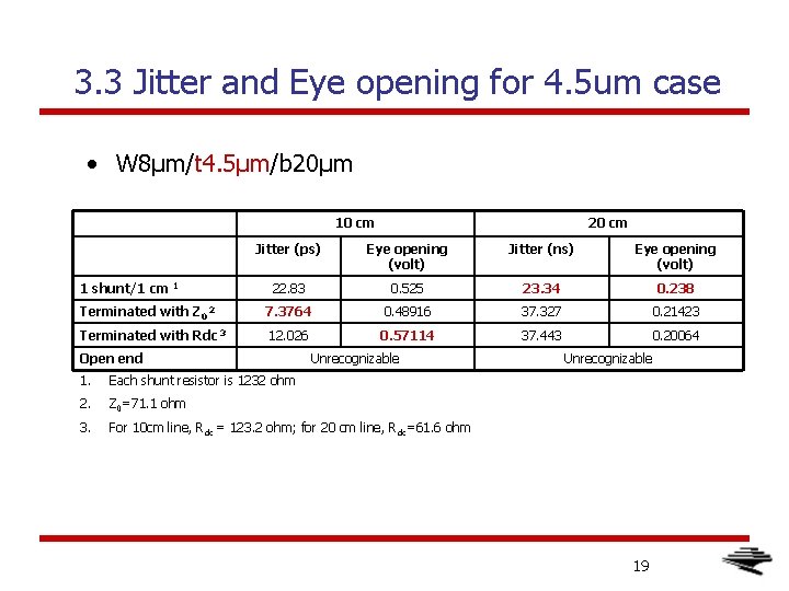
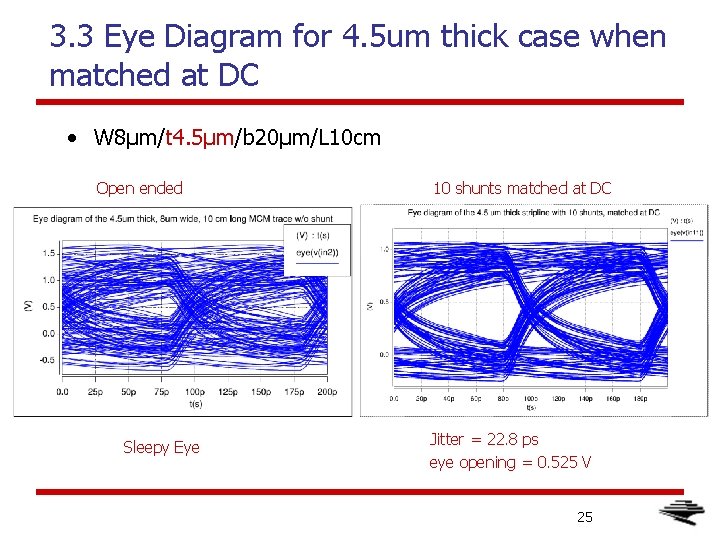
3. 3 Jitter and Eye opening for 4. 5 um case • W 8μm/t 4. 5μm/b 20μm 10 cm 20 cm Jitter (ps) Eye opening (volt) Jitter (ns) Eye opening (volt) 22. 83 0. 525 23. 34 0. 238 Terminated with Z 0 2 7. 3764 0. 48916 37. 327 0. 21423 Terminated with Rdc 3 12. 026 0. 57114 37. 443 0. 20064 1 shunt/1 cm 1 Open end Unrecognizable 1. Each shunt resistor is 1232 ohm 2. Z 0=71. 1 ohm 3. For 10 cm line, Rdc = 123. 2 ohm; for 20 cm line, Rdc=61. 6 ohm Unrecognizable 19

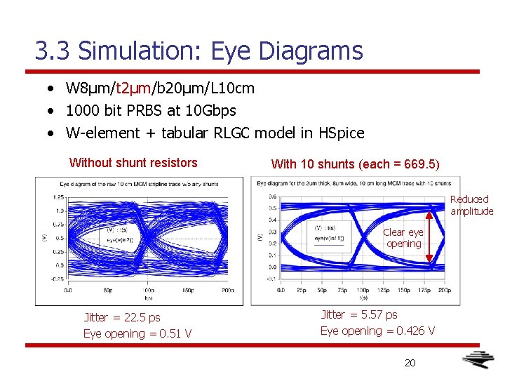
3. 3 Simulation: Eye Diagrams • W 8μm/t 2μm/b 20μm/L 10 cm • 1000 bit PRBS at 10 Gbps • W-element + tabular RLGC model in HSpice Without shunt resistors With 10 shunts (each = 669. 5) Reduced amplitude Clear eye opening Jitter = 22. 5 ps Eye opening = 0. 51 V Jitter = 5. 57 ps Eye opening = 0. 426 V 20

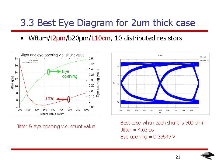
3. 3 Best Eye Diagram for 2 um thick case • W 8μm/t 2μm/b 20μm/L 10 cm, 10 distributed resistors Eye opening Jitter & eye opening v. s. shunt value Best case when each shunt is 500 ohm Jitter = 4. 63 ps Eye opening = 0. 35645 V 21

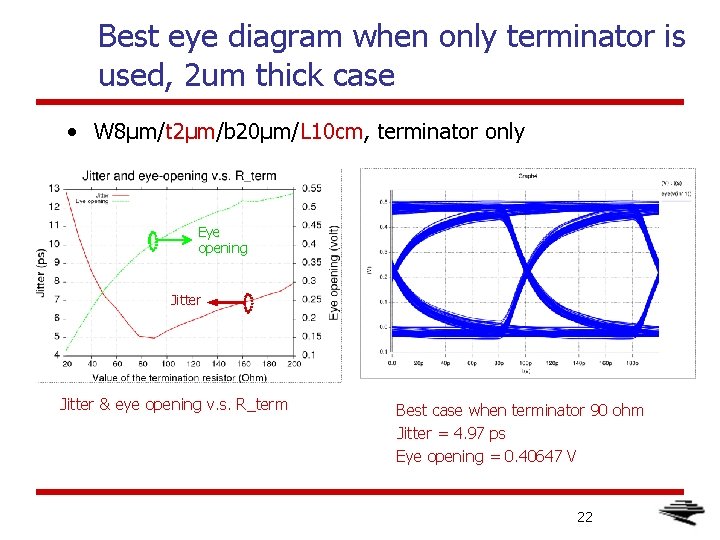
Best eye diagram when only terminator is used, 2 um thick case • W 8μm/t 2μm/b 20μm/L 10 cm, terminator only Eye opening Jitter & eye opening v. s. R_term Best case when terminator 90 ohm Jitter = 4. 97 ps Eye opening = 0. 40647 V 22

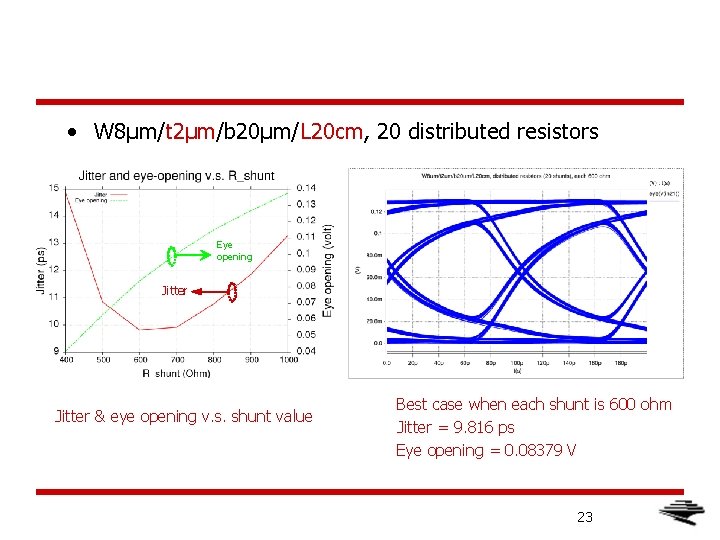
• W 8μm/t 2μm/b 20μm/L 20 cm, 20 distributed resistors Eye opening Jitter & eye opening v. s. shunt value Best case when each shunt is 600 ohm Jitter = 9. 816 ps Eye opening = 0. 08379 V 23

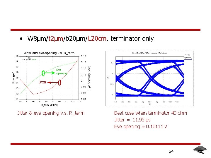
• W 8μm/t 2μm/b 20μm/L 20 cm, terminator only Eye opening Jitter & eye opening v. s. R_term Best case when terminator 40 ohm Jitter = 11. 95 ps Eye opening = 0. 10111 V 24

3. 3 Eye Diagram for 4. 5 um thick case when matched at DC • W 8μm/t 4. 5μm/b 20μm/L 10 cm Open ended Sleepy Eye 10 shunts matched at DC Jitter = 22. 8 ps eye opening = 0. 525 V 25

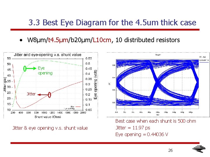
3. 3 Best Eye Diagram for the 4. 5 um thick case • W 8μm/t 4. 5μm/b 20μm/L 10 cm, 10 distributed resistors Eye opening Jitter & eye opening v. s. shunt value Best case when each shunt is 500 ohm Jitter = 11. 97 ps Eye opening = 0. 44036 V 26

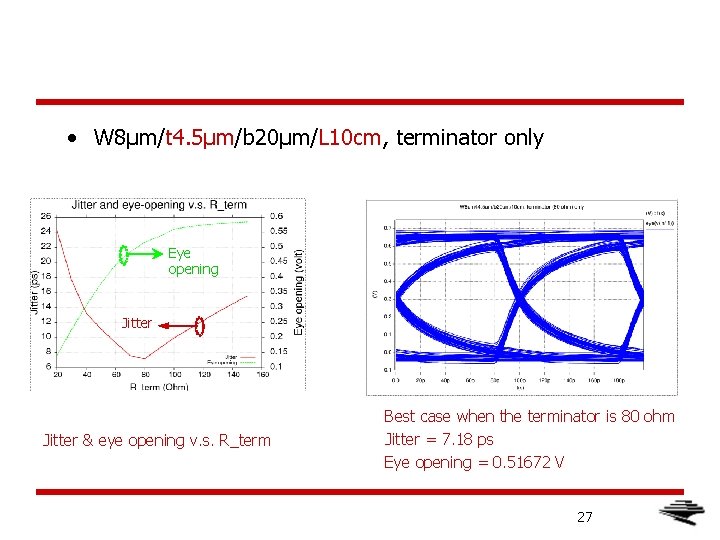
• W 8μm/t 4. 5μm/b 20μm/L 10 cm, terminator only Eye opening Jitter & eye opening v. s. R_term Best case when the terminator is 80 ohm Jitter = 7. 18 ps Eye opening = 0. 51672 V 27

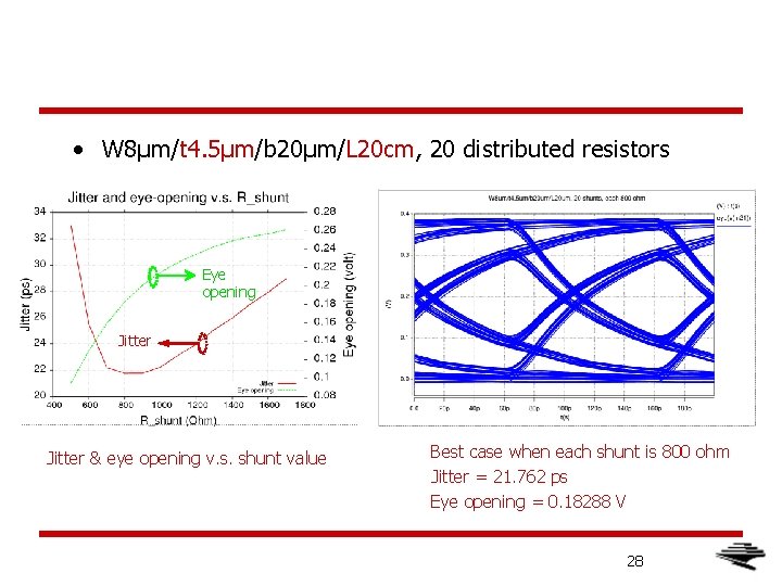
• W 8μm/t 4. 5μm/b 20μm/L 20 cm, 20 distributed resistors Eye opening Jitter & eye opening v. s. shunt value Best case when each shunt is 800 ohm Jitter = 21. 762 ps Eye opening = 0. 18288 V 28

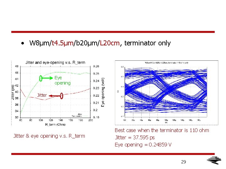
• W 8μm/t 4. 5μm/b 20μm/L 20 cm, terminator only Eye opening Jitter & eye opening v. s. R_term Best case when the terminator is 110 ohm Jitter = 37. 595 ps Eye opening = 0. 24859 V 29

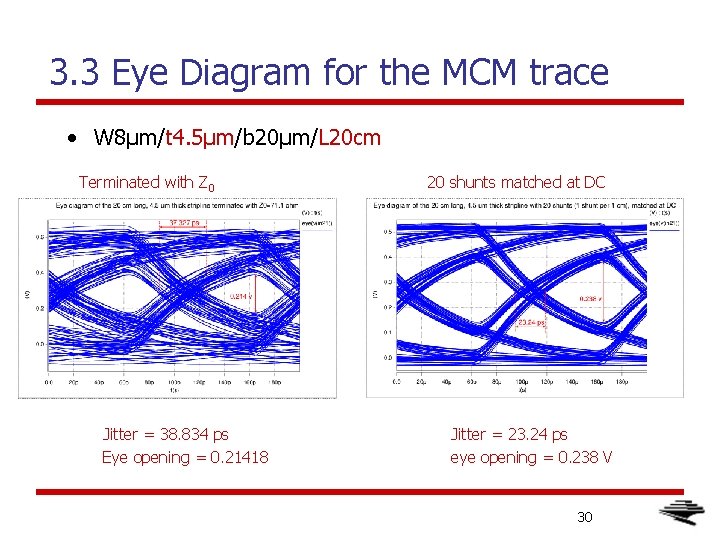
3. 3 Eye Diagram for the MCM trace • W 8μm/t 4. 5μm/b 20μm/L 20 cm Terminated with Z 0 Jitter = 38. 834 ps Eye opening = 0. 21418 20 shunts matched at DC Jitter = 23. 24 ps eye opening = 0. 238 V 30

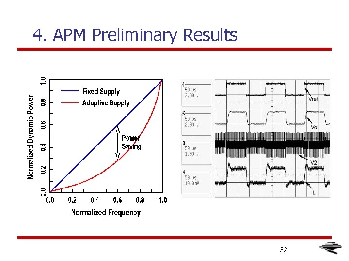
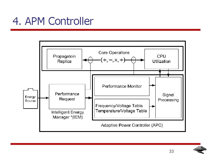
4. Adaptive Power Management (APM) • The distortionless signaling simplifies the interface circuitry. However, the twice heavier attenuation due to passive compensation calls for adaptive power management; • With adaptive power management, we adaptively regulate the power supply of the transmitter according to attenuation; • The regulated supply voltage guarantees the speed of transmission while keeping the minimal power overhead and well-controlled bit-error rate. 31

4. APM Preliminary Results 32

4. APM Controller 33

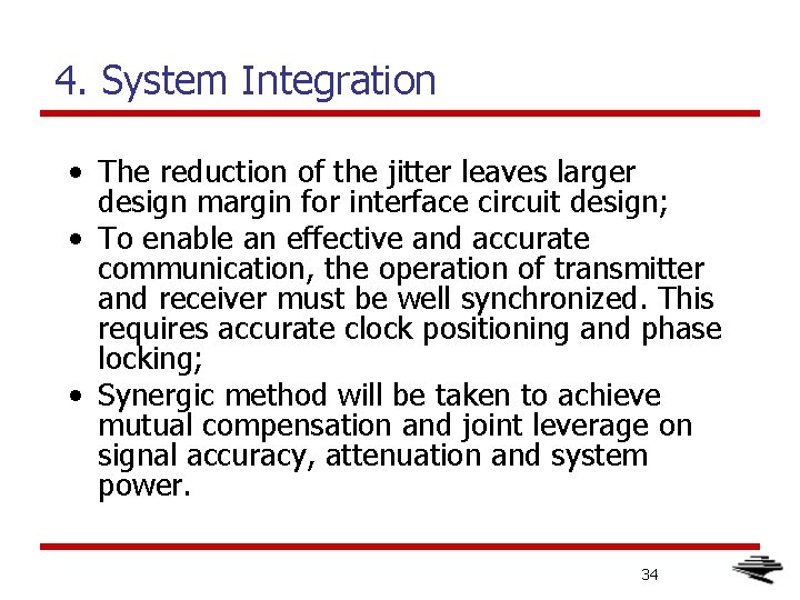
4. System Integration • The reduction of the jitter leaves larger design margin for interface circuit design; • To enable an effective and accurate communication, the operation of transmitter and receiver must be well synchronized. This requires accurate clock positioning and phase locking; • Synergic method will be taken to achieve mutual compensation and joint leverage on signal accuracy, attenuation and system power. 34

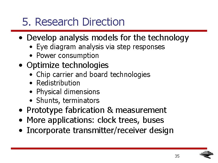
5. Research Direction • Develop analysis models for the technology • Eye diagram analysis via step responses • Power consumption • Optimize technologies • • Chip carrier and board technologies Redistribution Physical dimensions Shunts, terminators • Prototype fabrication & measurement • More applications: clock trees, buses • Incorporate transmitter/receiver design 35

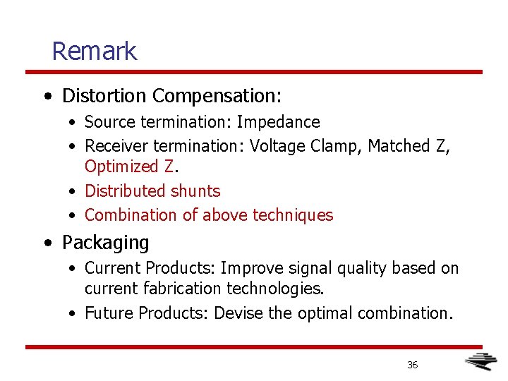
Remark • Distortion Compensation: • Source termination: Impedance • Receiver termination: Voltage Clamp, Matched Z, Optimized Z. • Distributed shunts • Combination of above techniques • Packaging • Current Products: Improve signal quality based on current fabrication technologies. • Future Products: Devise the optimal combination. 36

The End Thank you! 37