Phase shifter design for Macro Pixel ASIC Jian

- Slides: 22

Phase shifter design for Macro Pixel ASIC Jian Wang wangjian@ustc. edu. cn State Key Laboratory of Particle Detection and Electronics University of Science and Technology of China Southern Methodist University

Outline Background Interface Digital flow Phase shifter custom design for 320 MHz clock • Post-simulation results • Summary • •

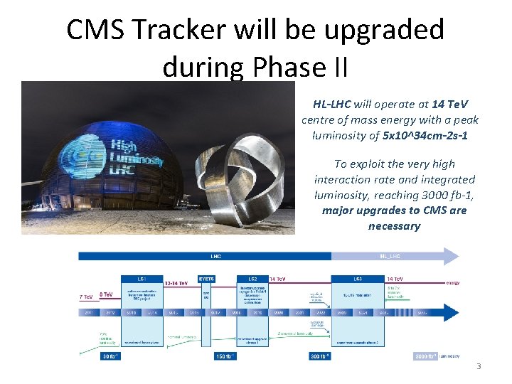
CMS Tracker will be upgraded during Phase II HL-LHC will operate at 14 Te. V centre of mass energy with a peak luminosity of 5 x 10^34 cm-2 s-1 To exploit the very high interaction rate and integrated luminosity, reaching 3000 fb-1, major upgrades to CMS are necessary 3

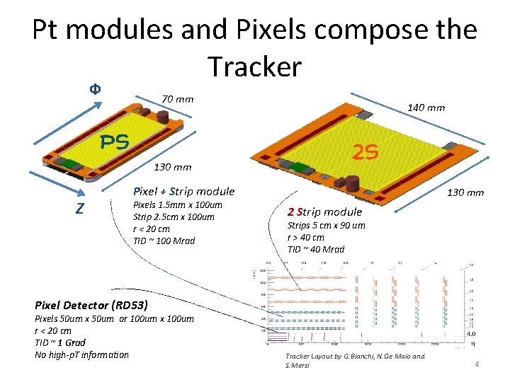
Pt modules and Pixels compose the Tracker Ф 70 mm 140 mm 130 mm Z Pixel + Strip module Pixels 1. 5 mm x 100 um Strip 2. 5 cm x 100 um r < 20 cm TID ~ 100 Mrad 130 mm 2 Strip module Strips 5 cm x 90 um r > 40 cm TID ~ 40 Mrad Pixel Detector (RD 53) Pixels 50 um x 50 um or 100 um x 100 um r < 20 cm TID ~ 1 Grad No high-p. T information Tracker Layout by G. Bianchi, N. De Maio and S. Mersi 4

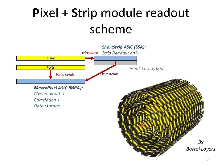
Pixel + Strip module readout scheme wire bonds Short. Strip ASIC (SSA): Strip Readout only STRIP Front-End Hybrid PIXEL bump bonds wire bonds Macro. Pixel ASIC (MPA): Pixel readout + Correlation + Data storage 3 x Barrel Layers 5

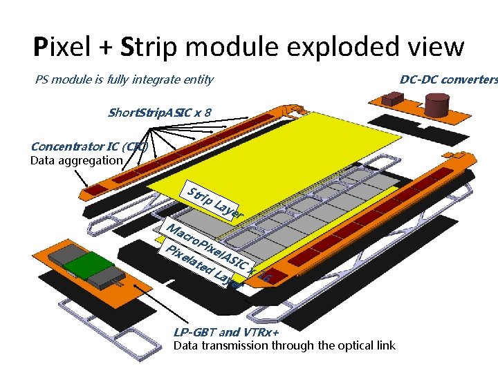
Pixel + Strip module exploded view PS module is fully integrate entity DC-DC converters Short. Strip. ASIC x 8 Concentrator IC (CIC) Data aggregation Str ip r Ma Pix Lay e cro P ela ixe ted l. AS Lay IC er x 1 6 LP-GBT and VTRx+ Data transmission through the optical link 6

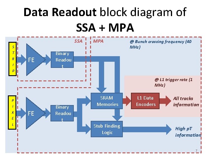
Data Readout block diagram of SSA + MPA SSA S T R I P FE MPA @ Bunch crossing frequency (40 MHz) Binary Readou t @ L 1 trigger rate (1 MHz) P I X E L FE Binary Readou t SRAM Memories Stub Finding Logic L 1 Data Encoders All tracks information High p. T information 7

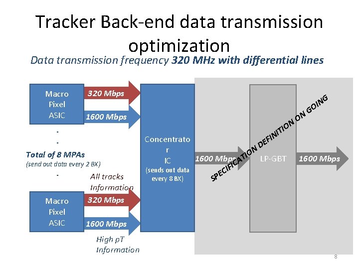
Tracker Back-end data transmission optimization Data transmission frequency 320 MHz with differential lines Macro Pixel ASIC 320 Mbps 1600 Mbps . . Total of 8. MPAs. every 2 BX) (send out data. All tracks Macro Pixel ASIC Information 320 Mbps G O ITI Concentrato FIN E D r N O 1600 Mbps ATI LP-GBT IC IC F I (sends out data EC P every 8 BX) S N ON G N OI 1600 Mbps High p. T Information 8

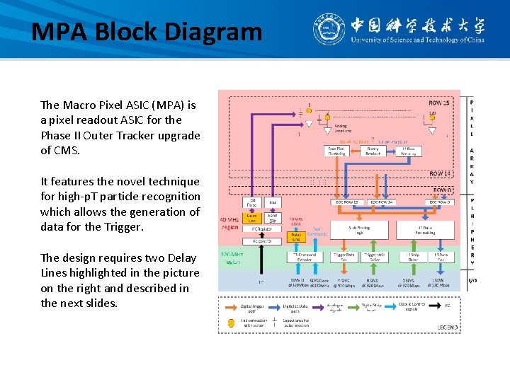
MPA Block Diagram The Macro Pixel ASIC (MPA) is a pixel readout ASIC for the Phase II Outer Tracker upgrade of CMS. It features the novel technique for high-p. T particle recognition which allows the generation of data for the Trigger. The design requires two Delay Lines highlighted in the picture on the right and described in the next slides.

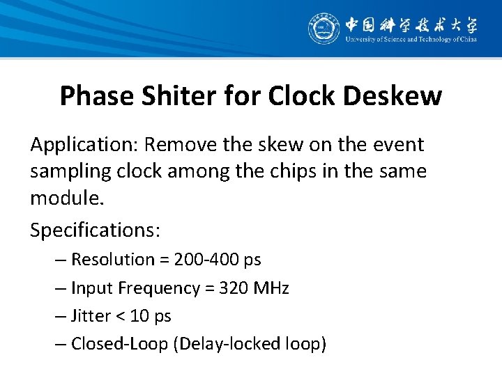
Phase Shiter for Clock Deskew Application: Remove the skew on the event sampling clock among the chips in the same module. Specifications: – Resolution = 200 -400 ps – Input Frequency = 320 MHz – Jitter < 10 ps – Closed-Loop (Delay-locked loop)

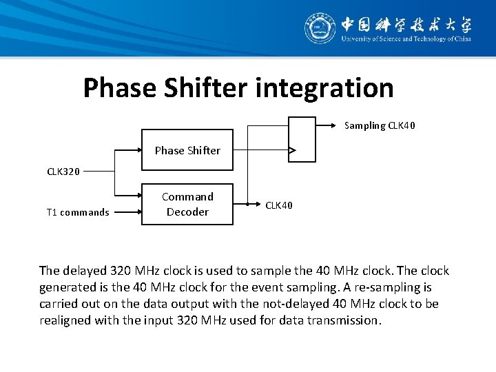
Phase Shifter integration Sampling CLK 40 Phase Shifter CLK 320 T 1 commands Command Decoder CLK 40 The delayed 320 MHz clock is used to sample the 40 MHz clock. The clock generated is the 40 MHz clock for the event sampling. A re-sampling is carried out on the data output with the not-delayed 40 MHz clock to be realigned with the input 320 MHz used for data transmission.

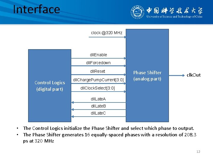
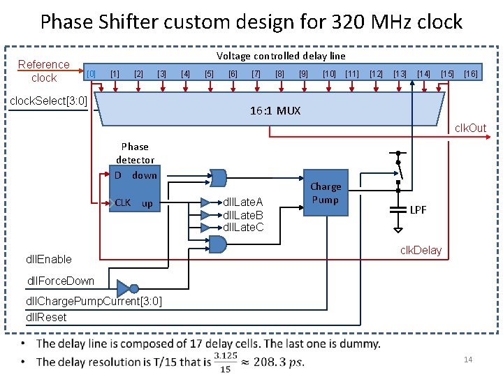
Interface clock @320 MHz dll. Enable dll. Forcedown dll. Reset Control Logics (digital part) dll. Charge. Pump. Current[3: 0] Phase Shifter (analog part) clk. Out dll. Clock. Select[3: 0] dll. Late. A dll. Late. B dll. Late. C • The Control Logics initialize the Phase Shifter and select which phase to output. • The Phase Shifter generates 16 equally-spaced phases with a resolution of 208. 3 ps at 320 MHz 12

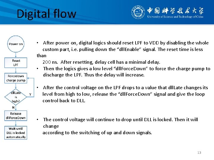
Digital flow • After power on, digital logics should reset LPF to VDD by disabling the whole custom part, i. e. pulling down the “dll. Enable” signal. The reset time is less than 200 ns. After resetting, delay cell has a minimal delay. • Then the logics gives a low level “dll. Force. Down” to force the charge pump to discharge the LPF. Thus the delay will increase. • After the control voltage on the LPF drops to a value that dll. Late changes its level from high to low, release the “dll. Force. Down” signal and give the loop control back to DLL. • The control voltage will continue to drop until DLL is locked. Then it will change according to the switching of up and down signals. 13

Phase Shifter custom design for 320 MHz clock Reference clock Voltage controlled delay line [0] [1] [2] [3] clock. Select[3: 0] [4] [5] [6] [7] [8] [9] [10] [11] [12] [13] [14] [15] [16] 16: 1 MUX clk. Out Phase detector D down CLK up dll. Enable dll. Late. A dll. Late. B dll. Late. C Charge Pump LPF clk. Delay dll. Force. Down dll. Charge. Pump. Current[3: 0] dll. Reset 14

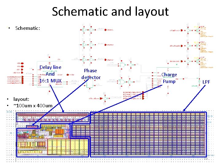
Schematic and layout • Schematic: Delay line And 16: 1 MUX Phase detector Charge Pump LPF • layout: • ~100 um x 400 um 15

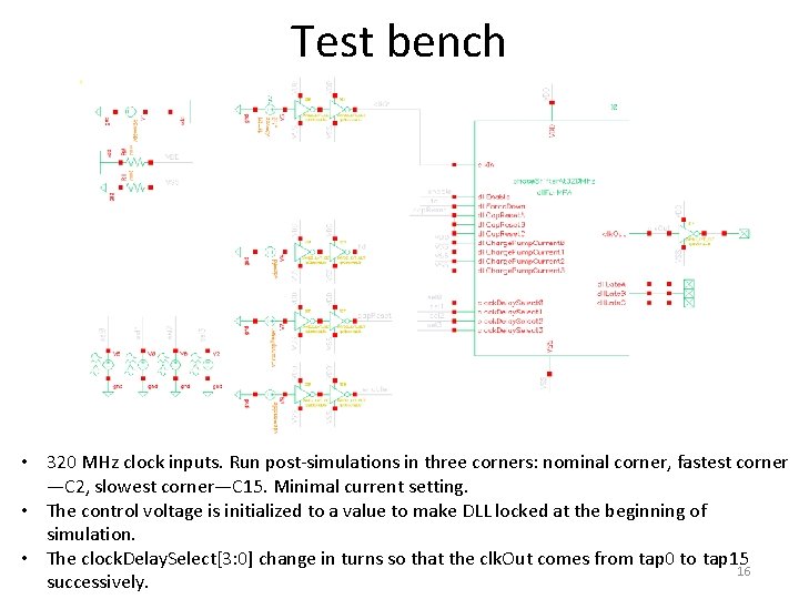
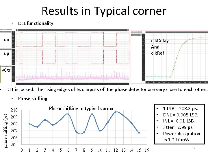
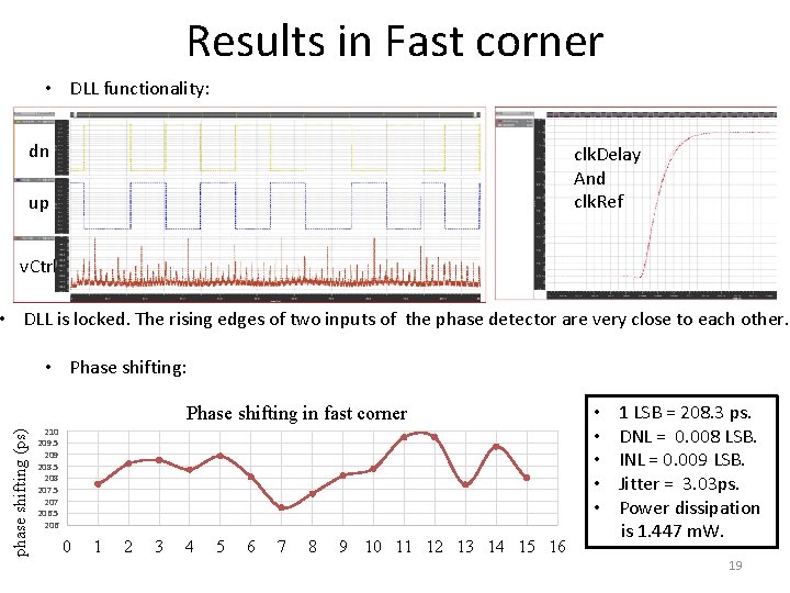
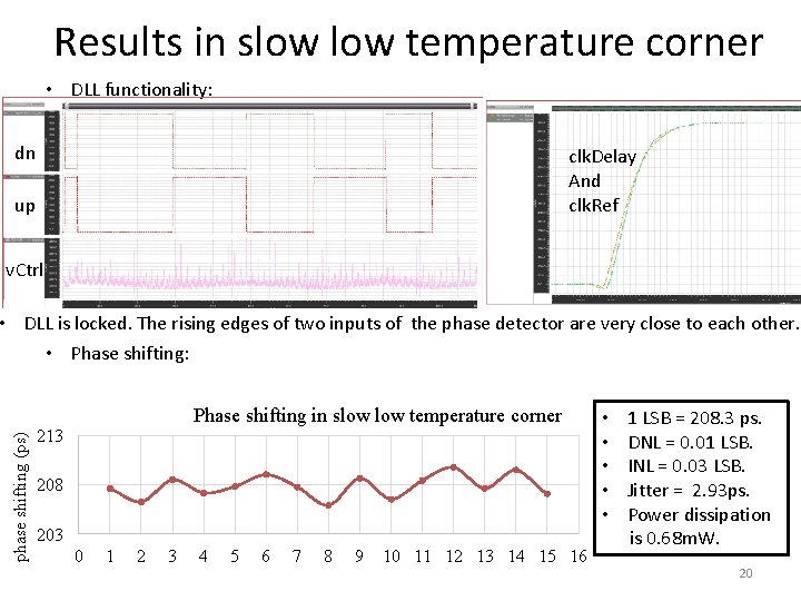
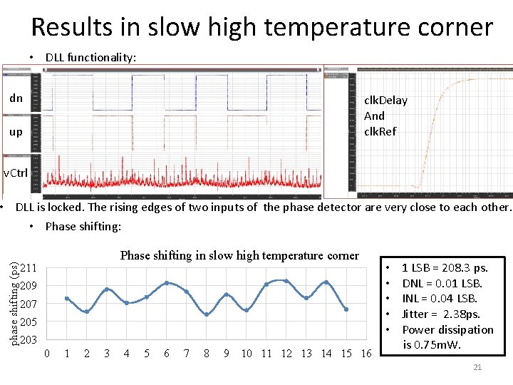
Test bench • 320 MHz clock inputs. Run post-simulations in three corners: nominal corner, fastest corner —C 2, slowest corner—C 15. Minimal current setting. • The control voltage is initialized to a value to make DLL locked at the beginning of simulation. • The clock. Delay. Select[3: 0] change in turns so that the clk. Out comes from tap 0 to tap 15 16 successively.

Corner definition of MPA • • TYPICAL: TT, 1 V, 25 C FAST: FF, 1. 1 V 0 C SLOW TEMPERATURE: SS, 0. 9 V, -40 C SLOW HIGH TEMPERATURE: SS, 0. 9 V, 50 C 17

Results in Typical corner • DLL functionality: dn clk. Delay And clk. Ref up v. Ctrl • DLL is locked. The rising edges of two inputs of the phase detector are very close to each other. phase shifting (ps) • Phase shifting: Phase shifting in typical corner 210 209 208 207 206 205 0 1 2 3 4 5 6 7 8 9 10 11 12 13 14 15 16 • 1 LSB = 208. 3 ps. • DNL = 0. 008 LSB. • INL = 0. 01 LSB. • Jitter =2. 99 ps. • Power dissipation is 1. 007 m. W. 18

Results in Fast corner • DLL functionality: dn clk. Delay And clk. Ref up v. Ctrl • DLL is locked. The rising edges of two inputs of the phase detector are very close to each other. • Phase shifting: phase shifting (ps) Phase shifting in fast corner 210 209. 5 209 208. 5 208 207. 5 207 206. 5 206 0 1 2 3 4 5 6 7 8 9 10 11 12 13 14 15 16 • 1 LSB = 208. 3 ps. • DNL = 0. 008 LSB. • INL = 0. 009 LSB. • Jitter = 3. 03 ps. • Power dissipation is 1. 447 m. W. 19

Results in slow temperature corner • DLL functionality: dn clk. Delay And clk. Ref up v. Ctrl phase shifting (ps) • DLL is locked. The rising edges of two inputs of the phase detector are very close to each other. • Phase shifting: Phase shifting in slow temperature corner 213 208 203 0 1 2 3 4 5 6 7 8 9 10 11 12 13 14 15 16 • 1 LSB = 208. 3 ps. • DNL = 0. 01 LSB. • INL = 0. 03 LSB. • Jitter = 2. 93 ps. • Power dissipation is 0. 68 m. W. 20

Results in slow high temperature corner • DLL functionality: dn clk. Delay And clk. Ref up v. Ctrl phase shifting (ps) • DLL is locked. The rising edges of two inputs of the phase detector are very close to each other. • Phase shifting: Phase shifting in slow high temperature corner 211 209 207 205 203 0 1 2 3 4 5 6 7 8 9 10 11 12 13 14 15 16 • 1 LSB = 208. 3 ps. • DNL = 0. 01 LSB. • INL = 0. 04 LSB. • Jitter = 2. 38 ps. • Power dissipation is 0. 75 m. W. 21

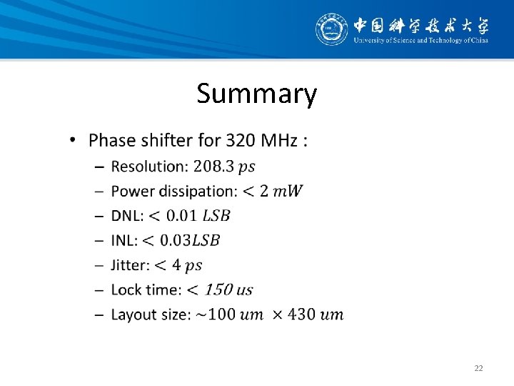
Summary • 22