Multichannel integrated circuits for digital Xray imaging with
![Noise IFED [LSB] IFED SH [LSB] ICAS [LSB] 32 32 32 Temp. versus ICAS Noise IFED [LSB] IFED SH [LSB] ICAS [LSB] 32 32 32 Temp. versus ICAS](https://slidetodoc.com/presentation_image_h/0dcfdfecbe376c0ba9bc58ee2988ea72/image-18.jpg)
![Noise versus IFED [LSB] IFEDSH [LSB] ICAS [LSB] Temp. Gain [ V/el] ( ) Noise versus IFED [LSB] IFEDSH [LSB] ICAS [LSB] Temp. Gain [ V/el] ( )](https://slidetodoc.com/presentation_image_h/0dcfdfecbe376c0ba9bc58ee2988ea72/image-19.jpg)
![Gain, Offset & Noise versus IFEDSH IFED [LSB] IFEDSH [LSB] ICAS [LSB] Temp. Gain Gain, Offset & Noise versus IFEDSH IFED [LSB] IFEDSH [LSB] ICAS [LSB] Temp. Gain](https://slidetodoc.com/presentation_image_h/0dcfdfecbe376c0ba9bc58ee2988ea72/image-21.jpg)
- Slides: 22

Multichannel integrated circuits for digital X-ray imaging with energy windowing Krzysztof Świentek Department of Nuclear Electronics FPNT, AGH Kraków K. Swientek@ftj. agh. edu. pl 2004

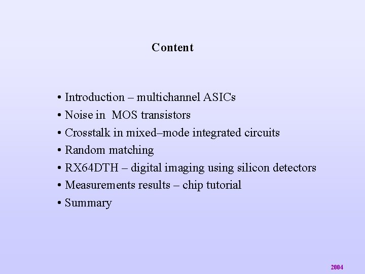
Content • Introduction – multichannel ASICs • Noise in MOS transistors • Crosstalk in mixed–mode integrated circuits • Random matching • RX 64 DTH – digital imaging using silicon detectors • Measurements results – chip tutorial • Summary 2004

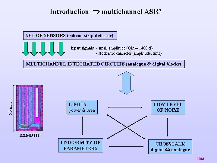
Introduction multichannel ASIC SET OF SENSORS ( silicon strip detector) Input signals - small amplitude (Qin = 1400 el) - stochastic character (amplitude, time) MULTICHANNEL INTEGRATED CIRCUITS (analogue & digital blocks) 6. 5 mm LIMITS: power & area LOW LEVEL OF NOISE RX 64 DTH UNIFORMITY OF PARAMETERS CROSSTALK digital analogue 2004

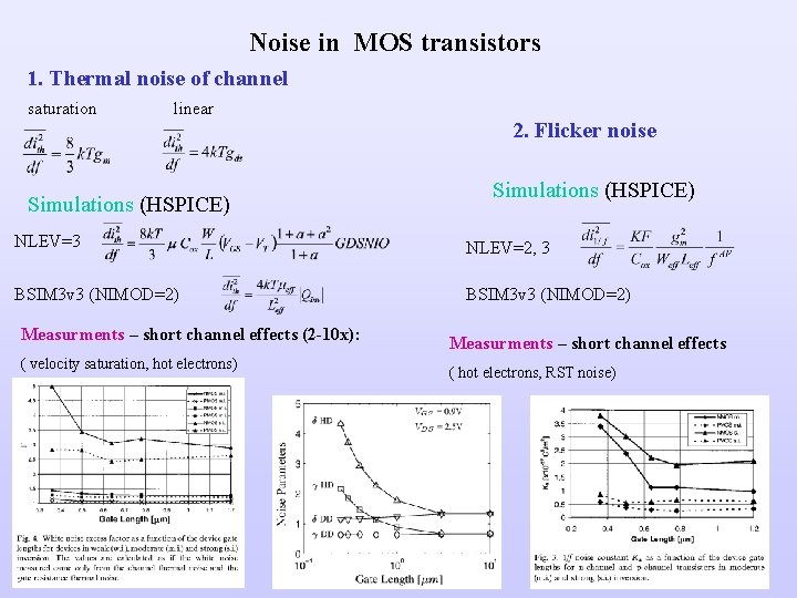
Noise in MOS transistors 1. Thermal noise of channel saturation linear Simulations (HSPICE) 2. Flicker noise Simulations (HSPICE) NLEV=3 NLEV=2, 3 BSIM 3 v 3 (NIMOD=2) Measurments – short channel effects (2 -10 x): ( velocity saturation, hot electrons) Measurments – short channel effects ( hot electrons, RST noise) 2004

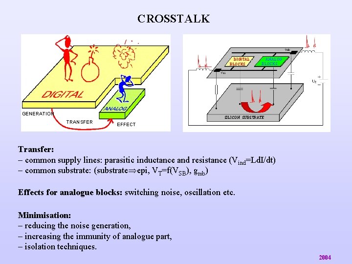
CROSSTALK DIGITAL BLOCKS GENERATION TRANSFER ANALOG BLOCKS SILICON SUBSTRATE EFFECT Transfer: – common supply lines: parasitic inductance and resistance (Vind=Ld. I/dt) – common substrate: (substrate epi, VT=f(VSB), gmb) Effects for analogue blocks: switching noise, oscillation etc. Minimisation: – reducing the noise generation, – increasing the immunity of analogue part, – isolation techniques. 2004

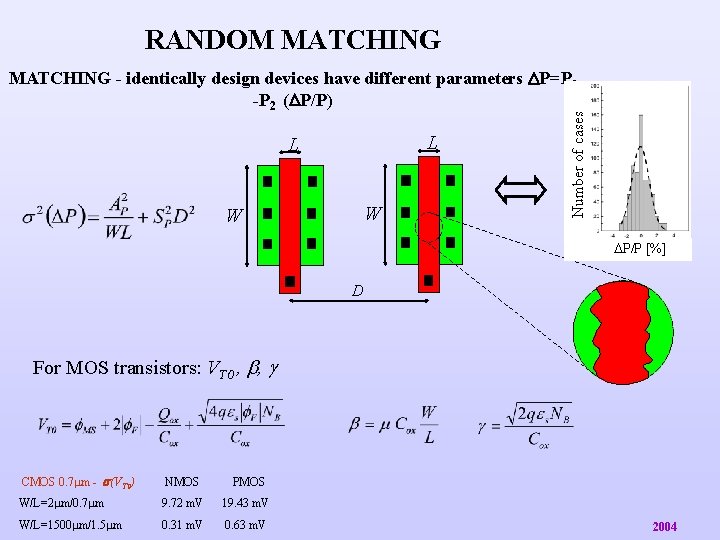
RANDOM MATCHING L L W W Number of cases MATCHING - identically design devices have different parameters P=P 1 -P 2 ( P/P) P/P [%] D For MOS transistors: VT 0 , , CMOS 0. 7 m - (VT 0) NMOS PMOS W/L=2 m/0. 7 m 9. 72 m. V 19. 43 m. V W/L=1500 m/1. 5 m 0. 31 m. V 0. 63 m. V 2004

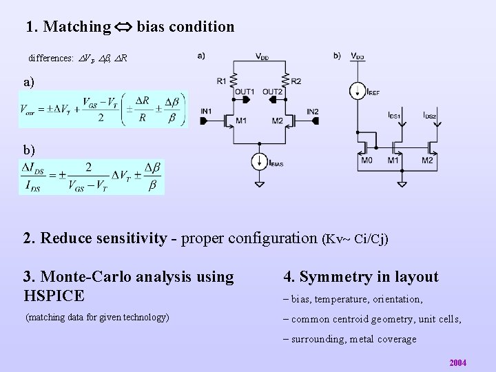
1. Matching bias condition differences: VT, , R a) b) 2. Reduce sensitivity - proper configuration (Kv Ci/Cj) 3. Monte-Carlo analysis using HSPICE 4. Symmetry in layout (matching data for given technology) – common centroid geometry, unit cells, – bias, temperature, orientation, – surrounding, metal coverage 2004

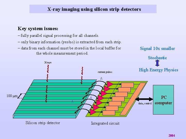
X-ray imaging using silicon strip detectors Key system issues: – fully parallel signal processing for all channels. – only binary information (yes/no) is extracted from each strip. – data from each channel must be stored in the local buffer for the whole measurement period. Signal 10 x smaller Stochastic X-rays current pulses High Energy Physics 100 m data, control Silicon strip detector PC computer Integrated circuit 2004

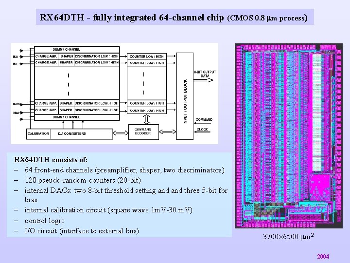
RX 64 DTH - fully integrated 64 -channel chip (CMOS 0. 8 mm process) RX 64 DTH consists of: – 64 front-end channels (preamplifier, shaper, two discriminators) – 128 pseudo-random counters (20 -bit) – internal DACs: two 8 -bit threshold setting and three 5 -bit for bias – internal calibration circuit (square wave 1 m. V-30 m. V) – control logic – I/O circuit (interface to external bus) 3700 6500 m 2 2004

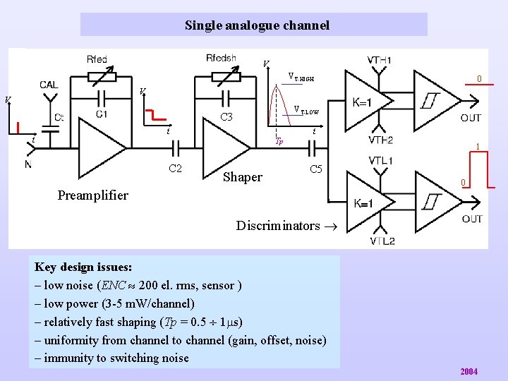
Single analogue channel V VT-HIGH 0 V V VT-LOW C 3 t t t Tp C 2 Shaper 1 C 5 0 Preamplifier Discriminators Key design issues: – low noise (ENC 200 el. rms, sensor ) – low power (3 -5 m. W/channel) – relatively fast shaping (Tp = 0. 5 1 s) – uniformity from channel to channel (gain, offset, noise) – immunity to switching noise 2004

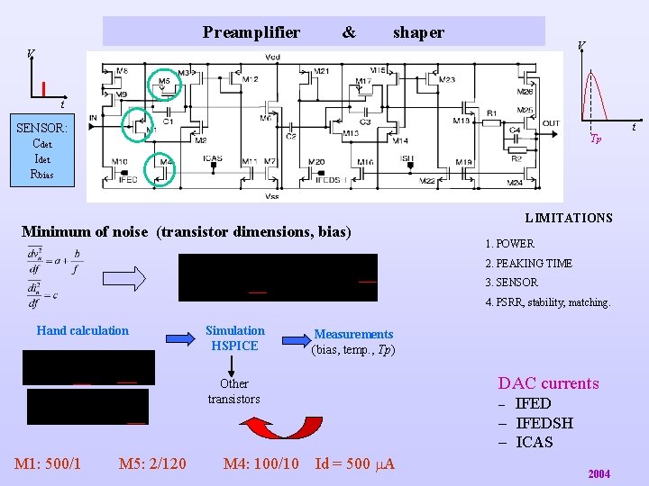
Preamplifier & shaper V V t t SENSOR: Cdet Idet Rbias Tp Minimum of noise (transistor dimensions, bias) LIMITATIONS 1. POWER 2. PEAKING TIME 3. SENSOR 4. PSRR, stability, matching. Hand calculation Simulation HSPICE Measurements (bias, temp. , Tp) DAC currents Other transistors M 1: 500/1 M 5: 2/120 M 4: 100/10 IFED – IFEDSH – ICAS – Id = 500 A 2004

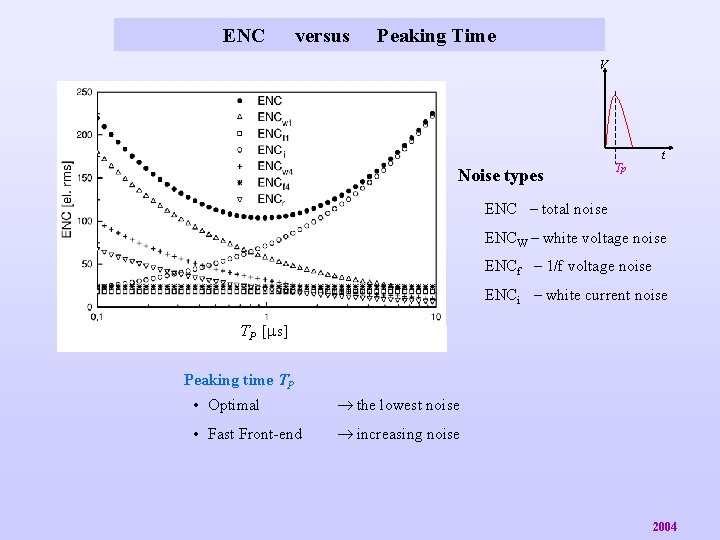
ENC versus Peaking Time V t Noise types Tp ENC – total noise ENCW – white voltage noise ENCf – 1/f voltage noise ENCi – white current noise TP [ s] Peaking time TP • Optimal the lowest noise • Fast Front-end increasing noise 2004

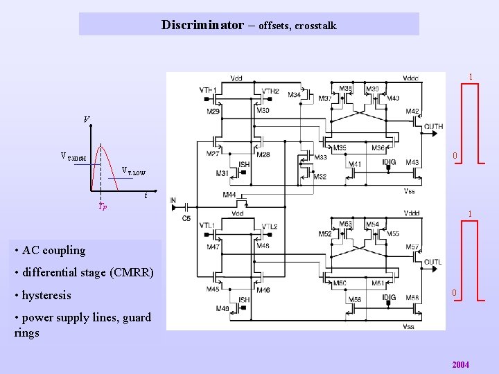
Discriminator – offsets, crosstalk 1 V 0 VT-HIGH VT-LOW t Tp 1 • AC coupling • differential stage (CMRR) • hysteresis 0 • power supply lines, guard rings 2004

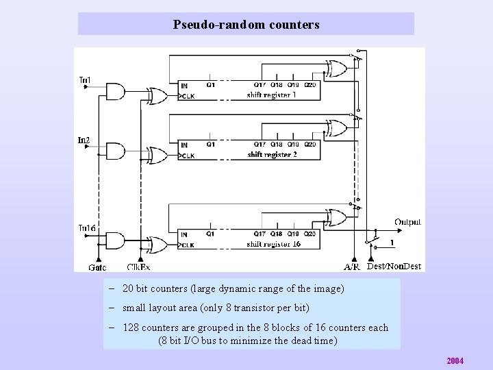
Pseudo-random counters – 20 bit counters (large dynamic range of the image) – small layout area (only 8 transistor per bit) – 128 counters are grouped in the 8 blocks of 16 counters each (8 bit I/O bus to minimize the dead time) 2004

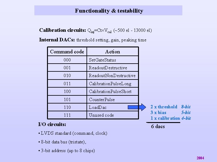
Functionality & testability Calibration circuits: Qinj=Ct Vcal ( 500 el - 13000 el) Internal DACs: threshold setting, gain, peaking time Command code Action 000 Set. Gate. Status 001 Readout. Destructive 010 Readout. Non. Destructive 011 Calibration. Pulse. Long 100 Calibration. Pulse. Short 101 Counter. Pulse 110 Load. Dac 111 Unused code I/O circuits: 2 x threshold 8 -bit 3 x bias 5 -bit 1 x calibration 4 -bit 6 dacs • LVDS standard (command, clock) • 8 -bit data bus (tristate), • 3 -bit address (up to 8 chips) 2004

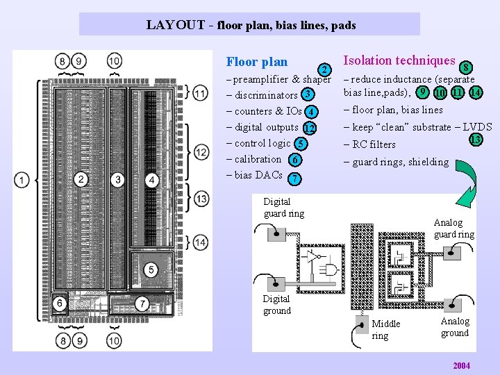
LAYOUT - floor plan, bias lines, pads Floor plan 2 Isolation techniques 8 – preamplifier & shaper – discriminators 3 – reduce inductance (separate bias line, pads), 9 10 11 14 – counters & IOs 4 – digital outputs 12 – control logic 5 – calibration 6 – bias DACs 7 – floor plan, bias lines – keep “clean” substrate – LVDS 13 – RC filters – guard rings, shielding Digital guard ring Analog guard ring Digital ground Middle ring Analog ground 2004

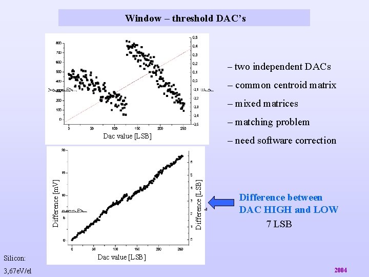
Window – threshold DAC’s – two independent DACs – common centroid matrix – mixed matrices – matching problem Silicon: 3, 67 e. V/el – need software correction Difference [LSB] Difference [m. V] Dac value [LSB] Difference between DAC HIGH and LOW 7 LSB Dac value [LSB] 2004
![Noise IFED LSB IFED SH LSB ICAS LSB 32 32 32 Temp versus ICAS Noise IFED [LSB] IFED SH [LSB] ICAS [LSB] 32 32 32 Temp. versus ICAS](https://slidetodoc.com/presentation_image_h/0dcfdfecbe376c0ba9bc58ee2988ea72/image-18.jpg)
Noise IFED [LSB] IFED SH [LSB] ICAS [LSB] 32 32 32 Temp. versus ICAS & Temp Gain [ V/el] ( ) Offset [m. V] ( ) ENC [el. rms] 8 ke. V ENC [el. rms] 20 ke. V ENC [el. rms] Cal 10 room 57. 63 (0. 34) -9. 23 (1. 91) 248 (6. 1) 232 (7. 7) 232 (24) 32 room 56. 79 (0. 34) -11. 84 (1. 91) 251 (6. 1) 234 (8. 5) 32 40 room 32 32 48 room 32 32 56 room VTH = 255 VTL = scan VTH = scan VTL = 255 219 (24) 56. 30 (0. 37) -11. 50 (1. 96) 233 (7. 5) 217 (7. 3) 213 (15) Source Pu 238 + Cu 203 (13) 32 32 56 25° Vdet = 130 V 191 32 32 63 25° Vdd = 4. 0 V 185 32 32 63 20° Vddd = 4. 0 V 175 32 32 63 18° Peltier element for temp. 163 Controled Temp. 2004
![Noise versus IFED LSB IFEDSH LSB ICAS LSB Temp Gain Vel Noise versus IFED [LSB] IFEDSH [LSB] ICAS [LSB] Temp. Gain [ V/el] ( )](https://slidetodoc.com/presentation_image_h/0dcfdfecbe376c0ba9bc58ee2988ea72/image-19.jpg)
Noise versus IFED [LSB] IFEDSH [LSB] ICAS [LSB] Temp. Gain [ V/el] ( ) Offset [m. V] ( ) ENC [el. rms] 8 ke. V ENC [el. rms] 20 ke. V 24 32 63 20° 54. 86 (0. 39) -17. 62 (1. 33) 198. 9 (5. 1) 205. 9 (16. 7) 32 32 63 20° 54. 85 (0. 44) -17. 85 (1. 09) 203. 1 (6. 6) 201. 5 (8. 22) 40 32 63 20° 54. 86 (0. 45) -17. 55 (1. 26) 220. 7 (8. 5) 213. 7 (9. 47) 48 32 63 20° 54. 84 (0. 49) -16. 96 (1. 30) 238. 2 (9. 2) 228. 6 (9. 46) – gain & offset const – window is 5 LSB – Peltier element } fast noise increasing pin-holes in detector leakeage current dead channels because out of operating point increase IFED but. . . rescue 2004

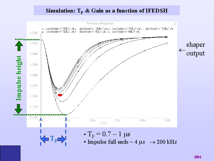
Simulation: TP & Gain as a function of IFEDSH Impulse height shaper output TP • TP = 0. 7 – 1 s • Impulse fall ends 4 s 200 k. Hz 2004
![Gain Offset Noise versus IFEDSH IFED LSB IFEDSH LSB ICAS LSB Temp Gain Gain, Offset & Noise versus IFEDSH IFED [LSB] IFEDSH [LSB] ICAS [LSB] Temp. Gain](https://slidetodoc.com/presentation_image_h/0dcfdfecbe376c0ba9bc58ee2988ea72/image-21.jpg)
Gain, Offset & Noise versus IFEDSH IFED [LSB] IFEDSH [LSB] ICAS [LSB] Temp. Gain [ V/el] ( ) Offset [m. V] ( ) ENC [el. rms] 20 ke. V 32 16 63 20° 80. 54 (0. 57) -0. 8 (0. 9) 177. 5 (4. 91) 32 24 63 20° 63. 74 (0. 52) -11. 68 (1. 11) 197. 6 (8. 69) 54. 85 (0. 44) -17. 85 (1. 09) 201. 5 (8. 22) 32 32 63 20° 32 40 63 20° 50. 2 (0. 36) -20. 59 (1. 24) 206. 5 (9. 42) 32 48 63 20° 47. 64 (0. 35) -21. 67 (1. 39) 209. 9 (8. 92) 32 63 63 20° 45. 52 (0. 32) -22. 82 (1. 22) 210. 7 (9. 36) – window is 5 LSB – Peltier element max (slow) peaking time TP min (fast) 2004

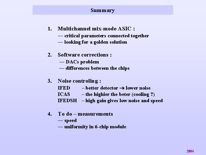
Summary 1. Multichannel mix-mode ASIC : — critical parameters connected together — looking for a golden solution 2. Software corrections : — DACs problem — differences between the chips 3. Noise controling : IFED – better detector lower noise ICAS – the highier the beter (cooling ? ) IFEDSH – high gain gives low noise and speed 4. To do – measurements — speed — uniformity in 6 -chip module 2004