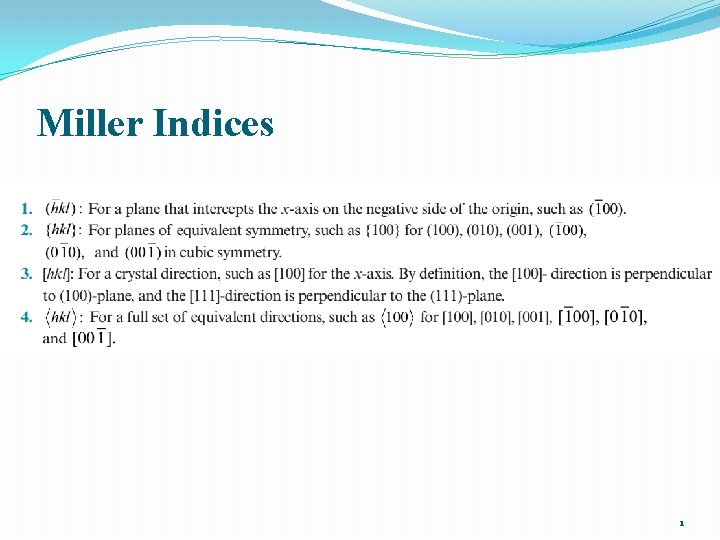
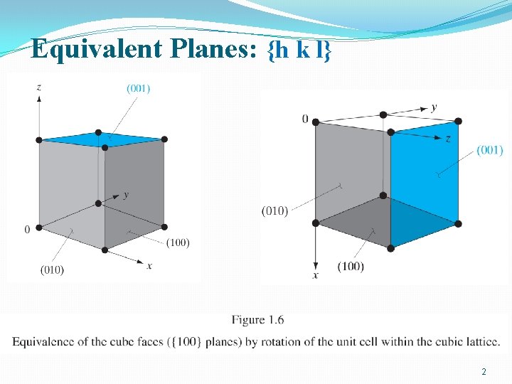
Miller Indices 1 Equivalent Planes h k l
![Crystal Directions: [h k l] 3 Crystal Directions: [h k l] 3](https://slidetodoc.com/presentation_image_h2/94cc0c572c292a84b8b7866ce8b9efb2/image-3.jpg)

- Slides: 73

Miller Indices 1

Equivalent Planes: {h k l} 2
![Crystal Directions h k l 3 Crystal Directions: [h k l] 3](https://slidetodoc.com/presentation_image_h2/94cc0c572c292a84b8b7866ce8b9efb2/image-3.jpg)
Crystal Directions: [h k l] 3

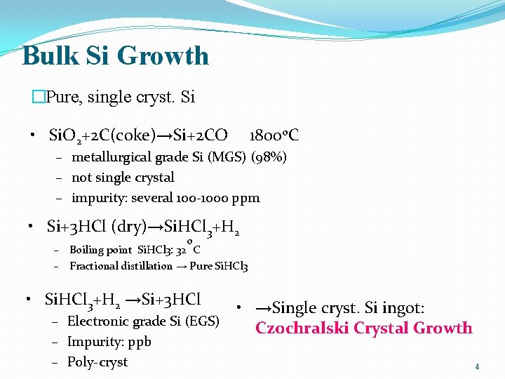
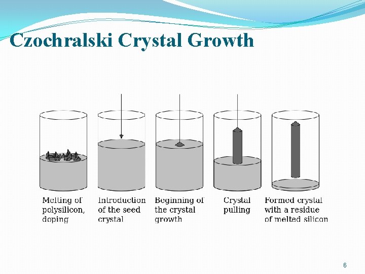
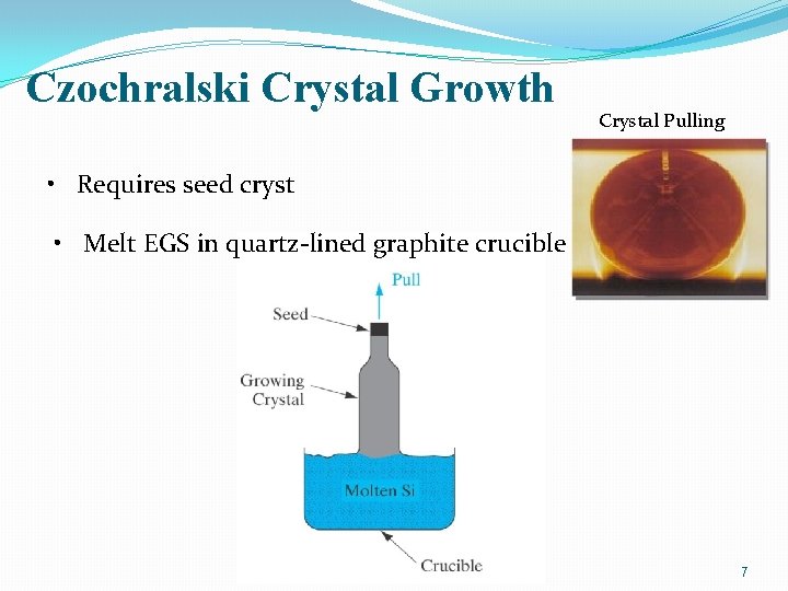
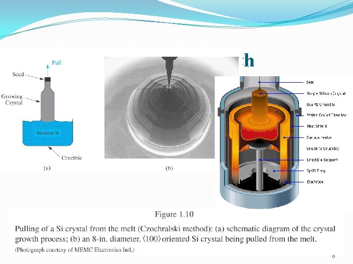
Bulk Si Growth �Pure, single cryst. Si • Si. O 2+2 C(coke)→Si+2 CO 1800 o. C – metallurgical grade Si (MGS) (98%) – not single crystal – impurity: several 100 -1000 ppm • Si+3 HCl (dry)→Si. HCl 3+H 2 o – Boiling point Si. HCl 3: 32 C – Fractional distillation → Pure Si. HCl 3 • Si. HCl 3+H 2 →Si+3 HCl • →Single cryst. Si ingot: – Electronic grade Si (EGS) Czochralski Crystal Growth – Impurity: ppb – Poly-cryst 4

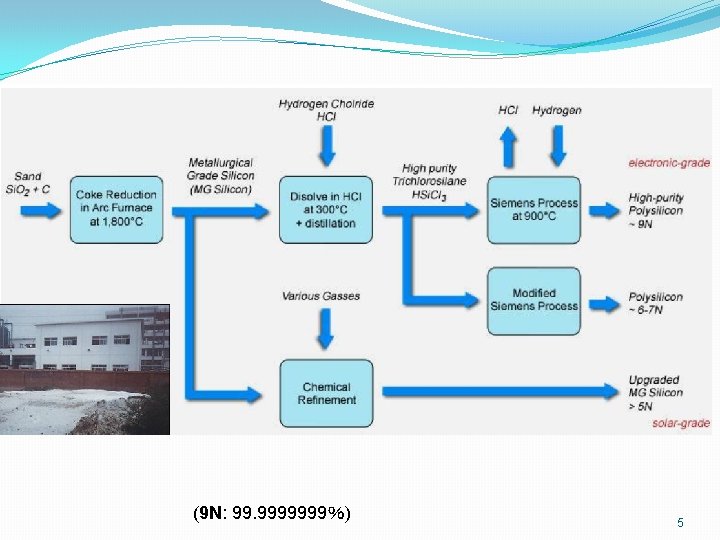
From Sand to Silicon (9 N: 99. 9999999%) 5

Czochralski Crystal Growth 6

Czochralski Crystal Growth Crystal Pulling • Requires seed cryst • Melt EGS in quartz-lined graphite crucible 7

Czochralski Crystal Growth 8

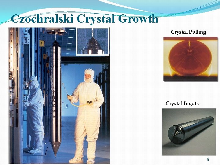
Czochralski Crystal Growth Crystal Pulling Crystal Ingots 9

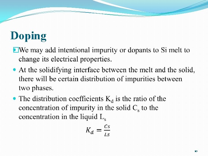
Doping � 10

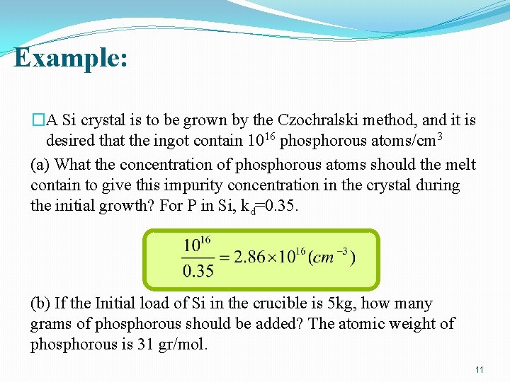
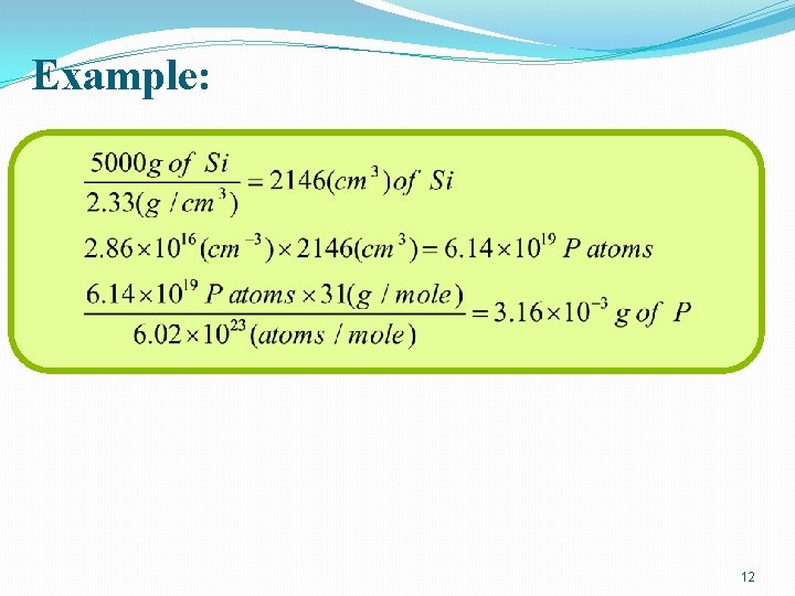
Example: �A Si crystal is to be grown by the Czochralski method, and it is desired that the ingot contain 1016 phosphorous atoms/cm 3 (a) What the concentration of phosphorous atoms should the melt contain to give this impurity concentration in the crystal during the initial growth? For P in Si, kd=0. 35. (b) If the Initial load of Si in the crucible is 5 kg, how many grams of phosphorous should be added? The atomic weight of phosphorous is 31 gr/mol. 11

Example: 12

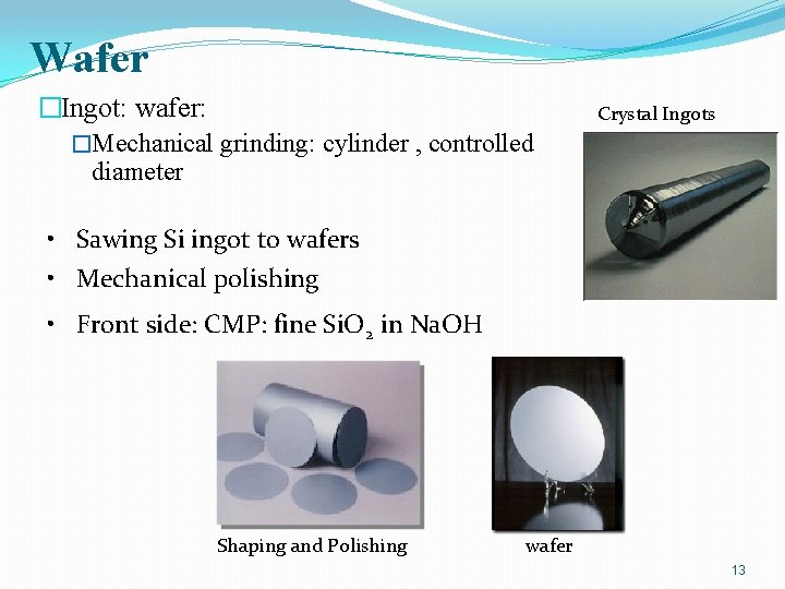
Wafer �Ingot: wafer: �Mechanical grinding: cylinder , controlled diameter Crystal Ingots • Sawing Si ingot to wafers • Mechanical polishing • Front side: CMP: fine Si. O 2 in Na. OH Shaping and Polishing wafer 13

Wafer �Ingot: wafer: �Mechanical grinding: cylinder , controlled diameter Crystal Ingots • Sawing Si ingot to wafers • Mechanical polishing • Front side: CMP: fine Si. O 2 in Na. OH Shaping and Polishing wafer 14

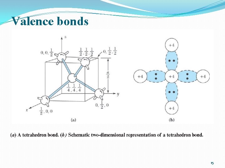
Valence bonds 15

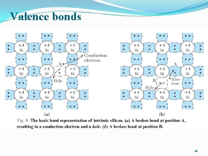
Valence bonds 16

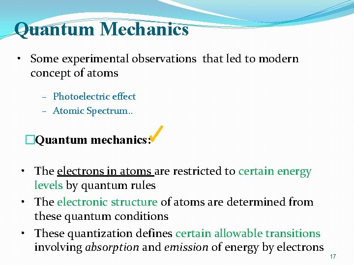
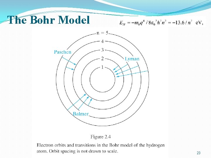
Quantum Mechanics • Some experimental observations that led to modern concept of atoms – Photoelectric effect – Atomic Spectrum. . �Quantum mechanics: • The electrons in atoms are restricted to certain energy levels by quantum rules • The electronic structure of atoms are determined from these quantum conditions • These quantization defines certain allowable transitions involving absorption and emission of energy by electrons 17

Quantum Mechanics �In 1920 it becomes necessary to develop a new theory to describe phenomena on the atomic scale �Many events involving electrons and atoms did not obey the classical laws of mechanics �A new kind of mechanics to describe the behavior of particles on the small scale : Quantum mechanics: Ø Describes atomic phenomena very well Ø Predicts the way in which electrons behave in solids 18

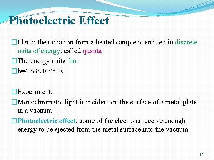
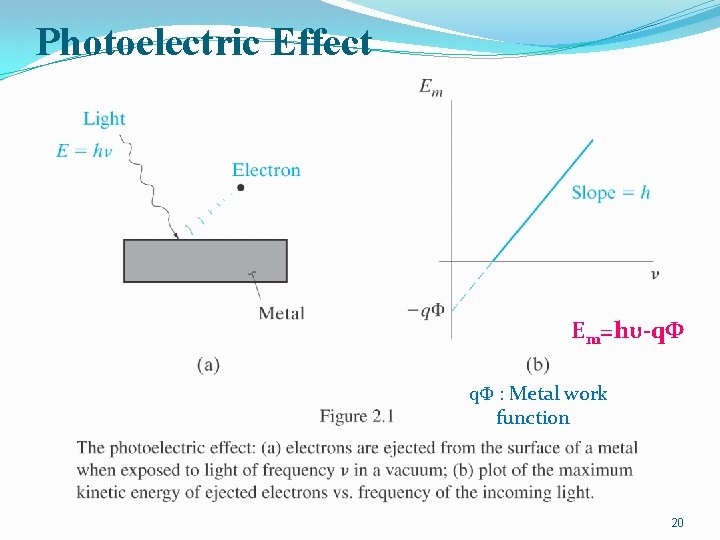
Photoelectric Effect �Plank: the radiation from a heated sample is emitted in discrete units of energy, called quanta �The energy units: hυ �h=6. 63× 10 -34 J. s �Experiment: �Monochromatic light is incident on the surface of a metal plate in a vacuum �Photoelectric effect: some of the electrons receive enough energy to be ejected from the metal surface into the vacuum 19

Photoelectric Effect Em=hυ-qΦ qΦ : Metal work function 20

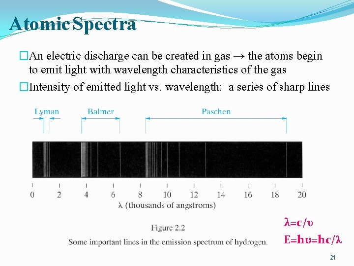
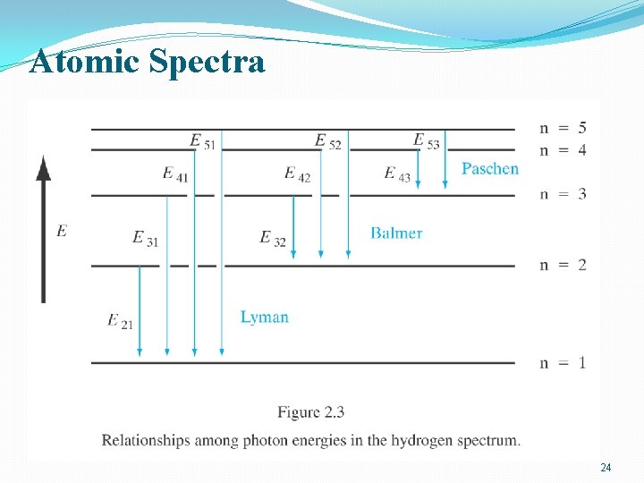
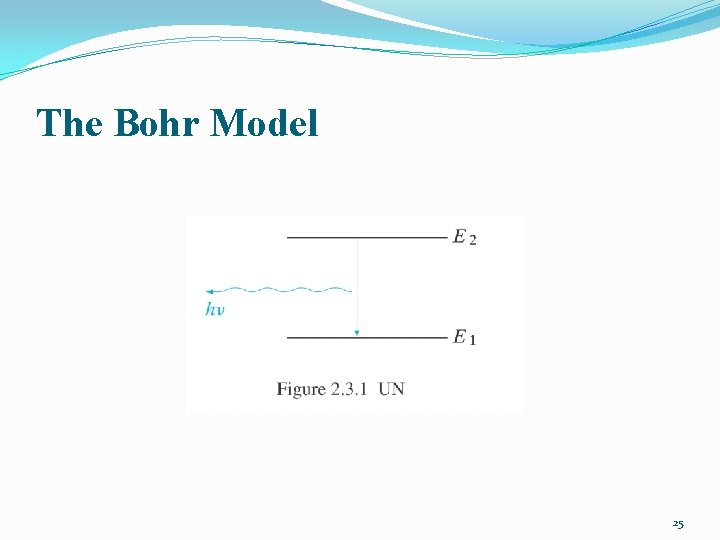
Atomic Spectra �An electric discharge can be created in gas → the atoms begin to emit light with wavelength characteristics of the gas �Intensity of emitted light vs. wavelength: a series of sharp lines λ=c/υ E=hυ=hc/λ 21

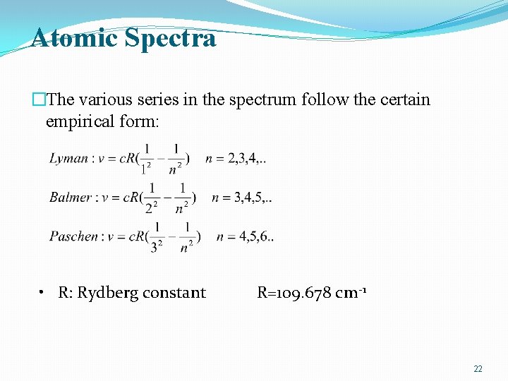
Atomic Spectra �The various series in the spectrum follow the certain empirical form: • R: Rydberg constant R=109. 678 cm-1 22

The Bohr Model 23

Atomic Spectra 24

The Bohr Model 25

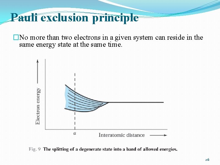
Pauli exclusion principle �No more than two electrons in a given system can reside in the same energy state at the same time. 26

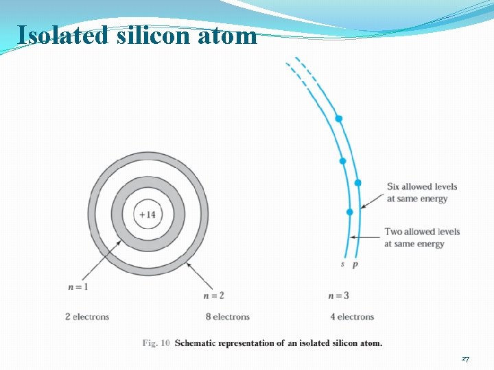
Isolated silicon atom 27

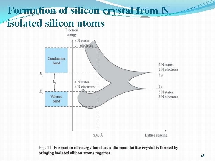
Formation of silicon crystal from N isolated silicon atoms 28

Energy Bands �At 0 K the electrons will occupy the lowest energy states available to them �For Si crystal: 4 N states in the valence band available to the 4 N electrons �→ at 0 K: every states in the valence band is filled /conduction band: empty 29

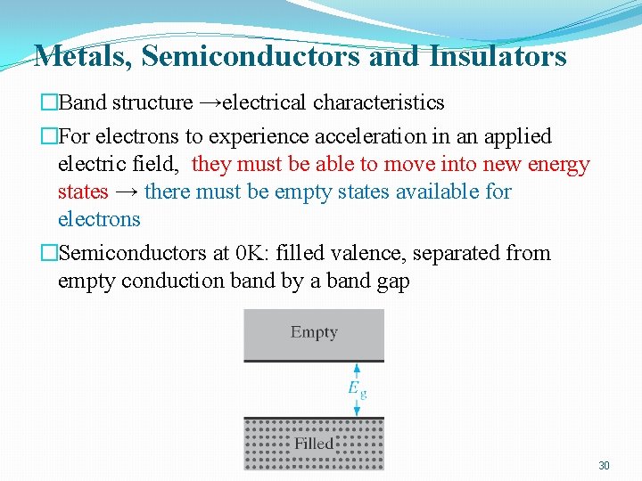
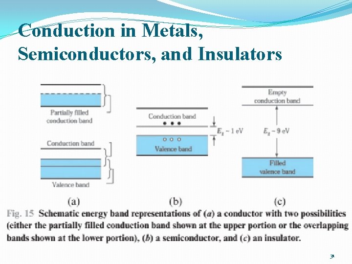
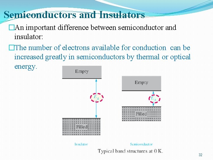
Metals, Semiconductors and Insulators �Band structure →electrical characteristics �For electrons to experience acceleration in an applied electric field, they must be able to move into new energy states → there must be empty states available for electrons �Semiconductors at 0 K: filled valence, separated from empty conduction band by a band gap 30

Conduction in Metals, Semiconductors, and Insulators 31

Semiconductors and Insulators �An important difference between semiconductor and insulator: �The number of electrons available for conduction can be increased greatly in semiconductors by thermal or optical energy. 32

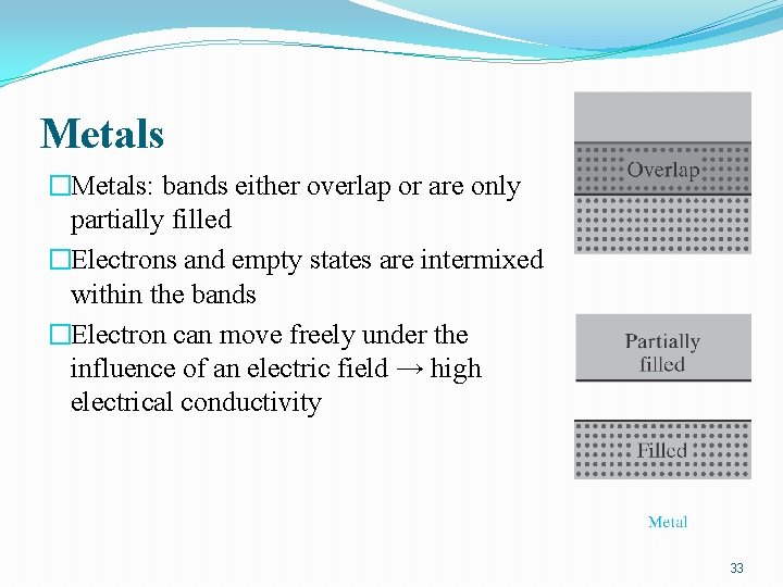
Metals �Metals: bands either overlap or are only partially filled �Electrons and empty states are intermixed within the bands �Electron can move freely under the influence of an electric field → high electrical conductivity 33

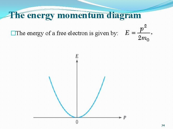
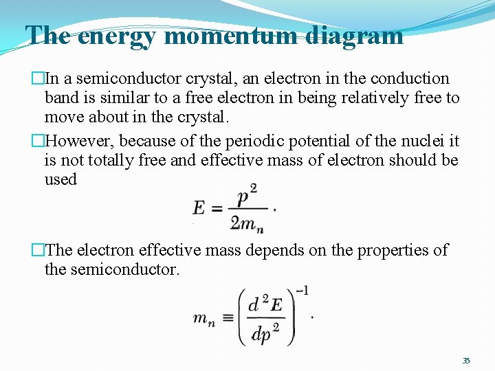
The energy momentum diagram �The energy of a free electron is given by: 34

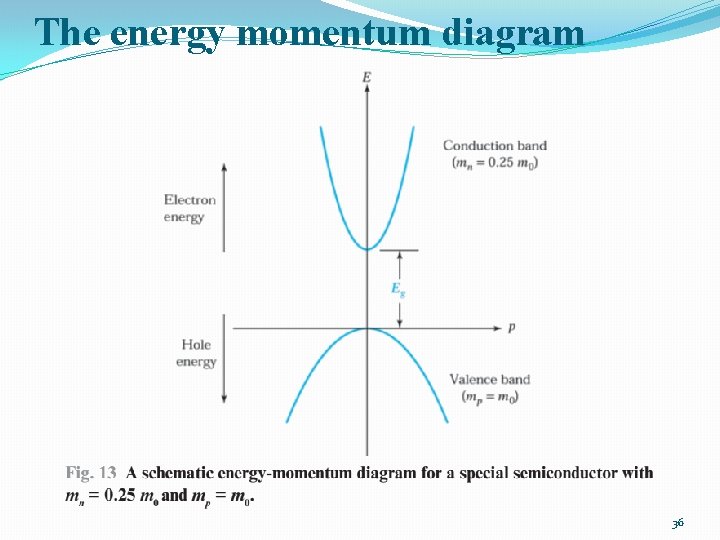
The energy momentum diagram �In a semiconductor crystal, an electron in the conduction band is similar to a free electron in being relatively free to move about in the crystal. �However, because of the periodic potential of the nuclei it is not totally free and effective mass of electron should be used �The electron effective mass depends on the properties of the semiconductor. 35

The energy momentum diagram 36

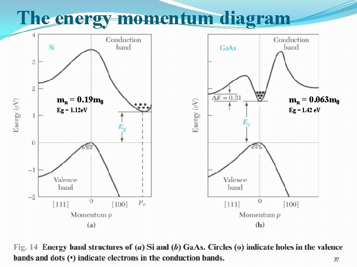
The energy momentum diagram mn = 0. 19 m 0 mn = 0. 063 m 0 Eg = 1. 12 e. V Eg = 1. 42 e. V 37

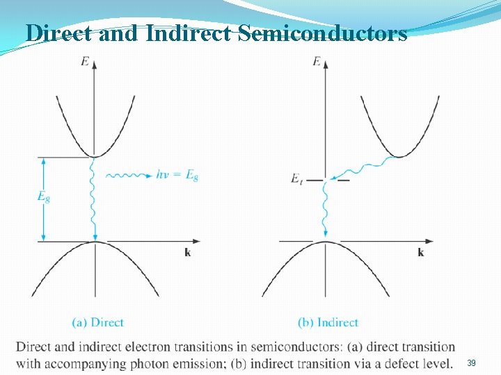
Direct and indirect semiconductors �Direct semiconductor does not require a change in momentum for an electron transition from the valence band to the conduction band. (Ga. As) �Indirect semiconductor a change of momentum is required in a transition. �Light-emitting diodes and semiconductor lasers use direct semiconductors. 38

Direct and Indirect Semiconductors 39

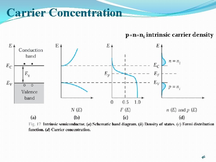
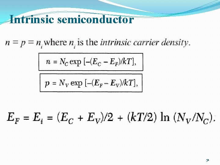
INTRINSIC CARRIER CONCENTRATION �Thermal equilibrium: The steady-state condition at a given temperature without any external excitations such as light, pressure, or an electric field. �Intrinsic semiconductor: Contains relatively small amounts of impurities compared with thermally generated electrons and holes. (a perfect semiconductor crystal with no impurities or lattice defects) �EHPs are the only charge carriers in intrinsic material �n=p=ni 40

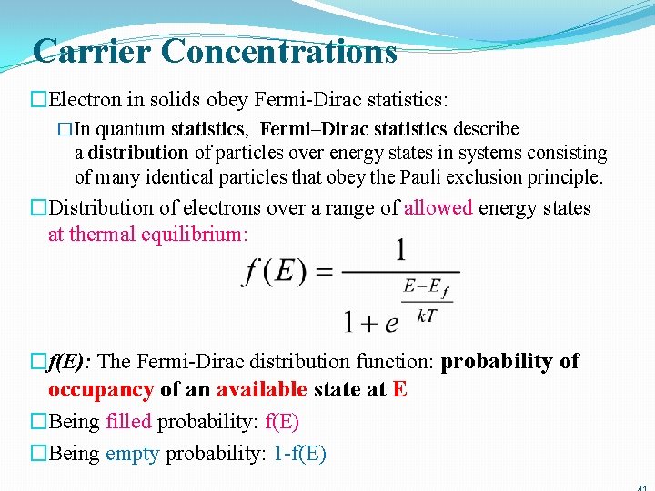
Carrier Concentrations �Electron in solids obey Fermi-Dirac statistics: �In quantum statistics, Fermi–Dirac statistics describe a distribution of particles over energy states in systems consisting of many identical particles that obey the Pauli exclusion principle. �Distribution of electrons over a range of allowed energy states at thermal equilibrium: �f(E): The Fermi-Dirac distribution function: probability of occupancy of an available state at E �Being filled probability: f(E) �Being empty probability: 1 -f(E)

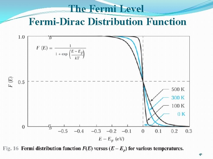
The Fermi Level Fermi-Dirac Distribution Function 42

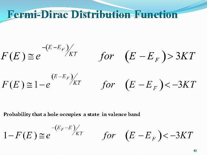
Fermi-Dirac Distribution Function Probability that a hole occupies a state in valence band 43

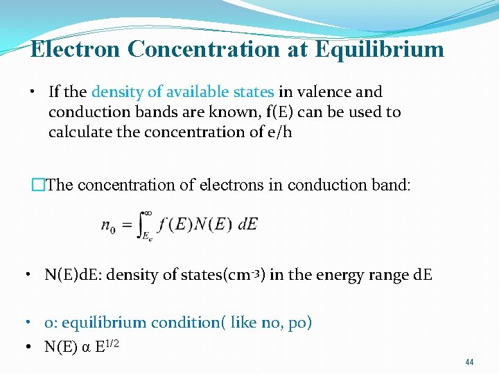
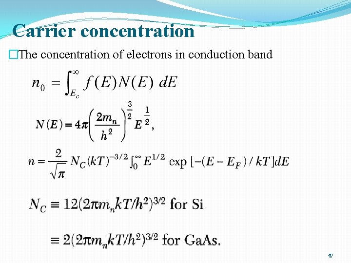
Electron Concentration at Equilibrium • If the density of available states in valence and conduction bands are known, f(E) can be used to calculate the concentration of e/h �The concentration of electrons in conduction band: • N(E)d. E: density of states(cm-3) in the energy range d. E • 0: equilibrium condition( like n 0, p 0) • N(E) α E 1/2 44

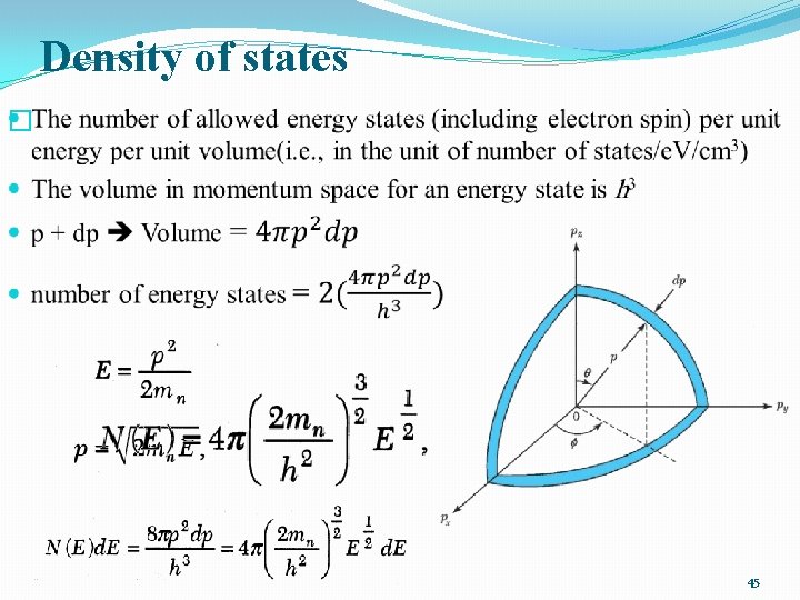
Density of states � 45

Carrier Concentration p=n=ni intrinsic carrier density 46

Carrier concentration �The concentration of electrons in conduction band 47

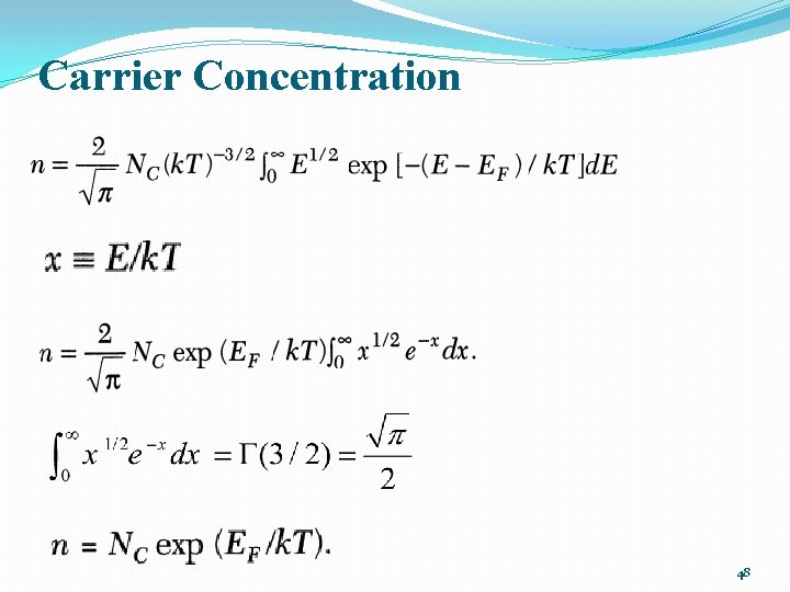
Carrier Concentration 48

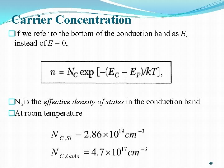
Carrier Concentration �If we refer to the bottom of the conduction band as Ec instead of E = 0, �Nc is the effective density of states in the conduction band �At room temperature 49

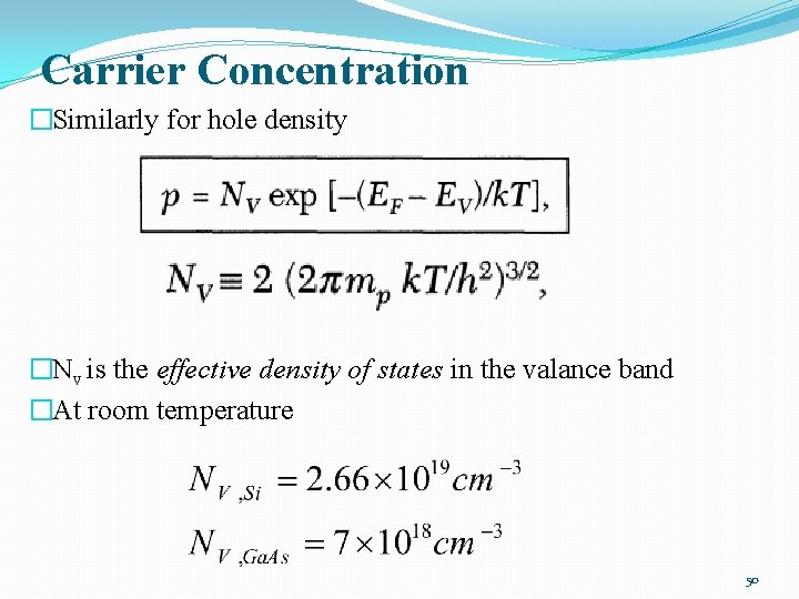
Carrier Concentration �Similarly for hole density �Nv is the effective density of states in the valance band �At room temperature 50

Intrinsic semiconductor 51

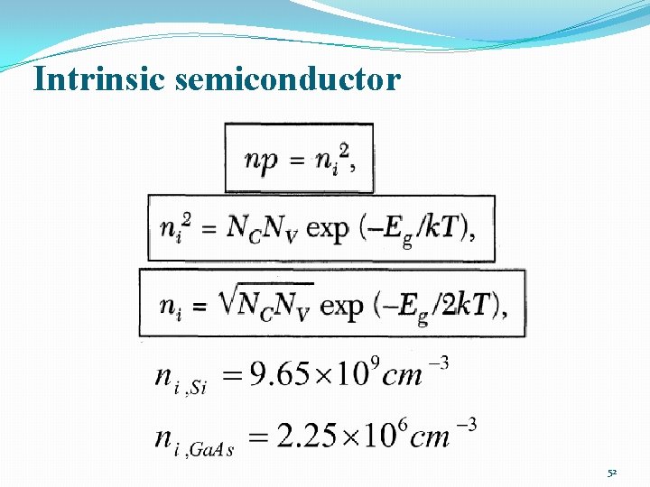
Intrinsic semiconductor 52

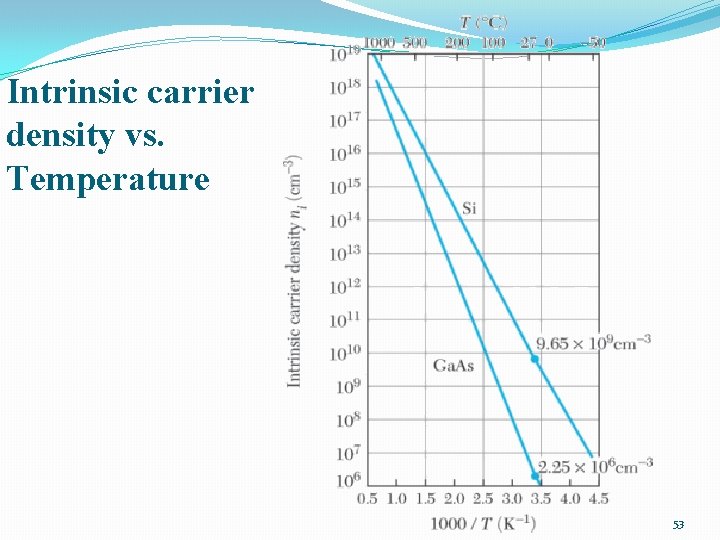
Intrinsic carrier density vs. Temperature 53

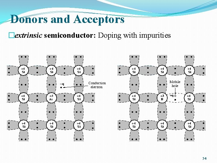
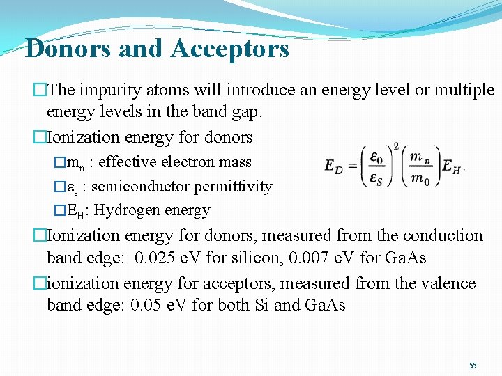
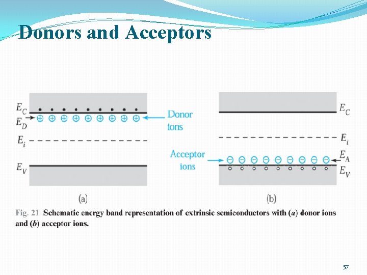
Donors and Acceptors �extrinsic semiconductor: Doping with impurities 54

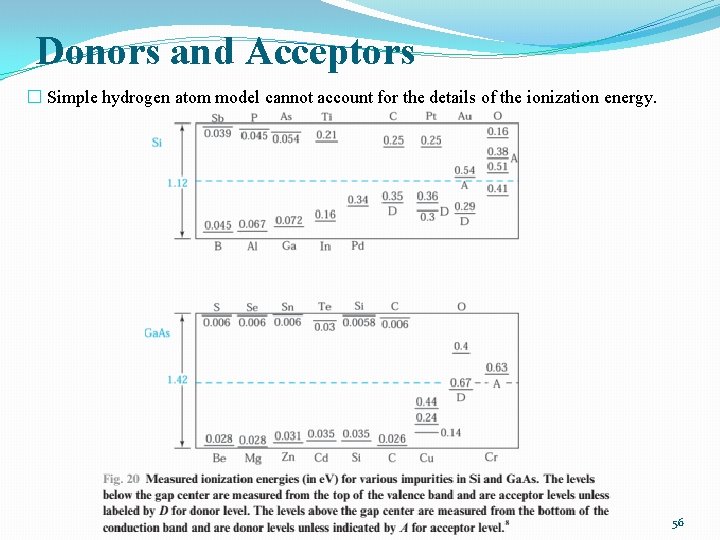
Donors and Acceptors �The impurity atoms will introduce an energy level or multiple energy levels in the band gap. �Ionization energy for donors �mn : effective electron mass � s : semiconductor permittivity �EH: Hydrogen energy �Ionization energy for donors, measured from the conduction band edge: 0. 025 e. V for silicon, 0. 007 e. V for Ga. As �ionization energy for acceptors, measured from the valence band edge: 0. 05 e. V for both Si and Ga. As 55

Donors and Acceptors � Simple hydrogen atom model cannot account for the details of the ionization energy. 56

Donors and Acceptors 57

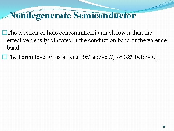
Nondegenerate Semiconductor �The electron or hole concentration is much lower than the effective density of states in the conduction band or the valence band. �The Fermi level EF is at least 3 k. T above EV or 3 k. T below EC. 58

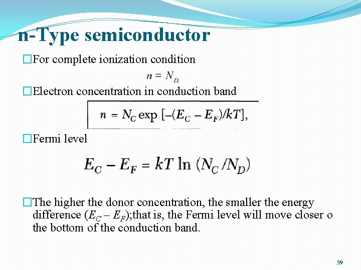
n-Type semiconductor �For complete ionization condition �Electron concentration in conduction band �Fermi level �The higher the donor concentration, the smaller the energy difference (EC – EF); that is, the Fermi level will move closer o the bottom of the conduction band. 59

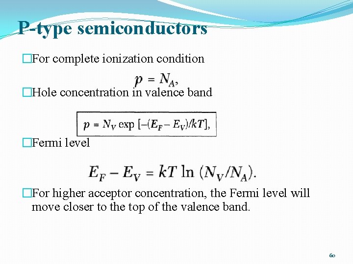
P-type semiconductors �For complete ionization condition �Hole concentration in valence band �Fermi level �For higher acceptor concentration, the Fermi level will move closer to the top of the valence band. 60

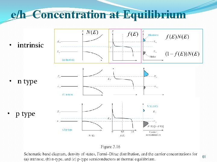
e/h Concentration at Equilibrium • intrinsic • n type • p type 61

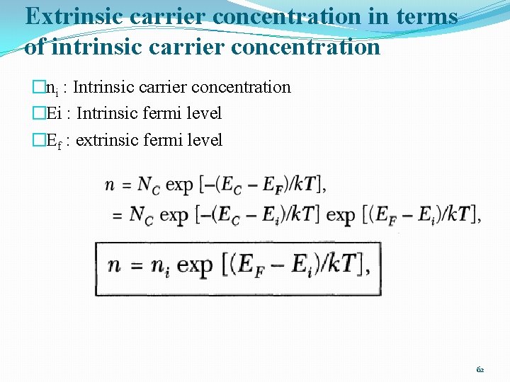
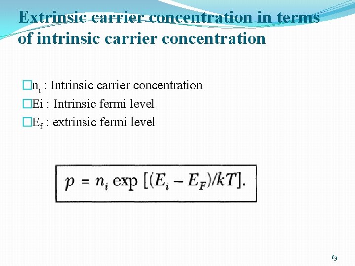
Extrinsic carrier concentration in terms of intrinsic carrier concentration �ni : Intrinsic carrier concentration �Ei : Intrinsic fermi level �Ef : extrinsic fermi level 62

Extrinsic carrier concentration in terms of intrinsic carrier concentration �ni : Intrinsic carrier concentration �Ei : Intrinsic fermi level �Ef : extrinsic fermi level 63

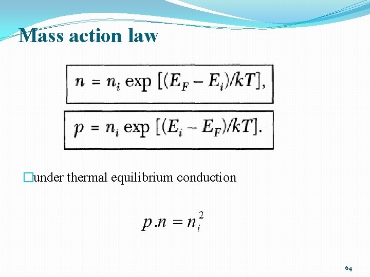
Mass action law �under thermal equilibrium conduction 64

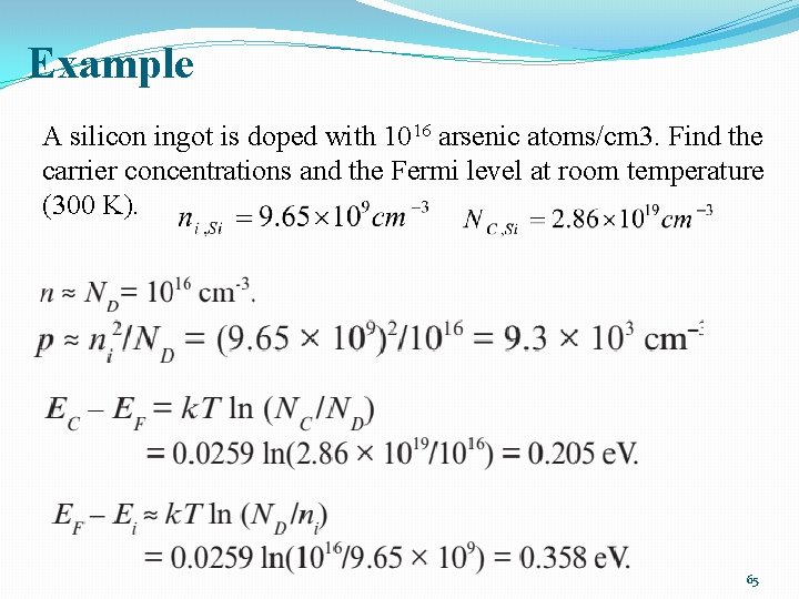
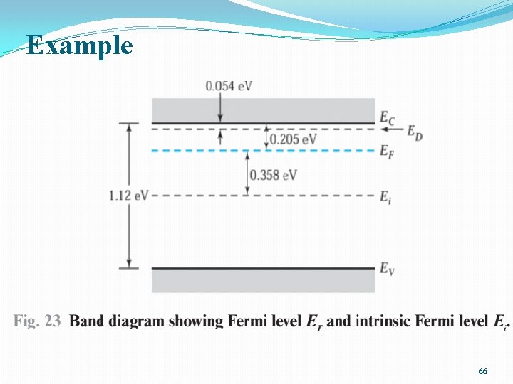
Example A silicon ingot is doped with 1016 arsenic atoms/cm 3. Find the carrier concentrations and the Fermi level at room temperature (300 K). 65

Example 66

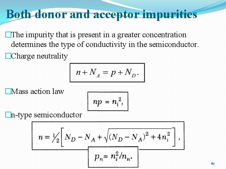
Both donor and acceptor impurities �The impurity that is present in a greater concentration determines the type of conductivity in the semiconductor. �Charge neutrality �Mass action law �n-type semiconductor 67

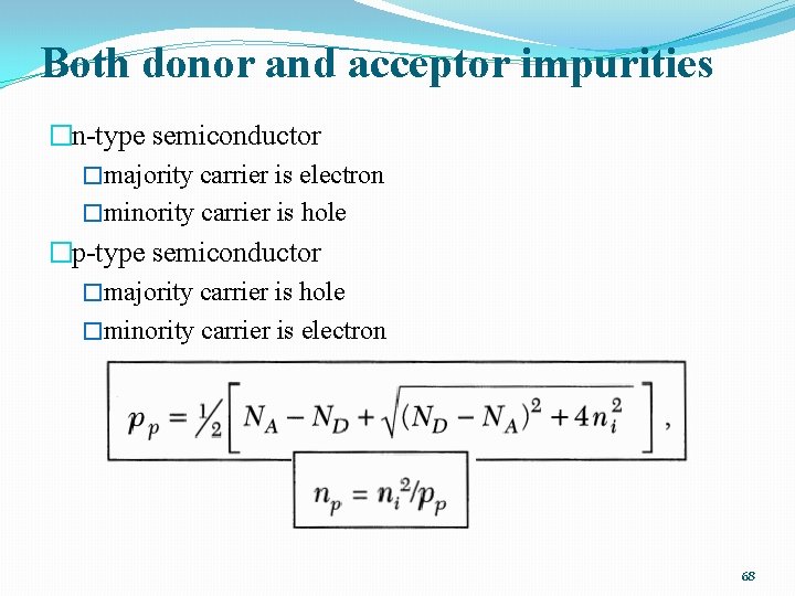
Both donor and acceptor impurities �n-type semiconductor �majority carrier is electron �minority carrier is hole �p-type semiconductor �majority carrier is hole �minority carrier is electron 68

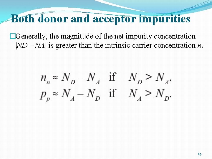
Both donor and acceptor impurities �Generally, the magnitude of the net impurity concentration |ND – NA| is greater than the intrinsic carrier concentration ni 69

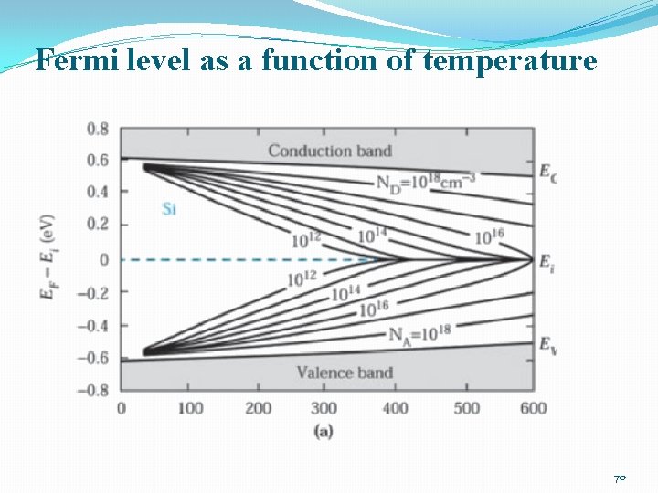
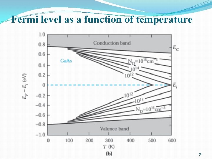
Fermi level as a function of temperature 70

Fermi level as a function of temperature 71

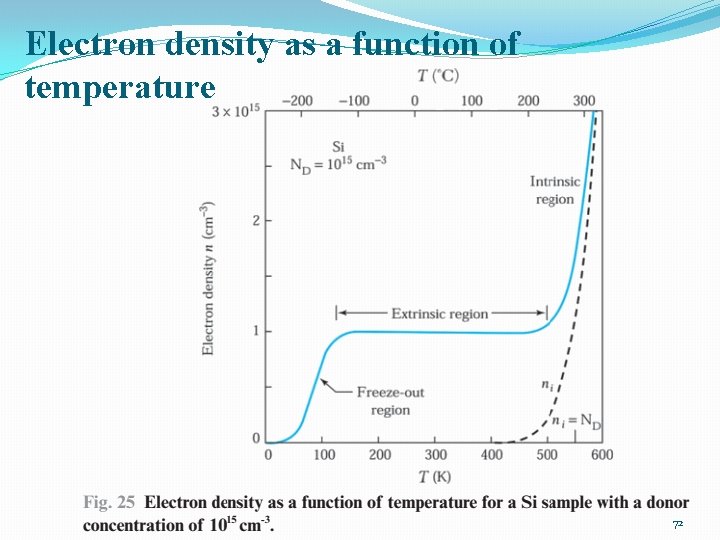
Electron density as a function of temperature 72

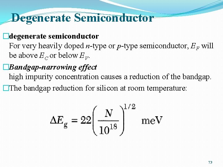
Degenerate Semiconductor �degenerate semiconductor For very heavily doped n-type or p-type semiconductor, EF will be above EC or below EV. �Bandgap-narrowing effect high impurity concentration causes a reduction of the bandgap. �The bandgap reduction for silicon at room temperature: 73