Lecture 16 Pico Blaze IO Interrupt Interface ECE

Lecture 16 Pico. Blaze I/O & Interrupt Interface ECE 448 – FPGA and ASIC Design with VHDL

Required reading • P. Chu, FPGA Prototyping by VHDL Examples Chapter 16, Pico. Blaze I/O Interface Chapter 17, Pico. Blaze Interrupt Interface ECE 448 – FPGA and ASIC Design with VHDL 2

Syntax and Terminology Syntax Example Definition s. X s 7 Value at register 7 KK ab Value ab (in hex) PORT(KK) PORT(2) Input value from port 2 PORT((s. X)) PORT((s 1)) Input value from the port specified by RAM(KK) RAM(4) register s 1 Value from the RAM location 4

Addressing modes Immediate mode SUB s 7, 07 ADDCY s 2, 08 s 7 – 07 s 7 s 2 + 08 + C s 2 Direct mode ADD sa, sf INPUT s 5, 2 a sa + sf sa PORT(2 a) s 5 Indirect mode STORE s 3, (sa) s 3 RAM((sa)) INPUT s 9, (s 2) PORT((s 2)) s 9

Output Decoding of Four Output Registers ECE 448 – FPGA and ASIC Design with VHDL 5
 <=")
Output Instructions C Z OUTPUT s. X, KK DIR −− IND −− PORT(KK) <= s. X OUTPUT s. X, (s. Y) PORT((s. Y)) <= s. X

Timing Diagram of an Output Instruction ECE 448 – FPGA and ASIC Design with VHDL 7

Truth Table of a Decoding Circuit ECE 448 – FPGA and ASIC Design with VHDL 8

Input Instructions C Z INPUT s. X, KK DIR −− IND −− s. X <= PORT(KK) INPUT s. X, (s. Y) s. X <= PORT((s. Y))

Block Diagram of Four Continuous-Access Ports ECE 448 – FPGA and ASIC Design with VHDL 10

Timing Diagram of an Input Instruction ECE 448 – FPGA and ASIC Design with VHDL 11

Block Diagram of Four Single-Access Ports ECE 448 – FPGA and ASIC Design with VHDL 12

FIFO Interface clk rst FIFO din dout 8 8 full write ECE 448 – FPGA and ASIC Design with VHDL empty read 13

Operation of the “Standard” FIFO −−−−− ECE 448 – FPGA and ASIC Design with VHDL A B C D 14

Operation of the First-Word Fall-Through FIFO ECE 448 – FPGA and ASIC Design with VHDL 15

ECE 448 – FPGA and ASIC Design with VHDL 16

Timing Diagram of an Input Instruction ECE 448 – FPGA and ASIC Design with VHDL 17

Interrupt Flow ECE 448 – FPGA and ASIC Design with VHDL 18

Timing Diagram of an Interrupt Event ECE 448 – FPGA and ASIC Design with VHDL 19

ECE 448 – FPGA and ASIC Design with VHDL 20
![Interrupt Related Instructions RETURNI ENABLE PC <= STACK[TOS] ; TOS <= TOS – 1;](http://slidetodoc.com/presentation_image_h2/ff2aae44590d7dbf0a323605d7387c97/image-21.jpg "Interrupt Related Instructions RETURNI ENABLE PC <= STACK[TOS] ; TOS <= TOS – 1;")
Interrupt Related Instructions RETURNI ENABLE PC <= STACK[TOS] ; TOS <= TOS – 1; I <= 1; C<= PRESERVED C; Z<= PRESERVED Z RETURNI DISABLE PC <= STACK[TOS] ; TOS <= TOS – 1; I <= 0; C<= PRESERVED C; Z<= PRESERVED Z ENABLE INTERRUPT I <=1; DISABLE INTERRUPT I <=0;

Interrupt Interface with a Single Event ECE 448 – FPGA and ASIC Design with VHDL 22

Interrupt Interface with Two Requests ECE 448 – FPGA and ASIC Design with VHDL 23

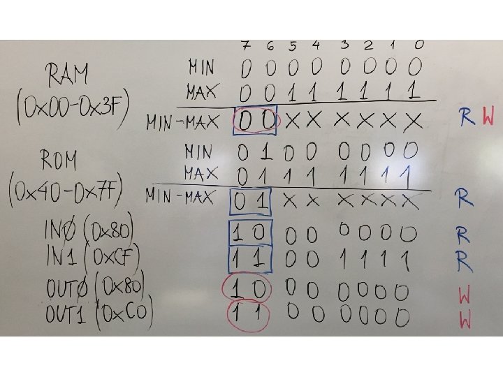
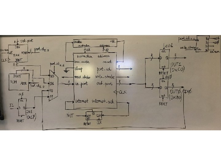
Pico. Blaze Input/Output Class Exercise

Task Draw a detailed block diagram of the digital system including: 1. Pico. Blaze-6, KCPSM 6 2. 4 k x 18 instruction ROM required for the basic operation of Pic 3. 64 x 8 external data RAM visible under addresses 0 x 00 -0 x 3 F 4. 64 x 8 external data ROM visible under addresses 0 x 40 -0 x 7 F 5. two input registers with the virtual addresses 0 x 80 and 0 x. CF 6. two output registers with the virtual addresses 0 x 80 and 0 x. C 0 7. D flip-flop with the output Q connected to the interrupt input of the Pico. Blaze core, input SET connected to the external port IN and input CLR connected to an appropriate output of the Pico. B ECE 448 – FPGA and ASIC Design with VHDL 25

Assumptions • input register with the address 0 x 80 is the same as the output register with the address 0 x 80 • the input and output registers, data RAM, and data ROM specif are the only i/o devices that the Pico. Blaze core is communicatin • your system needs to be able to allow the Pico. Blaze core to wr all aforementioned output registers and data RAM, and read fro all the aforementioned input registers, data RAM, and data ROM using instructions OUTPUT and INPUT, respectively • you need to provide all details of the address decoder, and build out of basic logic components you are familiar with • all registers and flip-flops have a reset input connected to the ex port RESET. ECE 448 – FPGA and ASIC Design with VHDL 26

Requirements Please clearly mark on your schematic: • sizes of all memories and registers • sizes and directions of all buses. ECE 448 – FPGA and ASIC Design with VHDL 27

Interface of Pico. Blaze-6 28

rdl – reset during load The program memory has the option to include the JTAG Loader utility which facilitates rapid developm of your KCPSM 6 program. ‘rdl’ is a ‘reset during load’ signal associated with the loader, which needs to be connected to the reset input of the processor. ECE 448 – FPGA and ASIC Design with VHDL 29

Development Flow of a System with Pico. Blaze ECE 448 – FPGA and ASIC Design with VHDL 30

Pico. Blaze Input/Output Class Exercise Solutions
- Slides: 33