ELEC 52706270 Spring 2013 LowPower Design of Electronic
- Slides: 44

ELEC 5270/6270 Spring 2013 Low-Power Design of Electronic Circuits Memory and Multicore Design Vishwani D. Agrawal James J. Danaher Professor Dept. of Electrical and Computer Engineering Auburn University, Auburn, AL 36849 vagrawal@eng. auburn. edu http: //www. eng. auburn. edu/~vagrawal/COURSE/E 6270_Spr 13/course. html Copyright Agrawal, 2007 ELEC 6270 Spring 13, Lecture 9 1

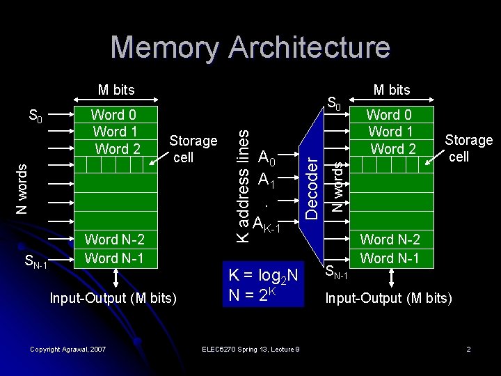
Memory Architecture M bits SN-1 Word N-2 Word N-1 Input-Output (M bits) Copyright Agrawal, 2007 K = log 2 N N = 2 K ELEC 6270 Spring 13, Lecture 9 Word 0 Word 1 Word 2 N words A 0 A 1. AK-1 Decoder Storage cell K address lines Word 0 Word 1 Word 2 N words S 0 M bits SN-1 Storage cell Word N-2 Word N-1 Input-Output (M bits) 2

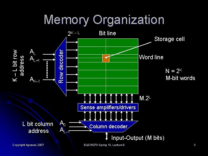
Memory Organization AL AL+1 AK– 1 Bit line Row decoder K – L bit row address 2 K – L Storage cell Word line N = 2 K M-bit words M. 2 L Sense amplifiers/drivers L bit column address A 0 AL– 1 Column decoder Input-Output (M bits) Copyright Agrawal, 2007 ELEC 6270 Spring 13, Lecture 9 3

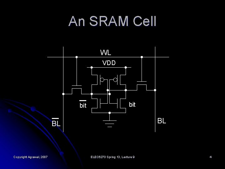
An SRAM Cell WL VDD bit BL BL Copyright Agrawal, 2007 ELEC 6270 Spring 13, Lecture 9 4

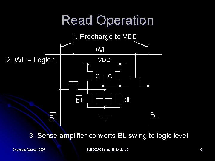
Read Operation 1. Precharge to VDD WL 2. WL = Logic 1 VDD bit BL BL 3. Sense amplifier converts BL swing to logic level Copyright Agrawal, 2007 ELEC 6270 Spring 13, Lecture 9 5

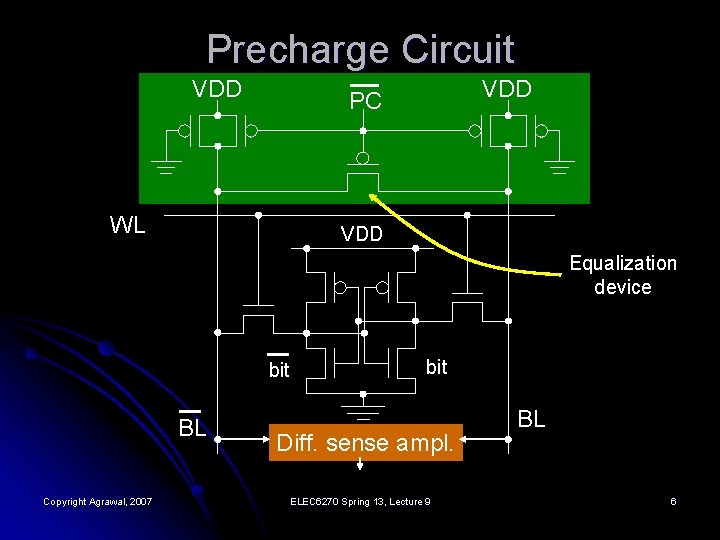
Precharge Circuit VDD PC WL VDD Equalization device bit BL Copyright Agrawal, 2007 bit Diff. sense ampl. ELEC 6270 Spring 13, Lecture 9 BL 6

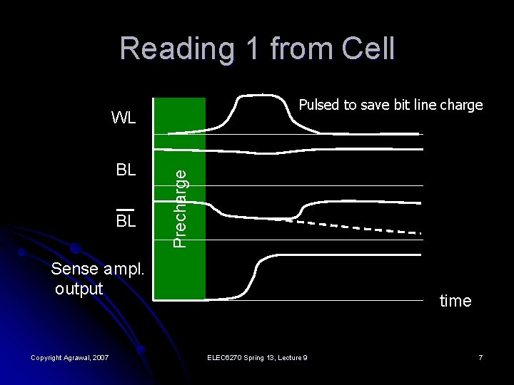
Reading 1 from Cell Pulsed to save bit line charge BL BL Precharge WL Sense ampl. output Copyright Agrawal, 2007 time ELEC 6270 Spring 13, Lecture 9 7

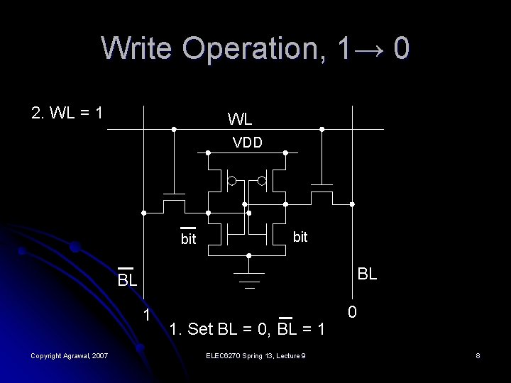
Write Operation, 1→ 0 2. WL = 1 WL VDD bit BL BL 1 Copyright Agrawal, 2007 1. Set BL = 0, BL = 1 ELEC 6270 Spring 13, Lecture 9 0 8

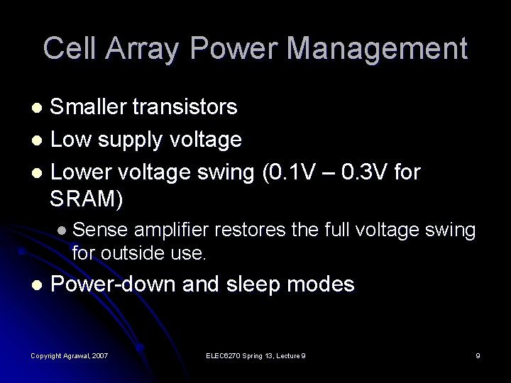
Cell Array Power Management Smaller transistors l Low supply voltage l Lower voltage swing (0. 1 V – 0. 3 V for SRAM) l l Sense amplifier restores the full voltage swing for outside use. l Power-down and sleep modes Copyright Agrawal, 2007 ELEC 6270 Spring 13, Lecture 9 9

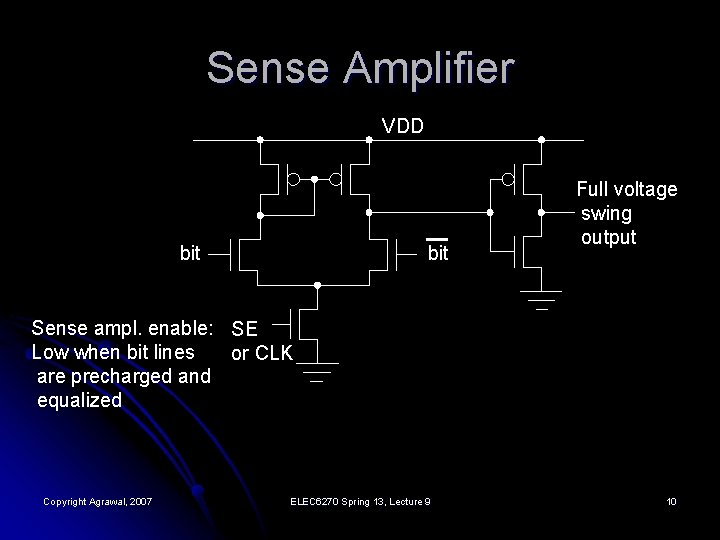
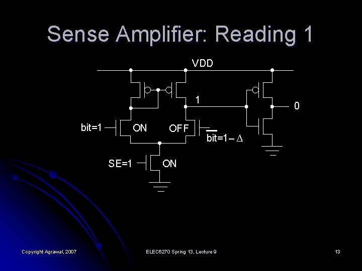
Sense Amplifier VDD bit Full voltage swing output Sense ampl. enable: SE Low when bit lines or CLK are precharged and equalized Copyright Agrawal, 2007 ELEC 6270 Spring 13, Lecture 9 10

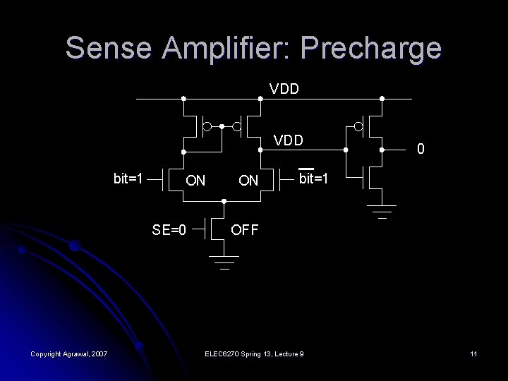
Sense Amplifier: Precharge VDD bit=1 ON SE=0 Copyright Agrawal, 2007 ON 0 bit=1 OFF ELEC 6270 Spring 13, Lecture 9 11

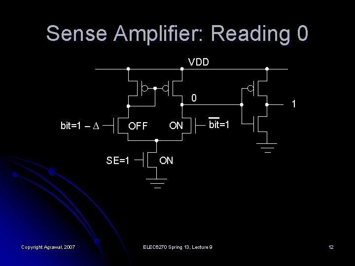
Sense Amplifier: Reading 0 VDD 0 bit=1 – ∆ OFF SE=1 Copyright Agrawal, 2007 ON 1 bit=1 ON ELEC 6270 Spring 13, Lecture 9 12

Sense Amplifier: Reading 1 VDD 1 bit=1 ON SE=1 Copyright Agrawal, 2007 OFF 0 bit=1– ∆ ON ELEC 6270 Spring 13, Lecture 9 13

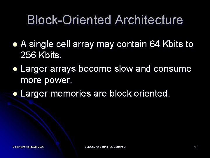
Block-Oriented Architecture A single cell array may contain 64 Kbits to 256 Kbits. l Larger arrays become slow and consume more power. l Larger memories are block oriented. l Copyright Agrawal, 2007 ELEC 6270 Spring 13, Lecture 9 14

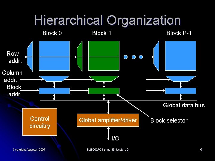
Hierarchical Organization Block 0 Block 1 Block P-1 Row addr. Column addr. Block addr. Global data bus Control circuitry Global amplifier/driver Block selector I/O Copyright Agrawal, 2007 ELEC 6270 Spring 13, Lecture 9 15

Power Saving l Block-oriented memory l Lengths of local word and bit lines are kept small. l Block address is used to activate the addressed block. l Unaddressed blocks are put in power-saving mode: sense amplifier and row/column decoders are disabled. l Cell array is put in power-saving mode. l Copyright Agrawal, 2007 ELEC 6270 Spring 13, Lecture 9 16

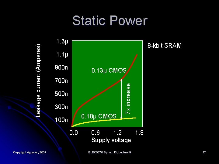
1. 3μ 8 -kbit SRAM 1. 1μ 900 n 0. 13μ CMOS 700 n 500 n 300 n 0. 18μ CMOS 100 n 0. 0 Copyright Agrawal, 2007 7 x increase Leakage current (Amperes) Static Power 0. 6 1. 2 1. 8 Supply voltage ELEC 6270 Spring 13, Lecture 9 17

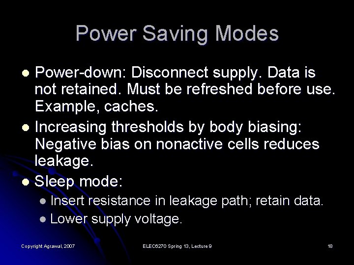
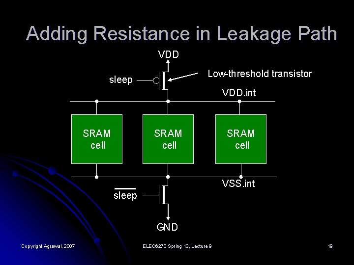
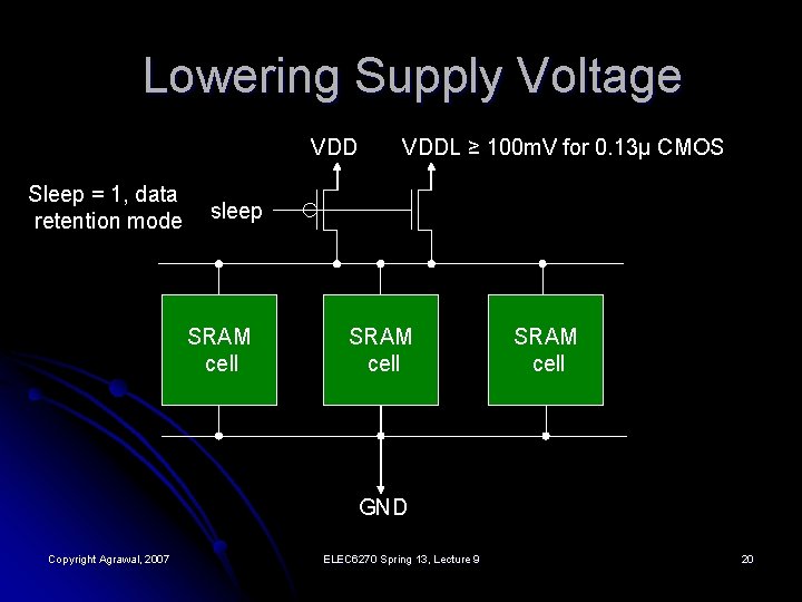
Power Saving Modes Power-down: Disconnect supply. Data is not retained. Must be refreshed before use. Example, caches. l Increasing thresholds by body biasing: Negative bias on nonactive cells reduces leakage. l Sleep mode: l l Insert resistance in leakage path; retain data. l Lower supply voltage. Copyright Agrawal, 2007 ELEC 6270 Spring 13, Lecture 9 18

Adding Resistance in Leakage Path VDD Low-threshold transistor sleep VDD. int SRAM cell VSS. int sleep GND Copyright Agrawal, 2007 ELEC 6270 Spring 13, Lecture 9 19

Lowering Supply Voltage VDD Sleep = 1, data retention mode VDDL ≥ 100 m. V for 0. 13μ CMOS sleep SRAM cell GND Copyright Agrawal, 2007 ELEC 6270 Spring 13, Lecture 9 20

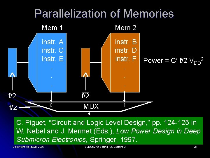
Parallelization of Memories Mem 1 Mem 2 instr. A instr. C instr. E. . . instr. B instr. D instr. F Power = C’ f/2 V 2 DD. . . f/2 f/2 0 MUX 1 C. Piguet, “Circuit and Logic Level Design, ” pp. 124 -125 in W. Nebel and J. Mermet (Eds. ), Low Power Design in Deep Submicron Electronics, Springer, 1997. Copyright Agrawal, 2007 ELEC 6270 Spring 13, Lecture 9 21

References l l l K. Itoh, VLSI Memory Chip Design, Springer. Verlag, 2001. J. M. Rabaey, A. Chandrakasan and B. Nikolić, Digital Integrated Circuits, Upper Saddle River, New Jersey: Pearson Education, Inc. , 2003, Chapter 12. S. -M. Kang and Y. Leblebici, CMOS Digital Integrated Circuits Analysis and Design, New York: Mc. Graw-Hill, 1996, Chapter 10. Copyright Agrawal, 2007 ELEC 6270 Spring 13, Lecture 9 22

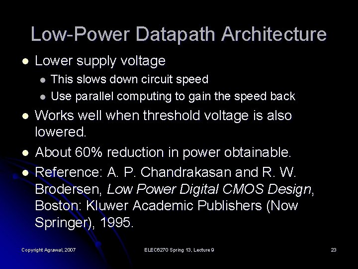
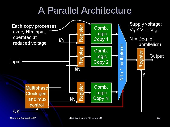
Low-Power Datapath Architecture l Lower supply voltage l l l This slows down circuit speed Use parallel computing to gain the speed back Works well when threshold voltage is also lowered. About 60% reduction in power obtainable. Reference: A. P. Chandrakasan and R. W. Brodersen, Low Power Digital CMOS Design, Boston: Kluwer Academic Publishers (Now Springer), 1995. Copyright Agrawal, 2007 ELEC 6270 Spring 13, Lecture 9 23

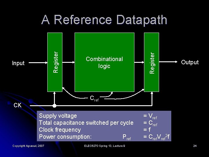
Input Combinational logic Register A Reference Datapath Output Cref CK Supply voltage Total capacitance switched per cycle Clock frequency Power consumption: Pref Copyright Agrawal, 2007 ELEC 6270 Spring 13, Lecture 9 = Vref = Cref =f = Cref. Vref 2 f 24

Comb. Logic Copy 2 Multiphase Clock gen. and mux control f/N Register f/N N = Deg. of parallelism Register Comb. Logic Copy 1 Supply voltage: VN ≤ V 1 = Vref N to 1 multiplexer Input Register Each copy processes every Nth input, operates at f/N reduced voltage Register A Parallel Architecture Output f Comb. Logic Copy N CK Copyright Agrawal, 2007 ELEC 6270 Spring 13, Lecture 9 25

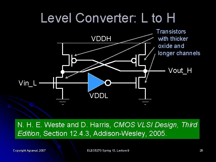
Level Converter: L to H VDDH Transistors with thicker oxide and longer channels Vout_H Vin_L VDDL N. H. E. Weste and D. Harris, CMOS VLSI Design, Third Edition, Section 12. 4. 3, Addison-Wesley, 2005. Copyright Agrawal, 2007 ELEC 6270 Spring 13, Lecture 9 26

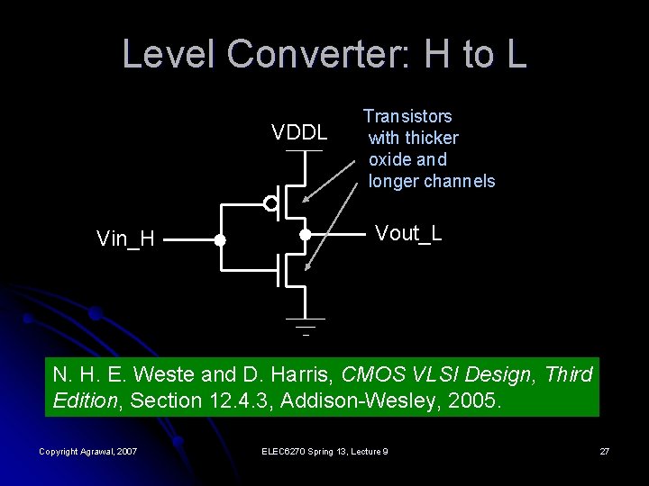
Level Converter: H to L VDDL Vin_H Transistors with thicker oxide and longer channels Vout_L N. H. E. Weste and D. Harris, CMOS VLSI Design, Third Edition, Section 12. 4. 3, Addison-Wesley, 2005. Copyright Agrawal, 2007 ELEC 6270 Spring 13, Lecture 9 27

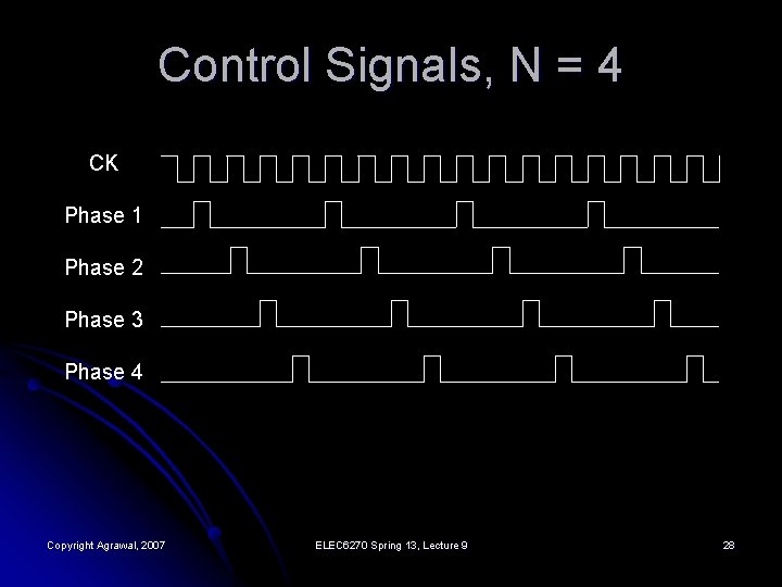
Control Signals, N = 4 CK Phase 1 Phase 2 Phase 3 Phase 4 Copyright Agrawal, 2007 ELEC 6270 Spring 13, Lecture 9 28

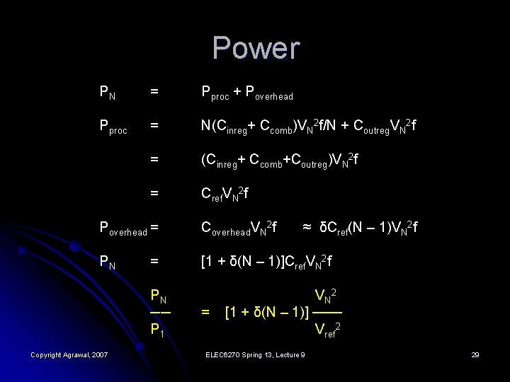
Power PN = Pproc + Poverhead Pproc = N(Cinreg+ Ccomb)VN 2 f/N + Coutreg. VN 2 f = (Cinreg+ Ccomb+Coutreg)VN 2 f = Cref. VN 2 f Poverhead = Coverhead. VN 2 f PN [1 + δ(N – 1)]Cref. VN 2 f = PN ── P 1 Copyright Agrawal, 2007 = ≈ δCref(N – 1)VN 2 f VN 2 [1 + δ(N – 1)] ─── Vref 2 ELEC 6270 Spring 13, Lecture 9 29

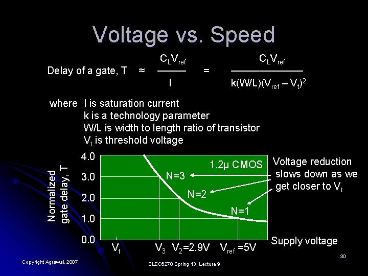
Voltage vs. Speed Delay of a gate, T ≈ CLVref ──── I CLVref ───── k(W/L)(Vref – Vt)2 = where I is saturation current k is a technology parameter W/L is width to length ratio of transistor Vt is threshold voltage Normalized gate delay, T 4. 0 N=2 2. 0 N=1 1. 0 0. 0 Copyright Agrawal, 2007 N=3 3. 0 1. 2μ CMOS Voltage reduction slows down as we get closer to Vt Vt V 3 V 2=2. 9 V Vref =5 V ELEC 6270 Spring 13, Lecture 9 Supply voltage 30

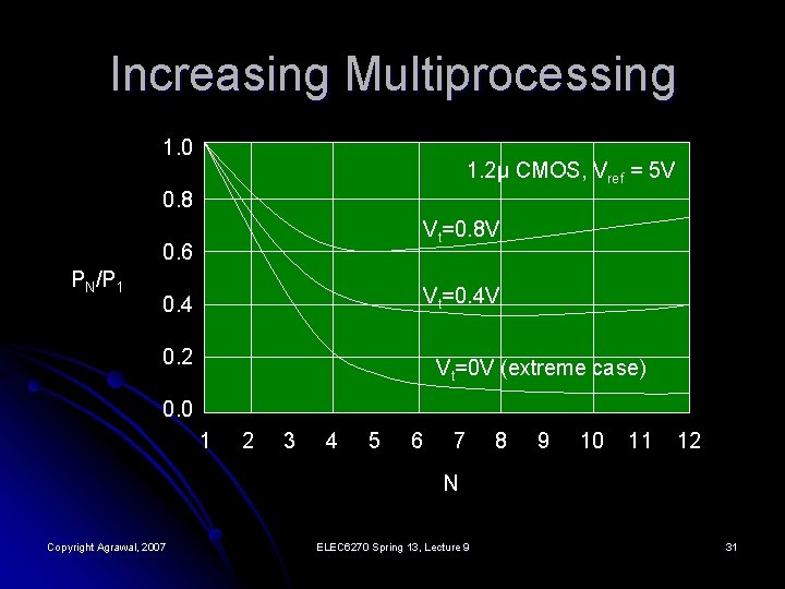
Increasing Multiprocessing 1. 0 1. 2μ CMOS, Vref = 5 V 0. 8 Vt=0. 8 V 0. 6 PN/P 1 Vt=0. 4 V 0. 4 0. 2 Vt=0 V (extreme case) 0. 0 1 2 3 4 5 6 7 8 9 10 11 12 N Copyright Agrawal, 2007 ELEC 6270 Spring 13, Lecture 9 31

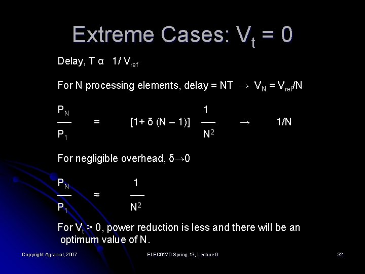
Extreme Cases: Vt = 0 Delay, T α 1/ Vref For N processing elements, delay = NT → VN = Vref/N PN ── P 1 = [1+ δ (N – 1)] 1 ── N 2 → 1/N For negligible overhead, δ→ 0 PN ── P 1 ≈ 1 ── N 2 For Vt > 0, power reduction is less and there will be an optimum value of N. Copyright Agrawal, 2007 ELEC 6270 Spring 13, Lecture 9 32

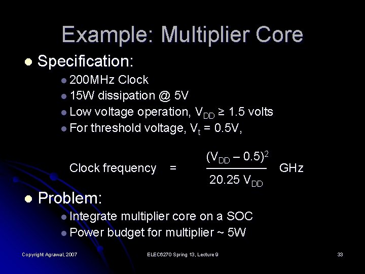
Example: Multiplier Core l Specification: l 200 MHz Clock l 15 W dissipation @ 5 V l Low voltage operation, VDD ≥ 1. 5 volts l For threshold voltage, Vt = 0. 5 V, Clock frequency l = (VDD – 0. 5)2 ─────── GHz 20. 25 VDD Problem: l Integrate multiplier core on a SOC l Power budget for multiplier ~ 5 W Copyright Agrawal, 2007 ELEC 6270 Spring 13, Lecture 9 33

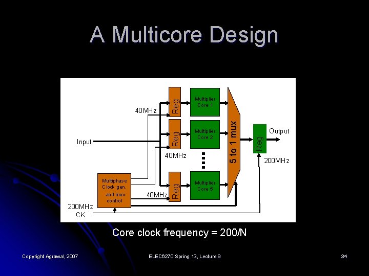
Input Multiplier Core 2 200 MHz CK Multiphase Clock gen. and mux control 40 MHz Reg 40 MHz Output Reg 40 MHz Multiplier Core 1 5 to 1 mux Reg A Multicore Design 200 MHz Multiplier Core 5 Core clock frequency = 200/N Copyright Agrawal, 2007 ELEC 6270 Spring 13, Lecture 9 34

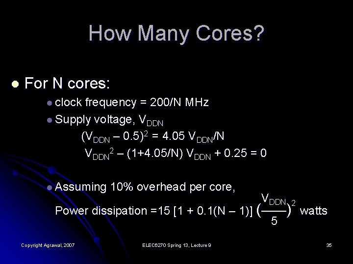
How Many Cores? l For N cores: l clock frequency = 200/N MHz l Supply voltage, VDDN (VDDN – 0. 5)2 = 4. 05 VDDN/N VDDN 2 – (1+4. 05/N) VDDN + 0. 25 = 0 l Assuming 10% overhead per core, VDDN 2 Power dissipation =15 [1 + 0. 1(N – 1)] (───) watts 5 Copyright Agrawal, 2007 ELEC 6270 Spring 13, Lecture 9 35

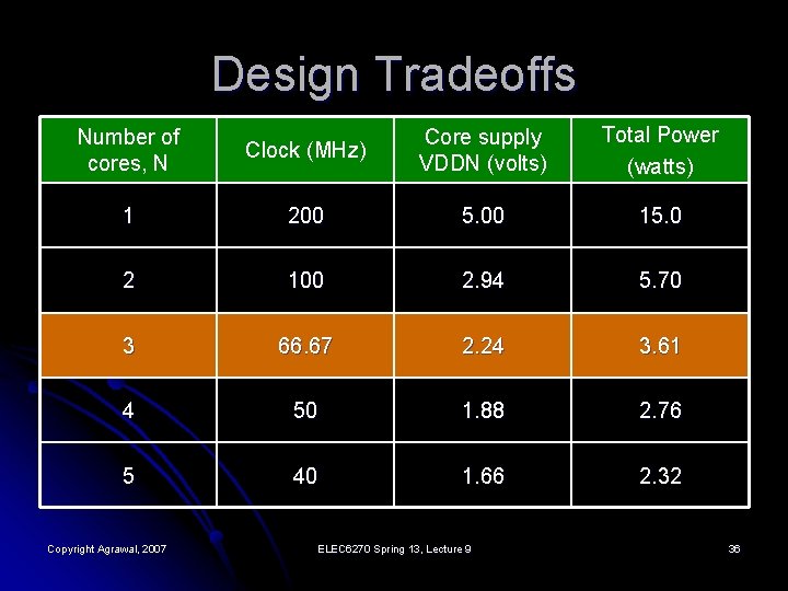
Design Tradeoffs Clock (MHz) Core supply VDDN (volts) Total Power (watts) 1 200 5. 00 15. 0 2 100 2. 94 5. 70 3 66. 67 2. 24 3. 61 4 50 1. 88 2. 76 5 40 1. 66 2. 32 Number of cores, N Copyright Agrawal, 2007 ELEC 6270 Spring 13, Lecture 9 36

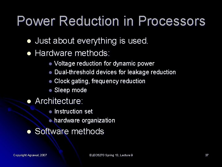
Power Reduction in Processors l l Just about everything is used. Hardware methods: Voltage reduction for dynamic power l Dual-threshold devices for leakage reduction l Clock gating, frequency reduction l Sleep mode l l Architecture: Instruction set l hardware organization l l Software methods Copyright Agrawal, 2007 ELEC 6270 Spring 13, Lecture 9 37

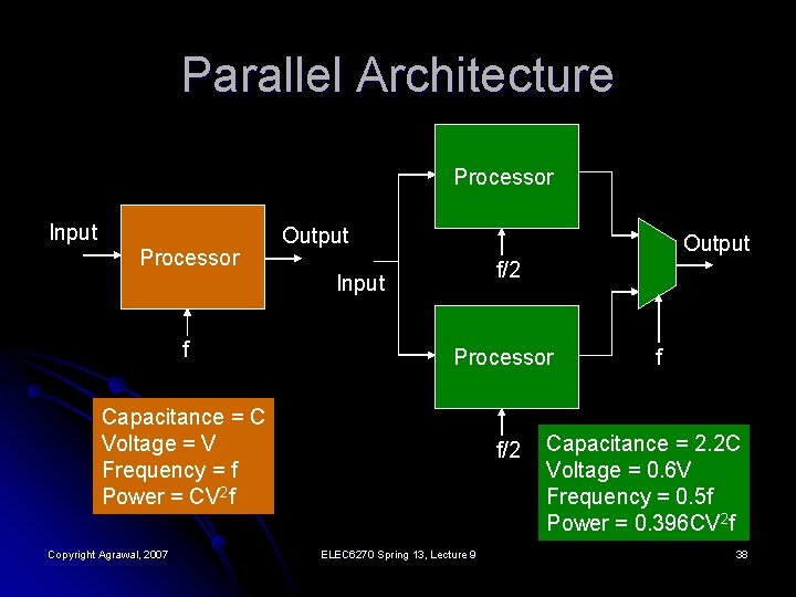
Parallel Architecture Processor Input Processor Output f/2 Input f Processor Capacitance = C Voltage = V Frequency = f Power = CV 2 f f/2 Copyright Agrawal, 2007 ELEC 6270 Spring 13, Lecture 9 f Capacitance = 2. 2 C Voltage = 0. 6 V Frequency = 0. 5 f Power = 0. 396 CV 2 f 38

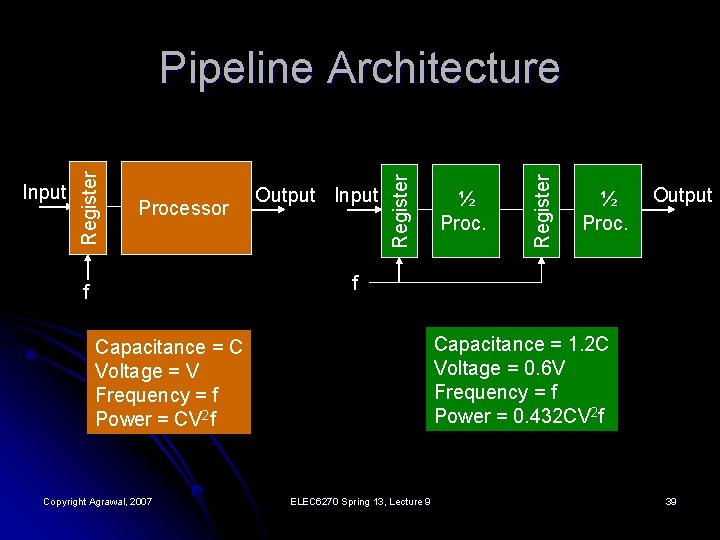
Output Input ½ Proc. Register Processor Register Input Register Pipeline Architecture ½ Proc. Output f f Capacitance = 1. 2 C Voltage = 0. 6 V Frequency = f Power = 0. 432 CV 2 f Capacitance = C Voltage = V Frequency = f Power = CV 2 f Copyright Agrawal, 2007 ELEC 6270 Spring 13, Lecture 9 39

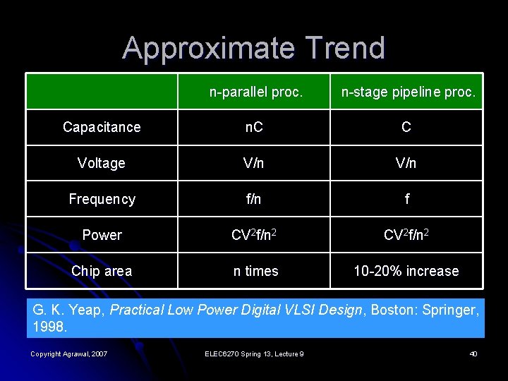
Approximate Trend n-parallel proc. n-stage pipeline proc. Capacitance n. C C Voltage V/n Frequency f/n f Power CV 2 f/n 2 Chip area n times 10 -20% increase G. K. Yeap, Practical Low Power Digital VLSI Design, Boston: Springer, 1998. Copyright Agrawal, 2007 ELEC 6270 Spring 13, Lecture 9 40

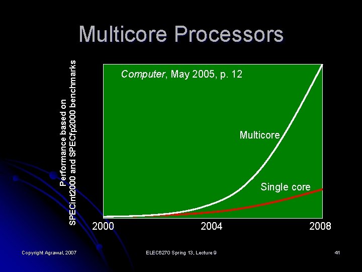
Performance based on SPECint 2000 and SPECfp 2000 benchmarks Multicore Processors Copyright Agrawal, 2007 Computer, May 2005, p. 12 Multicore Single core 2000 2004 ELEC 6270 Spring 13, Lecture 9 2008 41

Multicore Processors l l l D. Geer, “Chip Makers Turn to Multicore Processors, ” Computer, vol. 38, no. 5, pp. 11 -13, May 2005. A. Jerraya, H. Tenhunen and W. Wolf, “Multiprocessor Systems-on-Chips, ” Computer, vol. 5, no. 7, pp. 36 -40, July 2005; this special issue contains three more articles on multicore processors. S. K. Moore, “Winner Multimedia Monster – Cell’s Nine Processors Make It a Supercomputer on a Chip, ” IEEE Spectrum, vol. 43. no. 1, pp. 20 -23, January 2006. Copyright Agrawal, 2007 ELEC 6270 Spring 13, Lecture 9 42

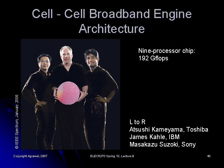
Cell - Cell Broadband Engine Architecture © IEEE Spectrum, January 2006 Nine-processor chip: 192 Gflops Copyright Agrawal, 2007 L to R Atsushi Kameyama, Toshiba James Kahle, IBM Masakazu Suzoki, Sony ELEC 6270 Spring 13, Lecture 9 43

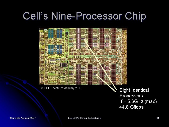
Cell’s Nine-Processor Chip © IEEE Spectrum, January 2006 Copyright Agrawal, 2007 ELEC 6270 Spring 13, Lecture 9 Eight Identical Processors f = 5. 6 GHz (max) 44. 8 Gflops 44