ELEC 52706270 Spring 2009 LowPower Design of Electronic
- Slides: 44

ELEC 5270/6270 Spring 2009 Low-Power Design of Electronic Circuits Memory and Multicore Design Vishwani D. Agrawal James J. Danaher Professor Dept. of Electrical and Computer Engineering Auburn University, Auburn, AL 36849 vagrawal@eng. auburn. edu http: //www. eng. auburn. edu/~vagrawal/COURSE/E 6270_Spr 09/course. html Copyright Agrawal, 2007 ELEC 6270 Spring 09, Lecture 11 1

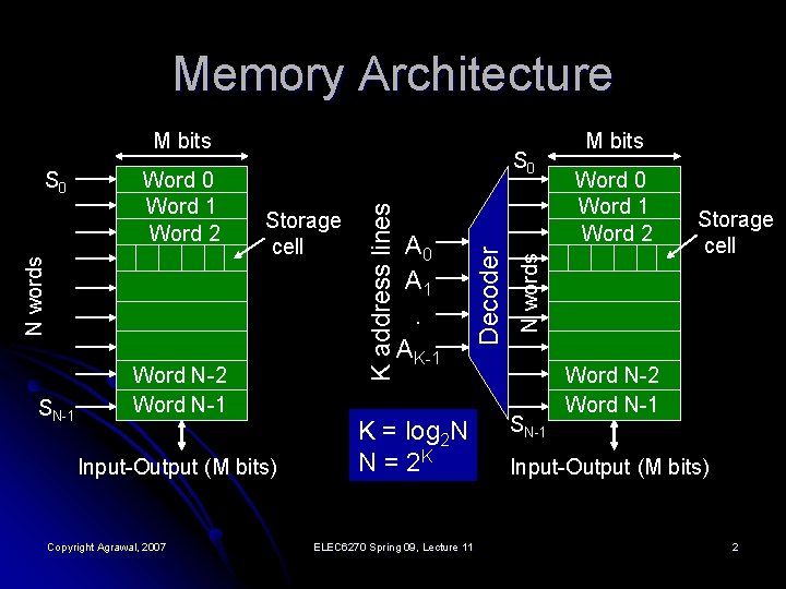
Memory Architecture M bits SN-1 Word N-2 Word N-1 Input-Output (M bits) Copyright Agrawal, 2007 K = log 2 N N = 2 K ELEC 6270 Spring 09, Lecture 11 Word 0 Word 1 Word 2 N words A 0 A 1. AK-1 Decoder Storage cell K address lines Word 0 Word 1 Word 2 N words S 0 M bits SN-1 Storage cell Word N-2 Word N-1 Input-Output (M bits) 2

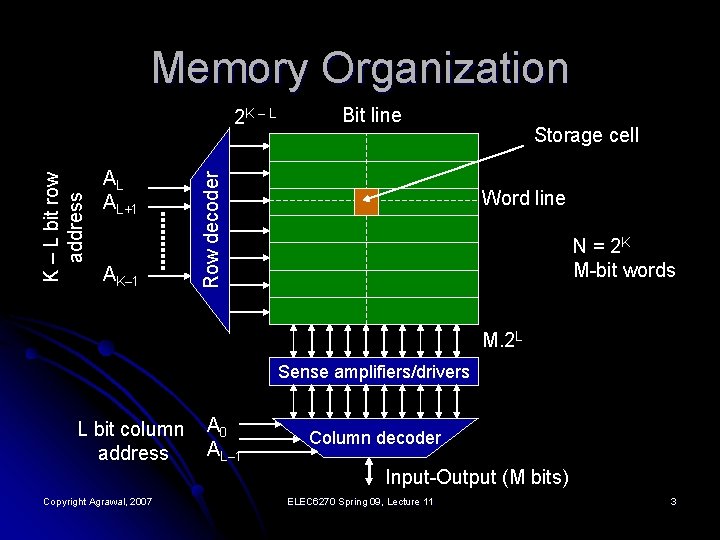
Memory Organization AL AL+1 AK– 1 Bit line Row decoder K – L bit row address 2 K – L Storage cell Word line N = 2 K M-bit words M. 2 L Sense amplifiers/drivers L bit column address A 0 AL– 1 Column decoder Input-Output (M bits) Copyright Agrawal, 2007 ELEC 6270 Spring 09, Lecture 11 3

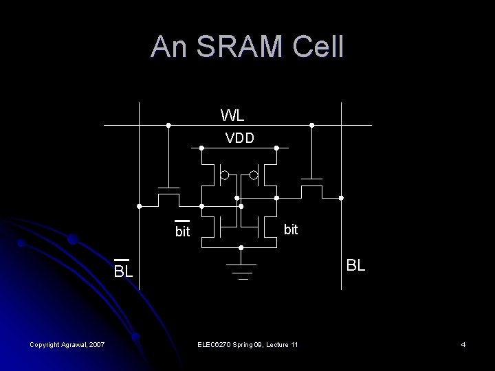
An SRAM Cell WL VDD bit BL BL Copyright Agrawal, 2007 ELEC 6270 Spring 09, Lecture 11 4

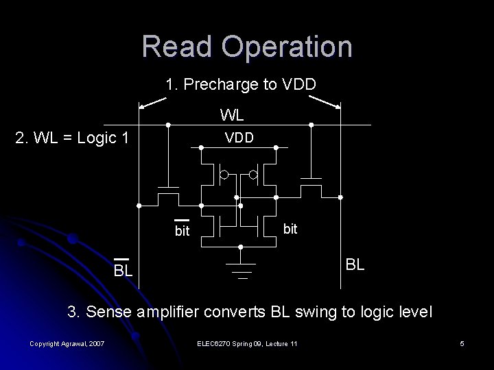
Read Operation 1. Precharge to VDD WL 2. WL = Logic 1 VDD bit BL BL 3. Sense amplifier converts BL swing to logic level Copyright Agrawal, 2007 ELEC 6270 Spring 09, Lecture 11 5

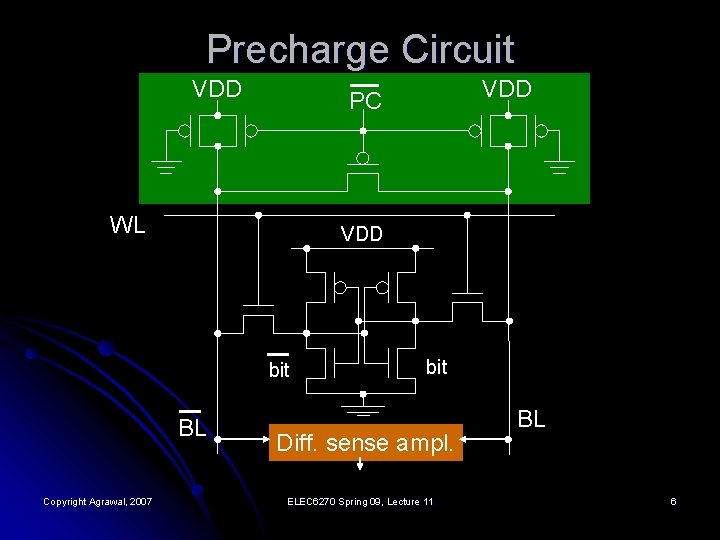
Precharge Circuit VDD WL VDD bit BL Copyright Agrawal, 2007 VDD PC bit Diff. sense ampl. ELEC 6270 Spring 09, Lecture 11 BL 6

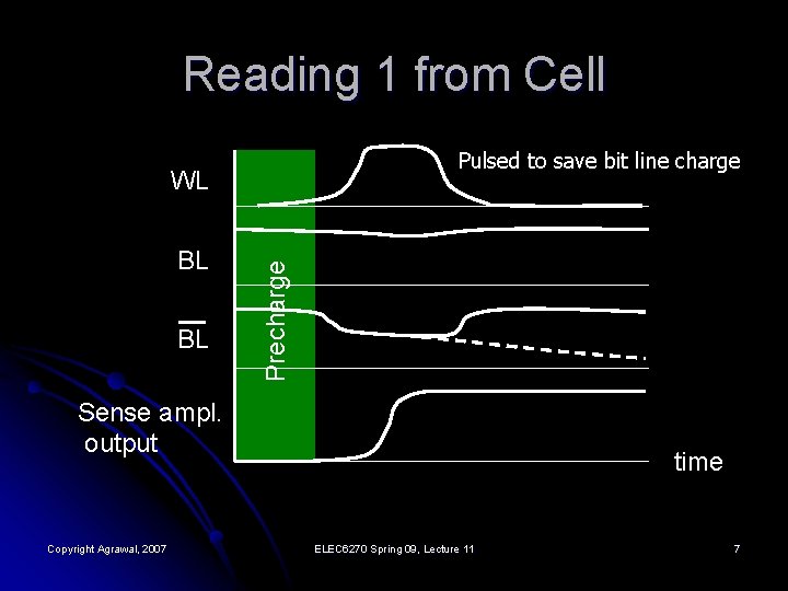
Reading 1 from Cell Pulsed to save bit line charge BL BL Precharge WL Sense ampl. output Copyright Agrawal, 2007 time ELEC 6270 Spring 09, Lecture 11 7

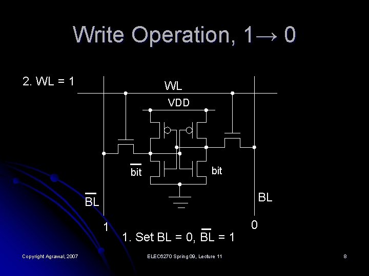
Write Operation, 1→ 0 2. WL = 1 WL VDD bit BL BL 1 Copyright Agrawal, 2007 1. Set BL = 0, BL = 1 ELEC 6270 Spring 09, Lecture 11 0 8

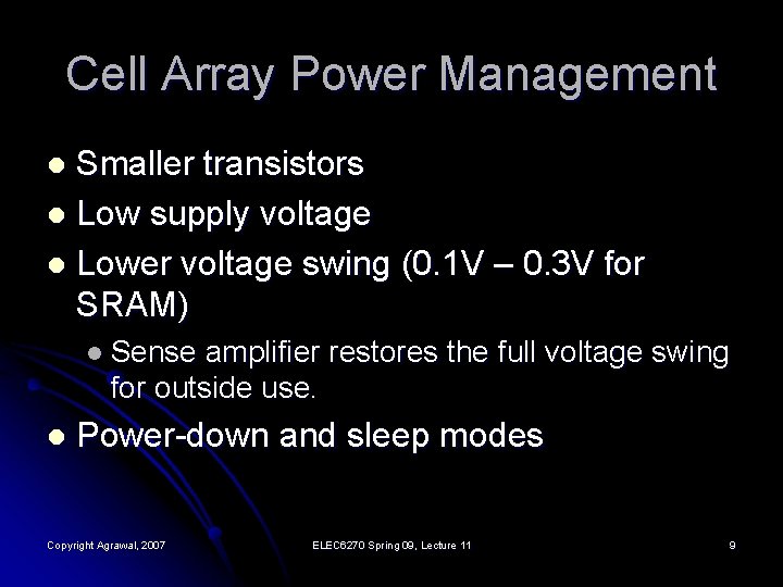
Cell Array Power Management Smaller transistors l Low supply voltage l Lower voltage swing (0. 1 V – 0. 3 V for SRAM) l l Sense amplifier restores the full voltage swing for outside use. l Power-down and sleep modes Copyright Agrawal, 2007 ELEC 6270 Spring 09, Lecture 11 9

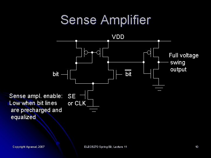
Sense Amplifier VDD bit Full voltage swing output Sense ampl. enable: SE Low when bit lines or CLK are precharged and equalized Copyright Agrawal, 2007 ELEC 6270 Spring 09, Lecture 11 10

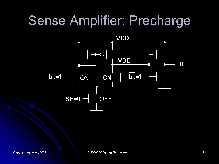
Sense Amplifier: Precharge VDD bit=1 ON SE=0 Copyright Agrawal, 2007 ON 0 bit=1 OFF ELEC 6270 Spring 09, Lecture 11 11

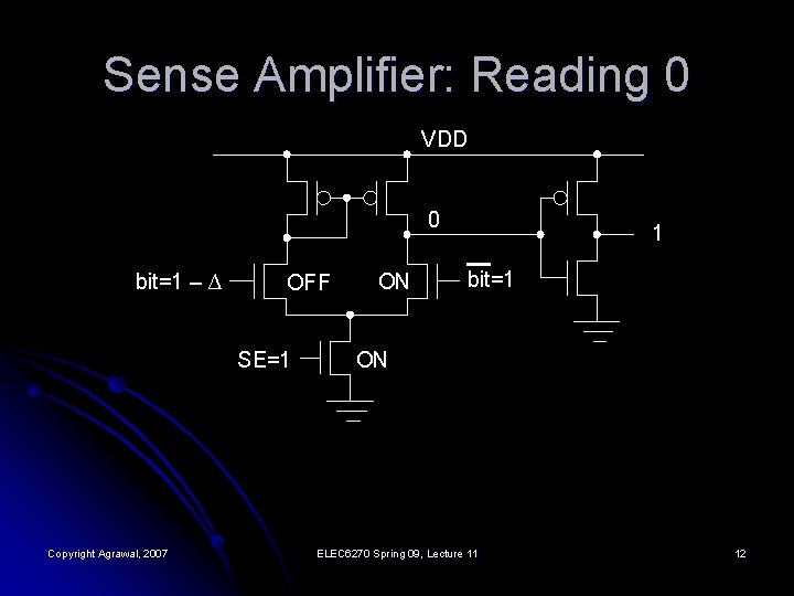
Sense Amplifier: Reading 0 VDD 0 bit=1 – ∆ OFF SE=1 Copyright Agrawal, 2007 ON 1 bit=1 ON ELEC 6270 Spring 09, Lecture 11 12

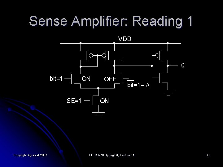
Sense Amplifier: Reading 1 VDD 1 bit=1 ON SE=1 Copyright Agrawal, 2007 OFF 0 bit=1– ∆ ON ELEC 6270 Spring 09, Lecture 11 13

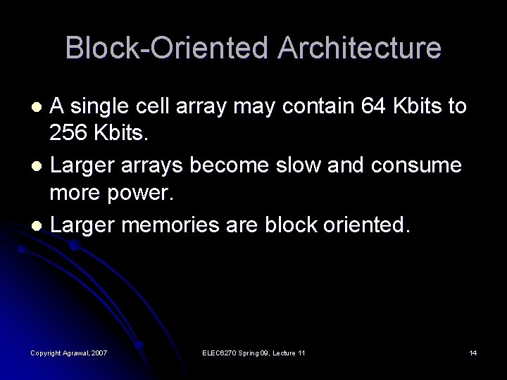
Block-Oriented Architecture A single cell array may contain 64 Kbits to 256 Kbits. l Larger arrays become slow and consume more power. l Larger memories are block oriented. l Copyright Agrawal, 2007 ELEC 6270 Spring 09, Lecture 11 14

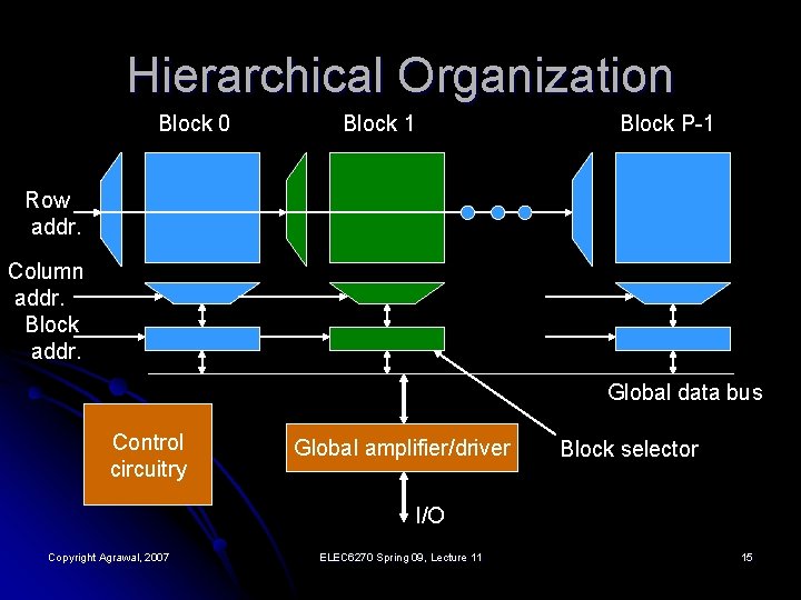
Hierarchical Organization Block 0 Block 1 Block P-1 Row addr. Column addr. Block addr. Global data bus Control circuitry Global amplifier/driver Block selector I/O Copyright Agrawal, 2007 ELEC 6270 Spring 09, Lecture 11 15

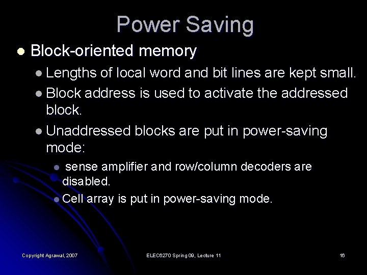
Power Saving l Block-oriented memory l Lengths of local word and bit lines are kept small. l Block address is used to activate the addressed block. l Unaddressed blocks are put in power-saving mode: sense amplifier and row/column decoders are disabled. l Cell array is put in power-saving mode. l Copyright Agrawal, 2007 ELEC 6270 Spring 09, Lecture 11 16

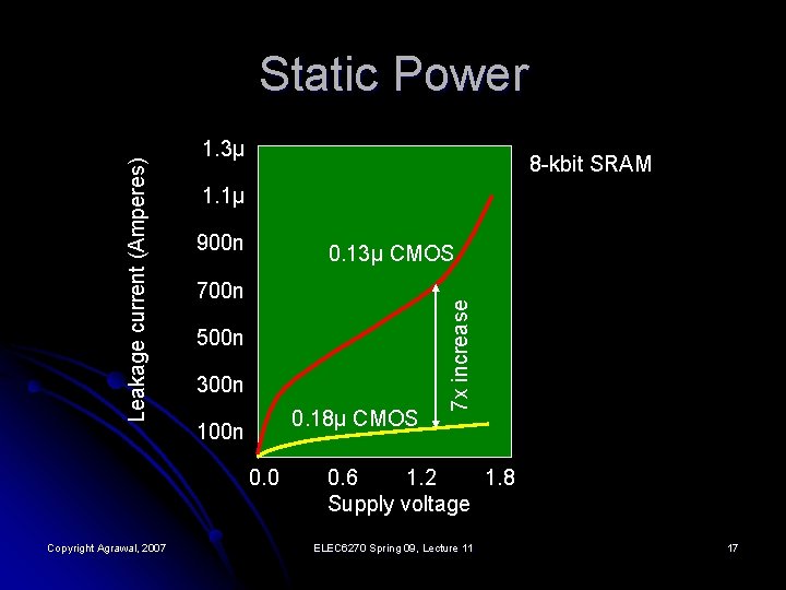
1. 3μ 8 -kbit SRAM 1. 1μ 900 n 0. 13μ CMOS 700 n 500 n 300 n 0. 18μ CMOS 100 n 0. 0 Copyright Agrawal, 2007 7 x increase Leakage current (Amperes) Static Power 0. 6 1. 2 1. 8 Supply voltage ELEC 6270 Spring 09, Lecture 11 17

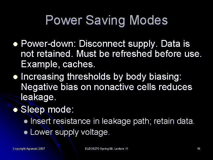
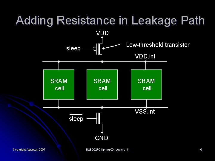
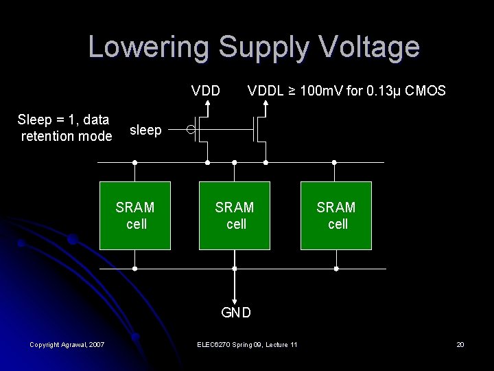
Power Saving Modes Power-down: Disconnect supply. Data is not retained. Must be refreshed before use. Example, caches. l Increasing thresholds by body biasing: Negative bias on nonactive cells reduces leakage. l Sleep mode: l l Insert resistance in leakage path; retain data. l Lower supply voltage. Copyright Agrawal, 2007 ELEC 6270 Spring 09, Lecture 11 18

Adding Resistance in Leakage Path VDD Low-threshold transistor sleep VDD. int SRAM cell VSS. int sleep GND Copyright Agrawal, 2007 ELEC 6270 Spring 09, Lecture 11 19

Lowering Supply Voltage VDD Sleep = 1, data retention mode VDDL ≥ 100 m. V for 0. 13μ CMOS sleep SRAM cell GND Copyright Agrawal, 2007 ELEC 6270 Spring 09, Lecture 11 20

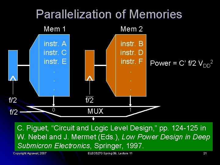
Parallelization of Memories Mem 1 Mem 2 instr. A instr. C instr. E. . . instr. B instr. D instr. F Power = C’ f/2 V 2 DD. . . f/2 f/2 0 MUX 1 C. Piguet, “Circuit and Logic Level Design, ” pp. 124 -125 in W. Nebel and J. Mermet (Eds. ), Low Power Design in Deep Submicron Electronics, Springer, 1997. Copyright Agrawal, 2007 ELEC 6270 Spring 09, Lecture 11 21

References l l l K. Itoh, VLSI Memory Chip Design, Springer. Verlag, 2001. J. M. Rabaey, A. Chandrakasan and B. Nikolić, Digital Integrated Circuits, Upper Saddle River, New Jersey: Pearson Education, Inc. , 2003, Chapter 12. S. -M. Kang and Y. Leblebici, CMOS Digital Integrated Circuits Analysis and Design, New York: Mc. Graw-Hill, 1996, Chapter 10. Copyright Agrawal, 2007 ELEC 6270 Spring 09, Lecture 11 22

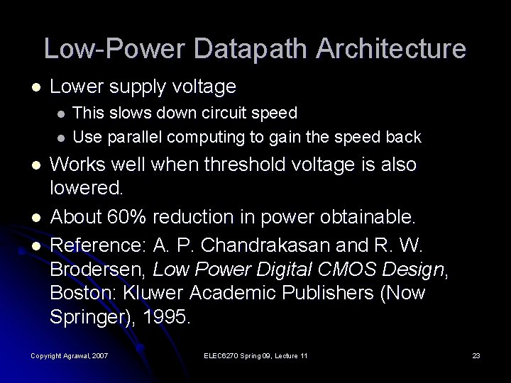
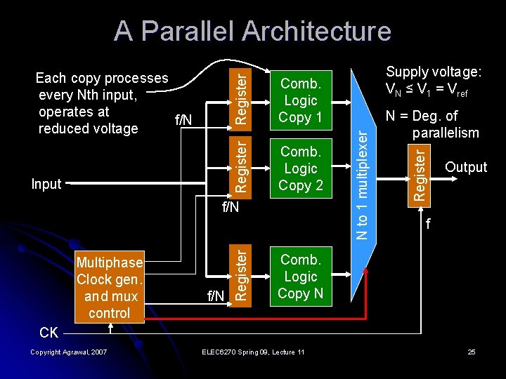
Low-Power Datapath Architecture l Lower supply voltage l l l This slows down circuit speed Use parallel computing to gain the speed back Works well when threshold voltage is also lowered. About 60% reduction in power obtainable. Reference: A. P. Chandrakasan and R. W. Brodersen, Low Power Digital CMOS Design, Boston: Kluwer Academic Publishers (Now Springer), 1995. Copyright Agrawal, 2007 ELEC 6270 Spring 09, Lecture 11 23

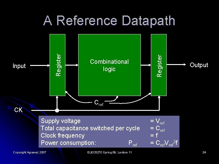
Input Combinational logic Register A Reference Datapath Output Cref CK Supply voltage Total capacitance switched per cycle Clock frequency Power consumption: Pref Copyright Agrawal, 2007 ELEC 6270 Spring 09, Lecture 11 = Vref = Cref =f = Cref. Vref 2 f 24

Comb. Logic Copy 2 Multiphase Clock gen. and mux control f/N Register f/N N = Deg. of parallelism Register Comb. Logic Copy 1 Supply voltage: VN ≤ V 1 = Vref N to 1 multiplexer Input Register Each copy processes every Nth input, operates at f/N reduced voltage Register A Parallel Architecture Output f Comb. Logic Copy N CK Copyright Agrawal, 2007 ELEC 6270 Spring 09, Lecture 11 25

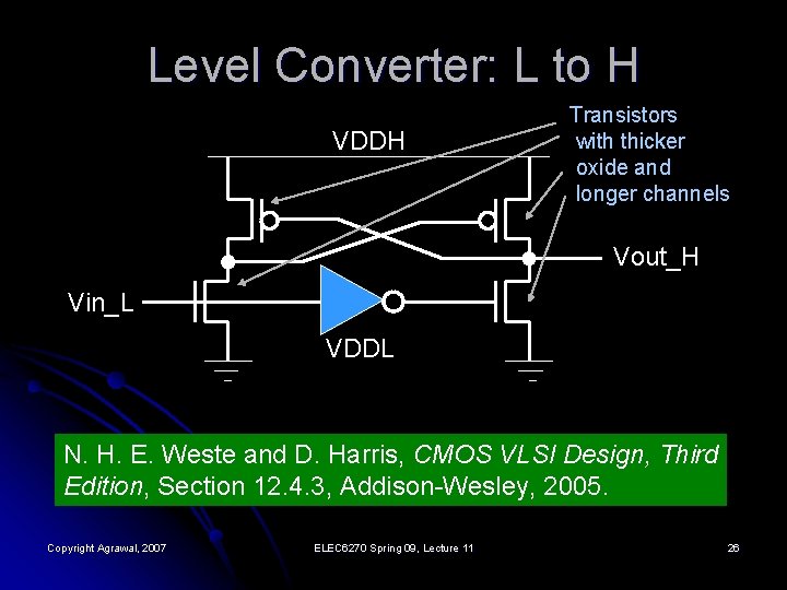
Level Converter: L to H VDDH Transistors with thicker oxide and longer channels Vout_H Vin_L VDDL N. H. E. Weste and D. Harris, CMOS VLSI Design, Third Edition, Section 12. 4. 3, Addison-Wesley, 2005. Copyright Agrawal, 2007 ELEC 6270 Spring 09, Lecture 11 26

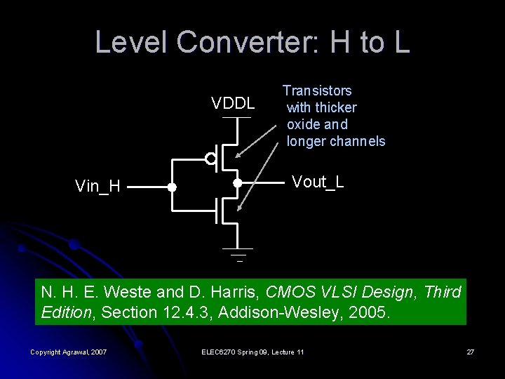
Level Converter: H to L VDDL Vin_H Transistors with thicker oxide and longer channels Vout_L N. H. E. Weste and D. Harris, CMOS VLSI Design, Third Edition, Section 12. 4. 3, Addison-Wesley, 2005. Copyright Agrawal, 2007 ELEC 6270 Spring 09, Lecture 11 27

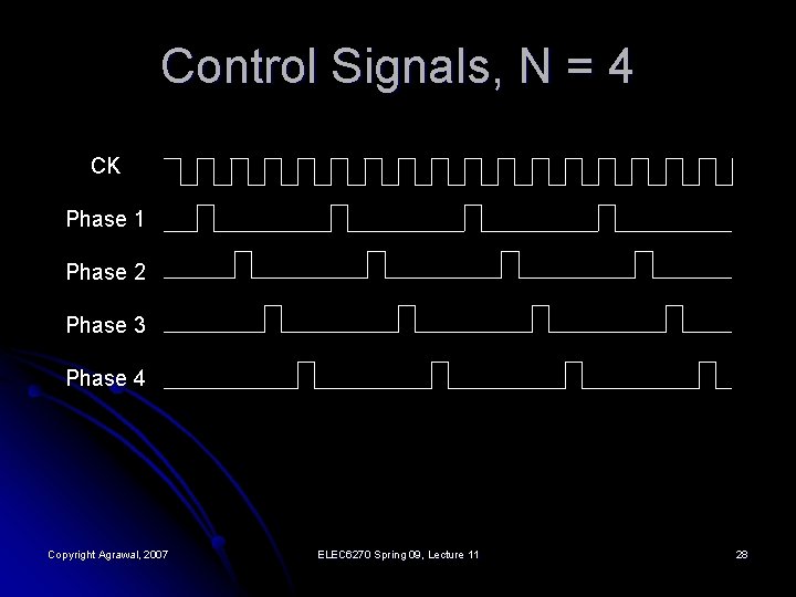
Control Signals, N = 4 CK Phase 1 Phase 2 Phase 3 Phase 4 Copyright Agrawal, 2007 ELEC 6270 Spring 09, Lecture 11 28

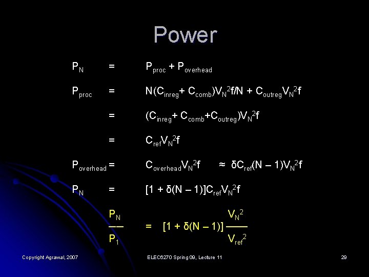
Power PN = Pproc + Poverhead Pproc = N(Cinreg+ Ccomb)VN 2 f/N + Coutreg. VN 2 f = (Cinreg+ Ccomb+Coutreg)VN 2 f = Cref. VN 2 f Poverhead = Coverhead. VN 2 f PN [1 + δ(N – 1)]Cref. VN 2 f = PN ── P 1 Copyright Agrawal, 2007 = ≈ δCref(N – 1)VN 2 f VN 2 [1 + δ(N – 1)] ─── Vref 2 ELEC 6270 Spring 09, Lecture 11 29

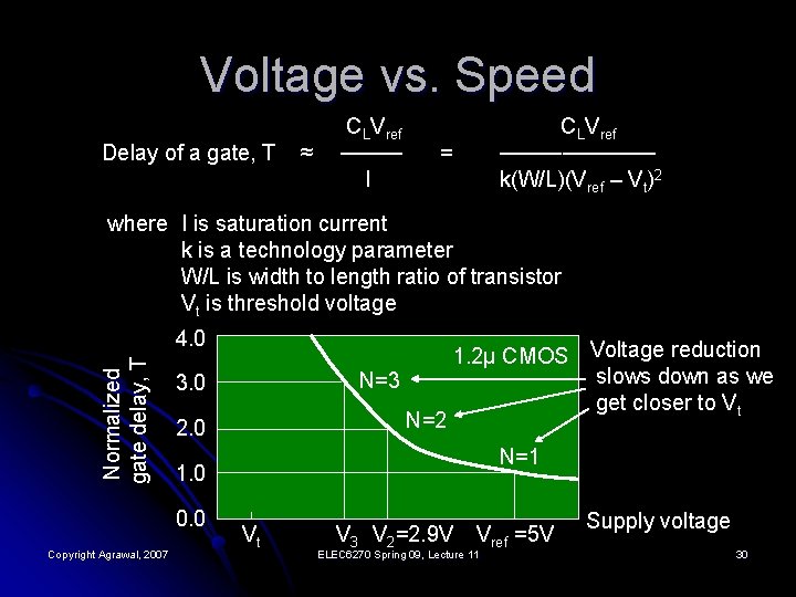
Voltage vs. Speed Delay of a gate, T ≈ CLVref ──── I CLVref ───── k(W/L)(Vref – Vt)2 = where I is saturation current k is a technology parameter W/L is width to length ratio of transistor Vt is threshold voltage Normalized gate delay, T 4. 0 N=2 2. 0 N=1 1. 0 0. 0 Copyright Agrawal, 2007 N=3 3. 0 1. 2μ CMOS Voltage reduction slows down as we get closer to Vt Vt V 3 V 2=2. 9 V Vref =5 V ELEC 6270 Spring 09, Lecture 11 Supply voltage 30

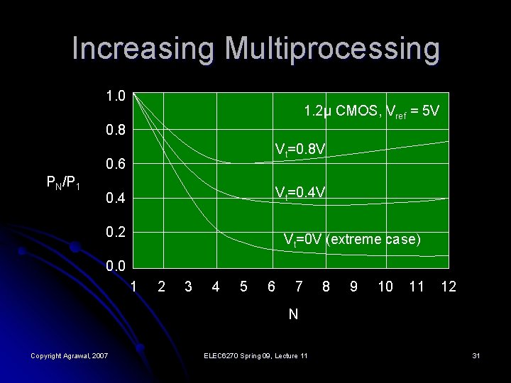
Increasing Multiprocessing 1. 0 1. 2μ CMOS, Vref = 5 V 0. 8 Vt=0. 8 V 0. 6 PN/P 1 Vt=0. 4 V 0. 4 0. 2 Vt=0 V (extreme case) 0. 0 1 2 3 4 5 6 7 8 9 10 11 12 N Copyright Agrawal, 2007 ELEC 6270 Spring 09, Lecture 11 31

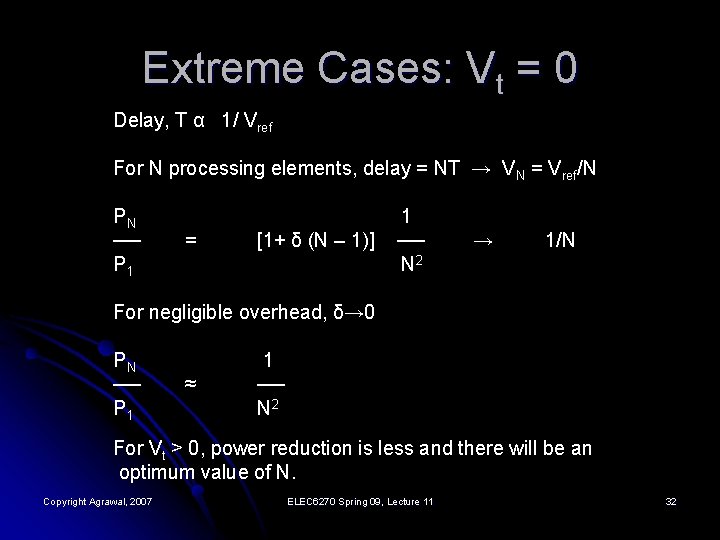
Extreme Cases: Vt = 0 Delay, T α 1/ Vref For N processing elements, delay = NT → VN = Vref/N PN ── P 1 = [1+ δ (N – 1)] 1 ── N 2 → 1/N For negligible overhead, δ→ 0 PN ── P 1 ≈ 1 ── N 2 For Vt > 0, power reduction is less and there will be an optimum value of N. Copyright Agrawal, 2007 ELEC 6270 Spring 09, Lecture 11 32

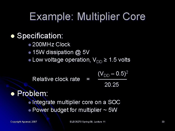
Example: Multiplier Core l Specification: l 200 MHz Clock l 15 W dissipation @ 5 V l Low voltage operation, VDD ≥ 1. 5 volts Relative clock rate l = (VDD – 0. 5)2 ─────── 20. 25 Problem: l Integrate multiplier core on a SOC l Power budget for multiplier ~ 5 W Copyright Agrawal, 2007 ELEC 6270 Spring 09, Lecture 11 33

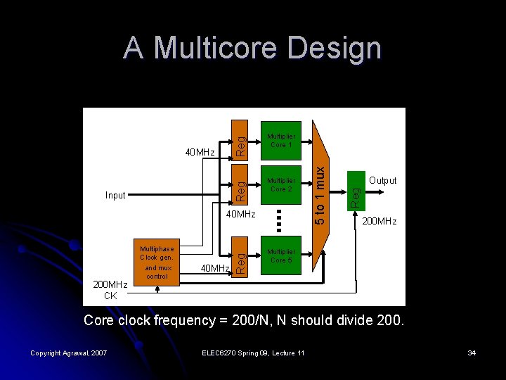
Input Multiplier Core 2 200 MHz CK Multiphase Clock gen. and mux control 40 MHz Reg 40 MHz Output Reg 40 MHz Multiplier Core 1 5 to 1 mux Reg A Multicore Design 200 MHz Multiplier Core 5 Core clock frequency = 200/N, N should divide 200. Copyright Agrawal, 2007 ELEC 6270 Spring 09, Lecture 11 34

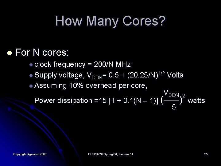
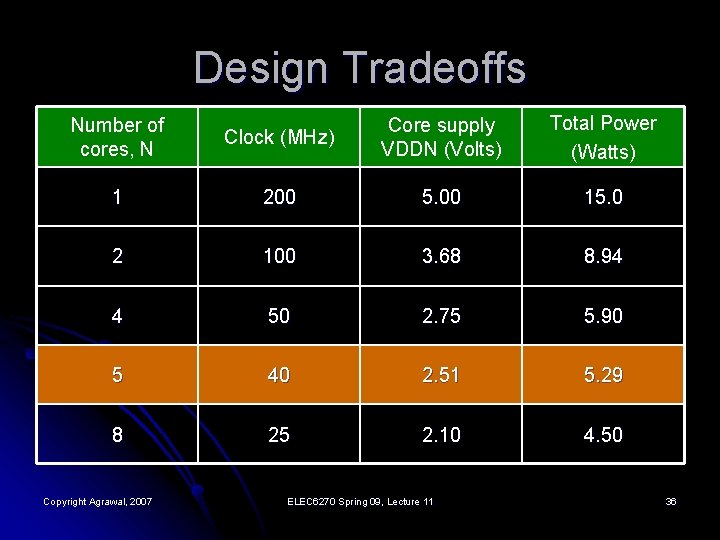
How Many Cores? l For N cores: l clock frequency = 200/N MHz l Supply voltage, VDDN= 0. 5 + (20. 25/N)1/2 Volts l Assuming 10% overhead per core, VDDN 2 Power dissipation =15 [1 + 0. 1(N – 1)] (───) watts 5 Copyright Agrawal, 2007 ELEC 6270 Spring 09, Lecture 11 35

Design Tradeoffs Clock (MHz) Core supply VDDN (Volts) Total Power (Watts) 1 200 5. 00 15. 0 2 100 3. 68 8. 94 4 50 2. 75 5. 90 5 40 2. 51 5. 29 8 25 2. 10 4. 50 Number of cores, N Copyright Agrawal, 2007 ELEC 6270 Spring 09, Lecture 11 36

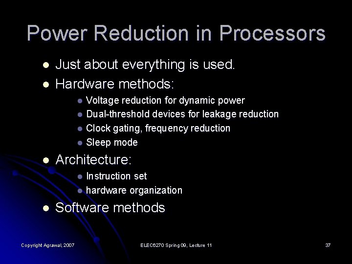
Power Reduction in Processors l l Just about everything is used. Hardware methods: Voltage reduction for dynamic power l Dual-threshold devices for leakage reduction l Clock gating, frequency reduction l Sleep mode l l Architecture: Instruction set l hardware organization l l Software methods Copyright Agrawal, 2007 ELEC 6270 Spring 09, Lecture 11 37

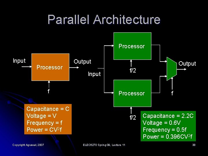
Parallel Architecture Processor Input Processor Output f/2 Input f Processor Capacitance = C Voltage = V Frequency = f Power = CV 2 f f/2 Copyright Agrawal, 2007 ELEC 6270 Spring 09, Lecture 11 f Capacitance = 2. 2 C Voltage = 0. 6 V Frequency = 0. 5 f Power = 0. 396 CV 2 f 38

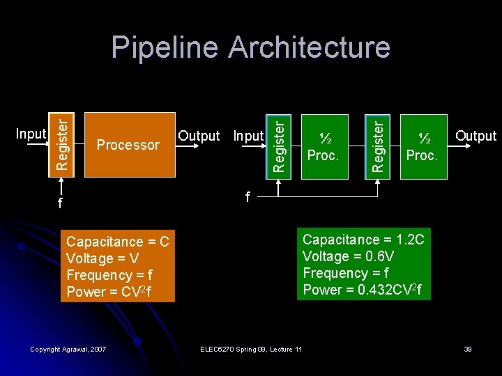
Output Input ½ Proc. Register Processor Register Input Register Pipeline Architecture ½ Proc. Output f f Capacitance = C Voltage = V Frequency = f Power = CV 2 f Copyright Agrawal, 2007 Capacitance = 1. 2 C Voltage = 0. 6 V Frequency = f Power = 0. 432 CV 2 f ELEC 6270 Spring 09, Lecture 11 39

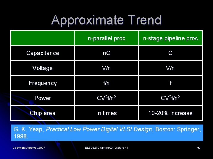
Approximate Trend n-parallel proc. n-stage pipeline proc. Capacitance n. C C Voltage V/n Frequency f/n f Power CV 2 f/n 2 Chip area n times 10 -20% increase G. K. Yeap, Practical Low Power Digital VLSI Design, Boston: Springer, 1998. Copyright Agrawal, 2007 ELEC 6270 Spring 09, Lecture 11 40

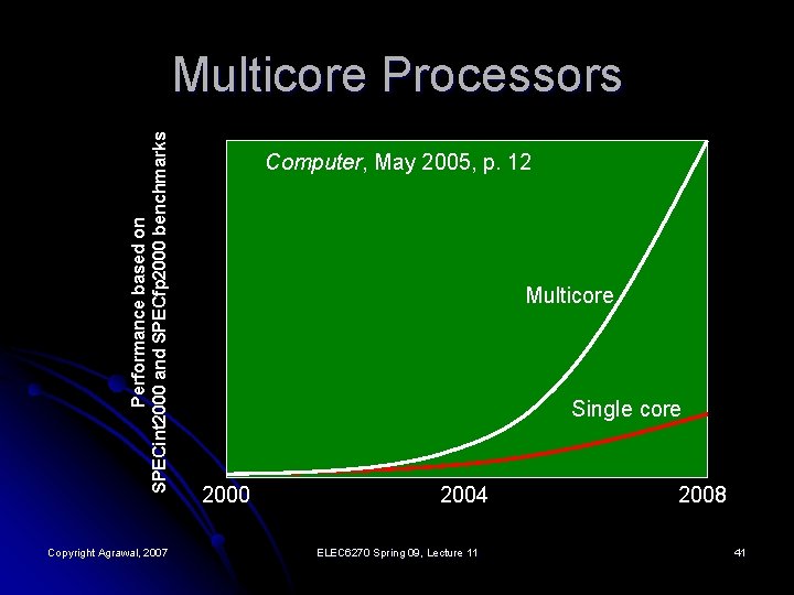
Performance based on SPECint 2000 and SPECfp 2000 benchmarks Multicore Processors Copyright Agrawal, 2007 Computer, May 2005, p. 12 Multicore Single core 2000 2004 ELEC 6270 Spring 09, Lecture 11 2008 41

Multicore Processors l l l D. Geer, “Chip Makers Turn to Multicore Processors, ” Computer, vol. 38, no. 5, pp. 11 -13, May 2005. A. Jerraya, H. Tenhunen and W. Wolf, “Multiprocessor Systems-on-Chips, ” Computer, vol. 5, no. 7, pp. 36 -40, July 2005; this special issue contains three more articles on multicore processors. S. K. Moore, “Winner Multimedia Monster – Cell’s Nine Processors Make It a Supercomputer on a Chip, ” IEEE Spectrum, vol. 43. no. 1, pp. 20 -23, January 2006. Copyright Agrawal, 2007 ELEC 6270 Spring 09, Lecture 11 42

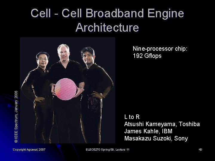
Cell - Cell Broadband Engine Architecture © IEEE Spectrum, January 2006 Nine-processor chip: 192 Gflops Copyright Agrawal, 2007 L to R Atsushi Kameyama, Toshiba James Kahle, IBM Masakazu Suzoki, Sony ELEC 6270 Spring 09, Lecture 11 43

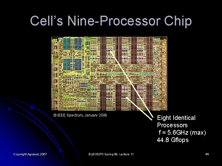
Cell’s Nine-Processor Chip © IEEE Spectrum, January 2006 Copyright Agrawal, 2007 ELEC 6270 Spring 09, Lecture 11 Eight Identical Processors f = 5. 6 GHz (max) 44. 8 Gflops 44