ELEC 52706270 Spring 2015 LowPower Design of Electronic


- Slides: 40

ELEC 5270/6270 Spring 2015 Low-Power Design of Electronic Circuits Pass Transistor Logic: A Low Power Logic Family Vishwani D. Agrawal James J. Danaher Professor Dept. of Electrical and Computer Engineering Auburn University, Auburn, AL 36849 vagrawal@eng. auburn. edu http: //www. eng. auburn. edu/~vagrawal/COURSE/E 6270_Spr 15/course. html Copyright Agrawal, 2007 ELEC 6270 Spring 15, Lecture 12 1

Low-Power Logic Styles Pass transistor logic l Dynamic logic l Domino logic l Adiabatic and charge recovery logic l Asynchronous logic l Logic restructuring l Copyright Agrawal, 2007 ELEC 6270 Spring 15, Lecture 12 2

Pass Transistor Logic (PTL) l Requires fewer transistors l Smaller area l Reduced capacitance l Reduced energy and power Copyright Agrawal, 2007 ELEC 6270 Spring 15, Lecture 12 3

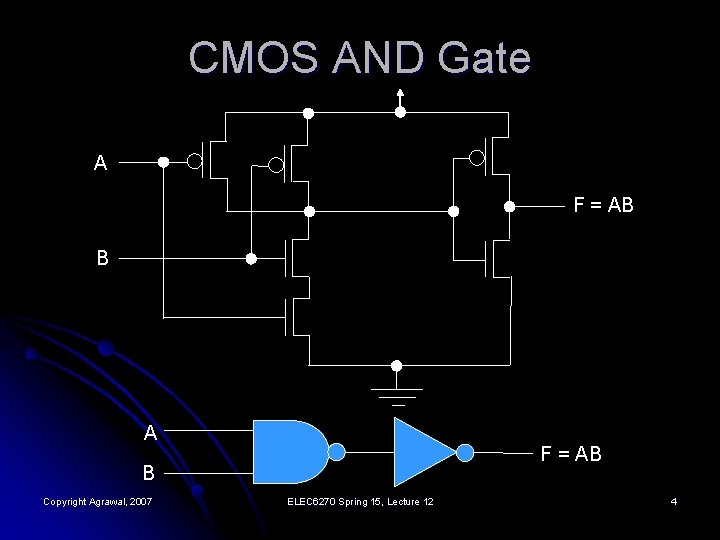
CMOS AND Gate A F = AB B Copyright Agrawal, 2007 ELEC 6270 Spring 15, Lecture 12 4

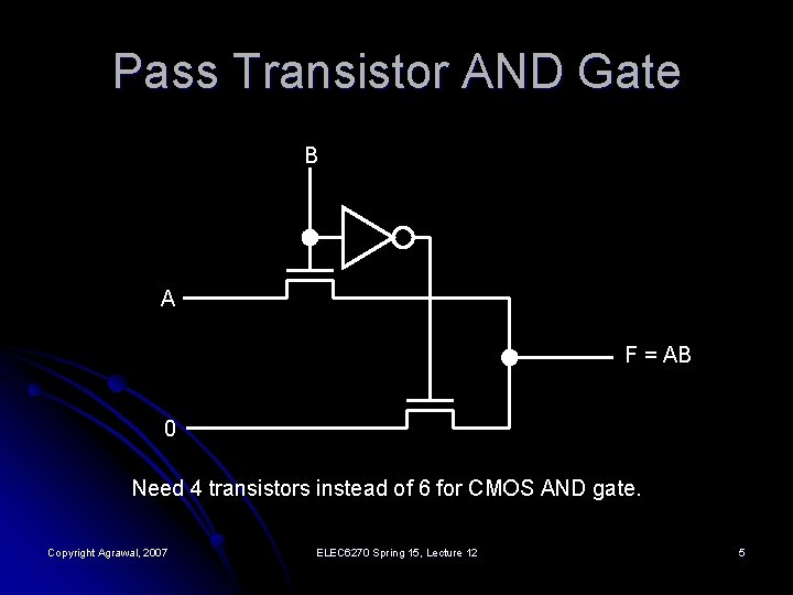
Pass Transistor AND Gate B A F = AB 0 Need 4 transistors instead of 6 for CMOS AND gate. Copyright Agrawal, 2007 ELEC 6270 Spring 15, Lecture 12 5

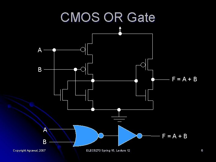
CMOS OR Gate A B F=A+B A F=A+B B Copyright Agrawal, 2007 ELEC 6270 Spring 15, Lecture 12 6

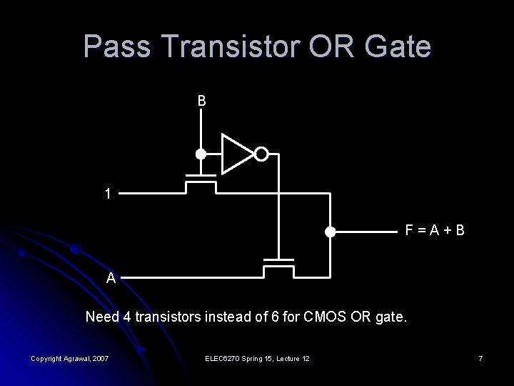
Pass Transistor OR Gate B 1 F=A+B A Need 4 transistors instead of 6 for CMOS OR gate. Copyright Agrawal, 2007 ELEC 6270 Spring 15, Lecture 12 7

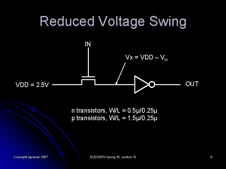
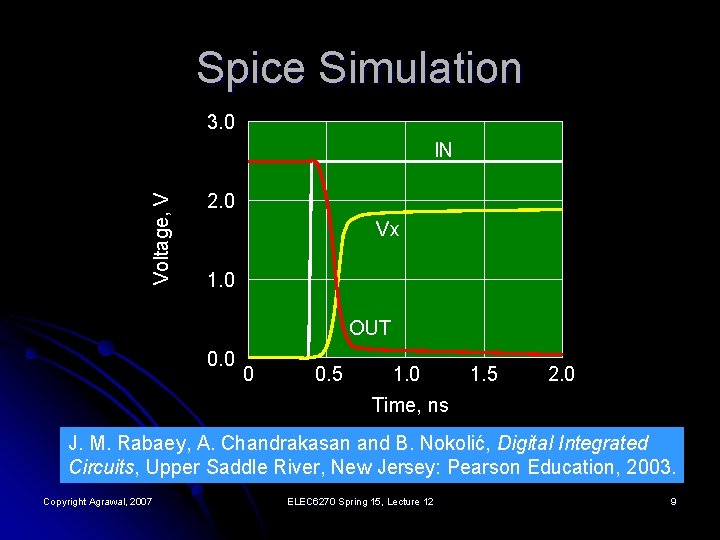
Reduced Voltage Swing IN Vx = VDD – Vtn OUT VDD = 2. 5 V n transistors, W/L = 0. 5μ/0. 25μ p transistors, W/L = 1. 5μ/0. 25μ Copyright Agrawal, 2007 ELEC 6270 Spring 15, Lecture 12 8

Spice Simulation 3. 0 Voltage, V IN 2. 0 Vx 1. 0 OUT 0. 0 0 0. 5 1. 0 1. 5 2. 0 Time, ns J. M. Rabaey, A. Chandrakasan and B. Nokolić, Digital Integrated Circuits, Upper Saddle River, New Jersey: Pearson Education, 2003. Copyright Agrawal, 2007 ELEC 6270 Spring 15, Lecture 12 9

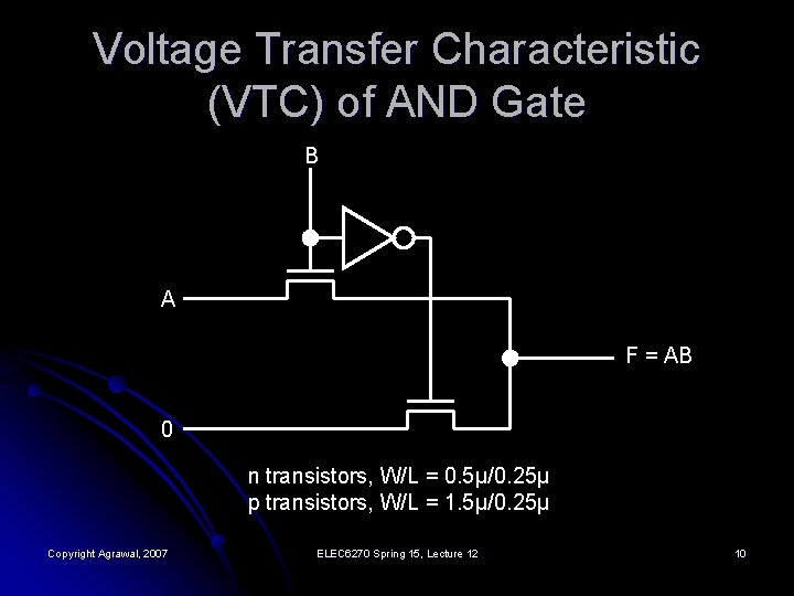
Voltage Transfer Characteristic (VTC) of AND Gate B A F = AB 0 n transistors, W/L = 0. 5μ/0. 25μ p transistors, W/L = 1. 5μ/0. 25μ Copyright Agrawal, 2007 ELEC 6270 Spring 15, Lecture 12 10

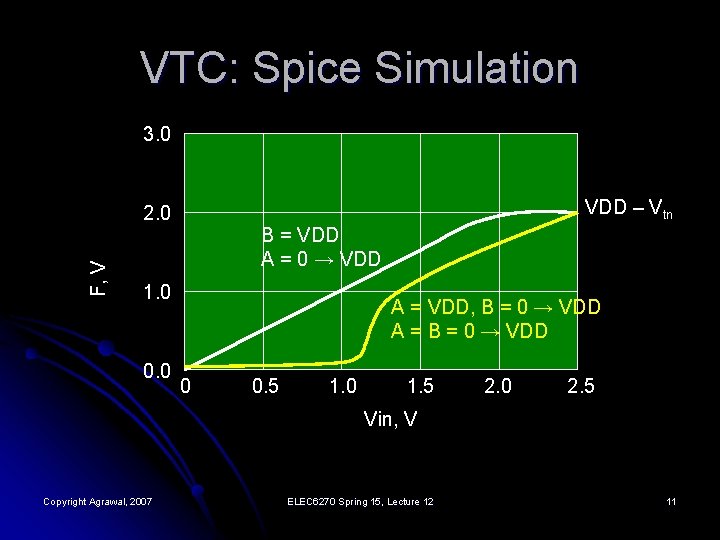
VTC: Spice Simulation 3. 0 VDD – Vtn F, V 2. 0 B = VDD A = 0 → VDD 1. 0 0. 0 A = VDD, B = 0 → VDD A = B = 0 → VDD 0 0. 5 1. 0 1. 5 2. 0 2. 5 Vin, V Copyright Agrawal, 2007 ELEC 6270 Spring 15, Lecture 12 11

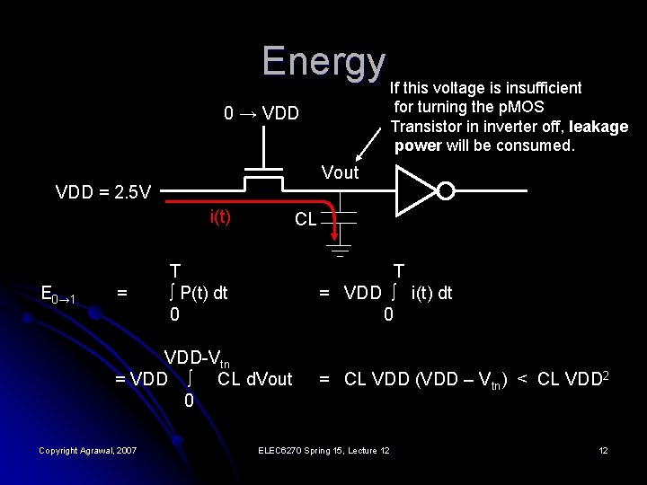
Energy If this voltage is insufficient for turning the p. MOS Transistor in inverter off, leakage power will be consumed. 0 → VDD Vout VDD = 2. 5 V i(t) E 0→ 1 = CL T ∫ P(t) dt 0 T = VDD ∫ i(t) dt 0 VDD-Vtn = VDD ∫ CL d. Vout 0 Copyright Agrawal, 2007 = CL VDD (VDD – Vtn) < CL VDD 2 ELEC 6270 Spring 15, Lecture 12 12

Energy: PTL vs. CMOS PTL consumes less dynamic power than static CMOS Logic. l PTL leakage may be higher when inverter output is low, because the reduced voltage level may be insufficient to turn the PMOS transistor in the inverter off. l Copyright Agrawal, 2007 ELEC 6270 Spring 15, Lecture 12 13

Ways to Reduce Leakage Level restoration l Multiple-threshold transistors l Transmission-gate logic l Copyright Agrawal, 2007 ELEC 6270 Spring 15, Lecture 12 14

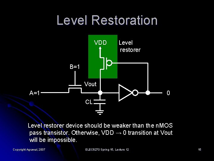
Level Restoration VDD Level restorer B=1 Vout A=1 0 CL Level restorer device should be weaker than the n. MOS pass transistor. Otherwise, VDD → 0 transition at Vout will be impossible. Copyright Agrawal, 2007 ELEC 6270 Spring 15, Lecture 12 15

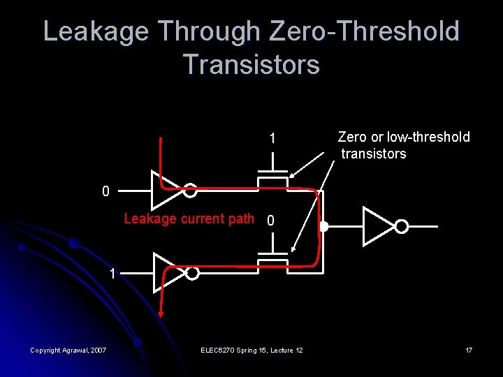
Multiple-Threshold Transistors Use zero-threshold pass-transistors. l Use high-threshold transistors in all other gates. l This can cause leakage through multiple gates. l Copyright Agrawal, 2007 ELEC 6270 Spring 15, Lecture 12 16

Leakage Through Zero-Threshold Transistors 1 Zero or low-threshold transistors 0 Leakage current path 0 1 Copyright Agrawal, 2007 ELEC 6270 Spring 15, Lecture 12 17

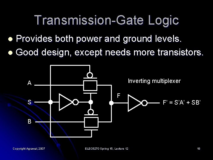
Transmission-Gate Logic Provides both power and ground levels. l Good design, except needs more transistors. l Inverting multiplexer A S F F’ = S’A’ + SB’ B Copyright Agrawal, 2007 ELEC 6270 Spring 15, Lecture 12 18

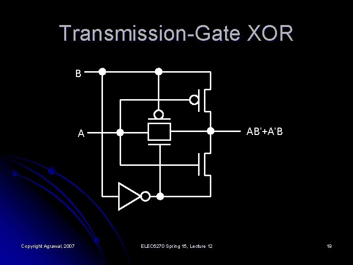
Transmission-Gate XOR B AB’+A’B A Copyright Agrawal, 2007 ELEC 6270 Spring 15, Lecture 12 19

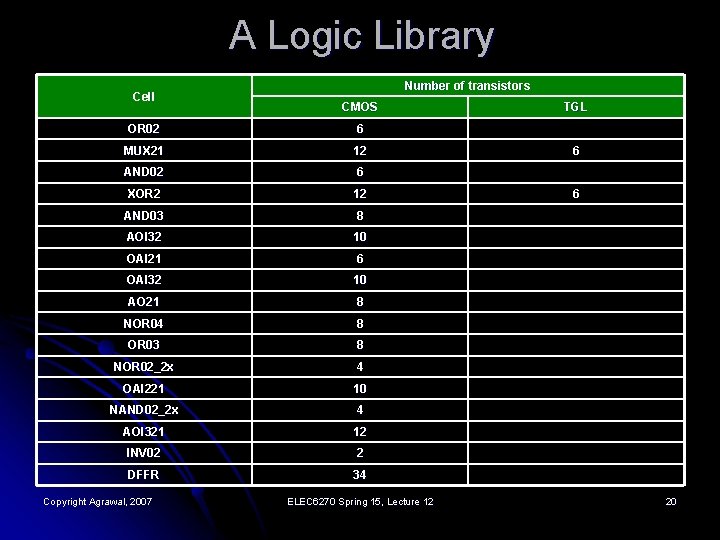
A Logic Library Cell Number of transistors CMOS OR 02 6 MUX 21 12 AND 02 6 XOR 2 12 AND 03 8 AOI 32 10 OAI 21 6 OAI 32 10 AO 21 8 NOR 04 8 OR 03 8 NOR 02_2 x 4 OAI 221 10 NAND 02_2 x 4 AOI 321 12 INV 02 2 DFFR 34 Copyright Agrawal, 2007 ELEC 6270 Spring 15, Lecture 12 TGL 6 6 20

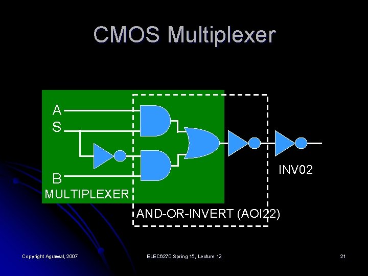
CMOS Multiplexer A S INV 02 B MULTIPLEXER AND-OR-INVERT (AOI 22) Copyright Agrawal, 2007 ELEC 6270 Spring 15, Lecture 12 21

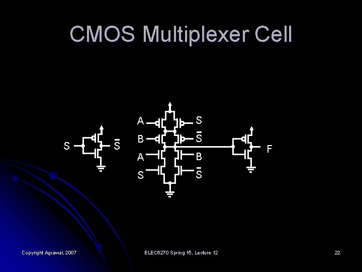
CMOS Multiplexer Cell S Copyright Agrawal, 2007 S A S B S A B S S ELEC 6270 Spring 15, Lecture 12 F 22

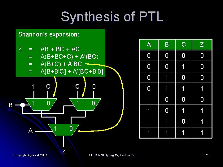
Synthesis of PTL Shannon’s expansion: Z B = = AB + BC + AC A(B+BC+C) + A’(BC) A(B+C) + A’BC A[B+B’C] + A’[BC+B’ 0] 1 C C 0 1 0 A Copyright Agrawal, 2007 1 0 Z ELEC 6270 Spring 15, Lecture 12 A B C Z 0 0 0 1 1 0 0 0 1 1 1 1 0 1 1 1 23

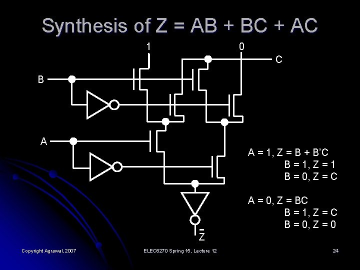
Synthesis of Z = AB + BC + AC 0 1 C B A A = 1, Z = B + B’C B = 1, Z = 1 B = 0, Z = C A = 0, Z = BC B = 1, Z = C B = 0, Z = 0 Z Copyright Agrawal, 2007 ELEC 6270 Spring 15, Lecture 12 24

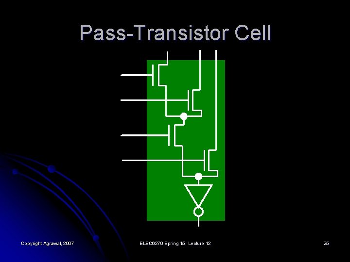
Pass-Transistor Cell Copyright Agrawal, 2007 ELEC 6270 Spring 15, Lecture 12 25

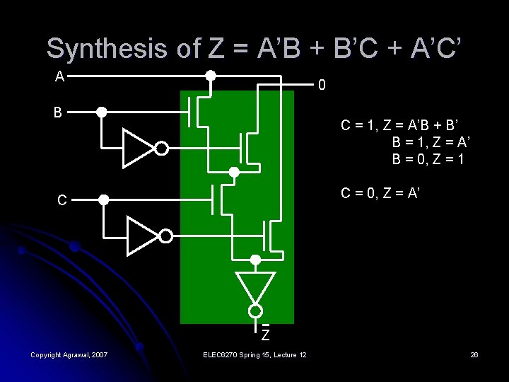
Synthesis of Z = A’B + B’C + A’C’ A 0 B C = 1, Z = A’B + B’ B = 1, Z = A’ B = 0, Z = 1 C = 0, Z = A’ C Z Copyright Agrawal, 2007 ELEC 6270 Spring 15, Lecture 12 26

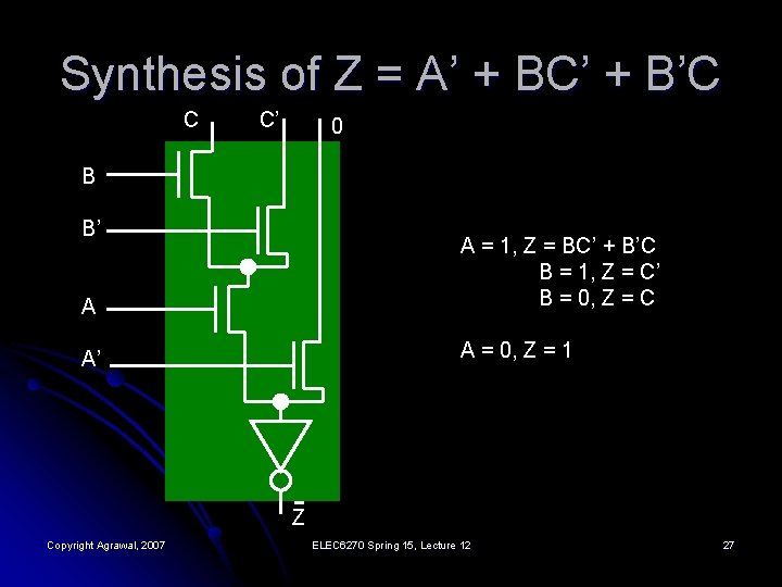
Synthesis of Z = A’ + BC’ + B’C C C’ 0 B B’ A A = 1, Z = BC’ + B’C B = 1, Z = C’ B = 0, Z = C A’ A = 0, Z = 1 Z Copyright Agrawal, 2007 ELEC 6270 Spring 15, Lecture 12 27

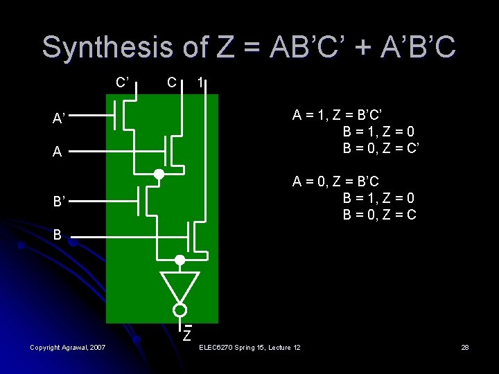
Synthesis of Z = AB’C’ + A’B’C C’ C 1 A = 1, Z = B’C’ B = 1, Z = 0 B = 0, Z = C’ A’ A A = 0, Z = B’C B = 1, Z = 0 B = 0, Z = C B’ B Z Copyright Agrawal, 2007 ELEC 6270 Spring 15, Lecture 12 28

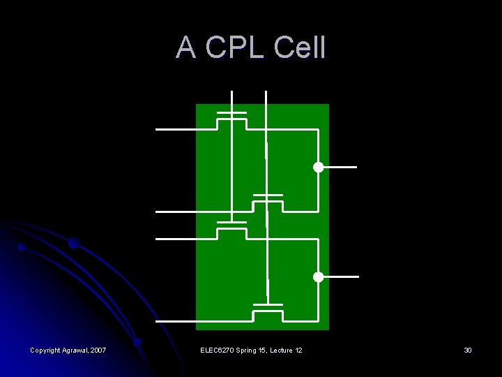
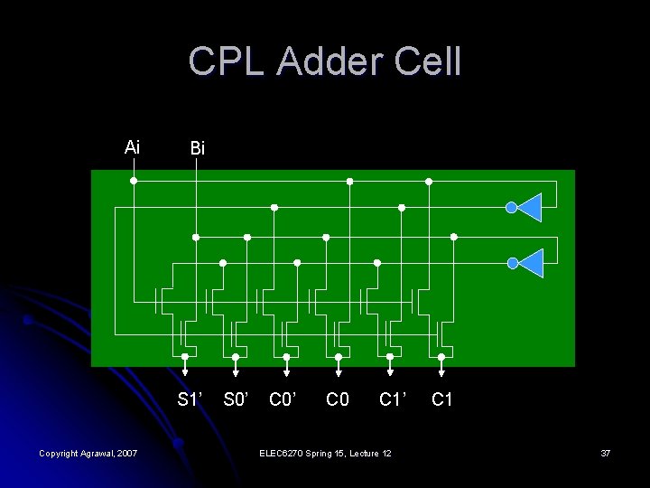
CPL: Complementary Pass. Transistor Logic Every signal and its complement is generated. l Gates are static, because the output is connected to either VDD or GND. l Design is modular; same cell can produce various gates by simply permuting the input signals. l Also called differential pass-transistor logic (DPL) l Copyright Agrawal, 2007 ELEC 6270 Spring 15, Lecture 12 29

A CPL Cell Copyright Agrawal, 2007 ELEC 6270 Spring 15, Lecture 12 30

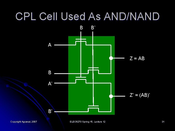
CPL Cell Used As AND/NAND B B’ A Z = AB B A’ Z’ = (AB)’ B’ Copyright Agrawal, 2007 ELEC 6270 Spring 15, Lecture 12 31

CPL Cell Used As OR/NOR B’ B A Z=A+B B A’ Z’ = (A + B)’ B’ Copyright Agrawal, 2007 ELEC 6270 Spring 15, Lecture 12 32

CPL Cell Used As XOR/XNOR B’ B A Z = AB’ + A’B A’ A’ Z’ = AB + A’B’ A Copyright Agrawal, 2007 ELEC 6270 Spring 15, Lecture 12 33

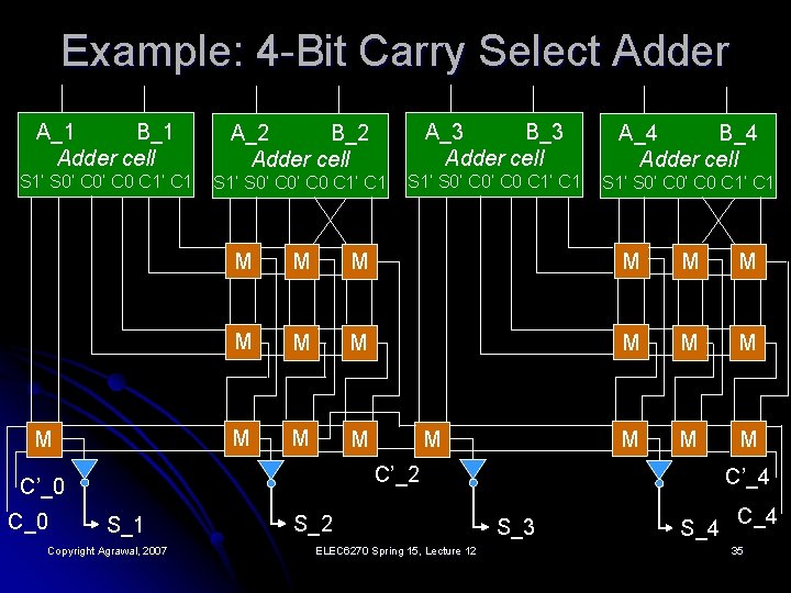
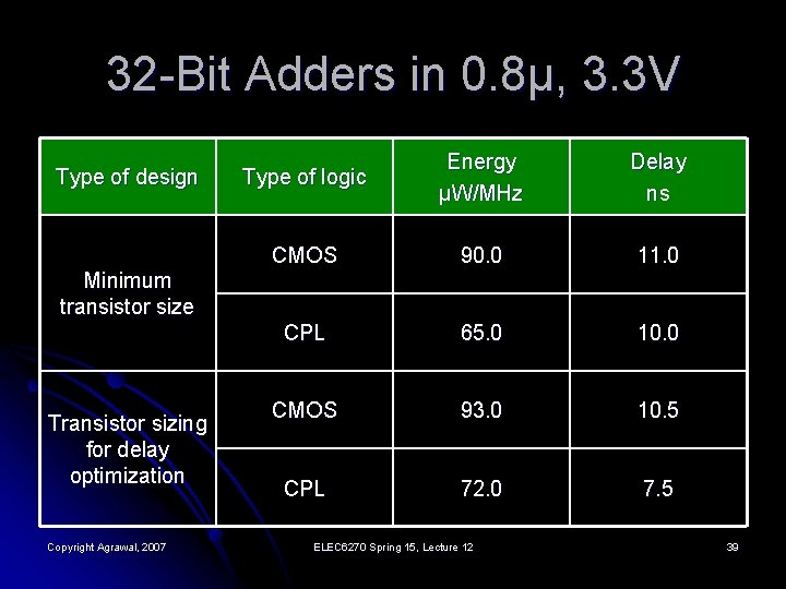
CPL vs. CMOS CPL requires fewer transistors. l Useful for modular (array) circuits like adders, multipliers, barrel shifter, etc. l CPL operation can be faster and energy efficient. l Following example is taken from: l l M. E. Elrabaa, I. S. Abu-Khater, and M. I. Elmasry, Advanced Low-Power Digital Circuit Techniques, Springer, 1997, Chapter 2. Copyright Agrawal, 2007 ELEC 6270 Spring 15, Lecture 12 34

Example: 4 -Bit Carry Select Adder A_1 B_1 Adder cell A_2 B_2 Adder cell A_3 B_3 Adder cell A_4 B_4 Adder cell S 1’ S 0’ C 0’ C 0 C 1’ C 1 M M M M M C’_2 C’_0 C_0 M S_1 Copyright Agrawal, 2007 S_2 ELEC 6270 Spring 15, Lecture 12 C’_4 S_3 S_4 C_4 35

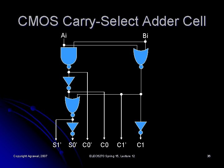
CMOS Carry-Select Adder Cell Ai S 1’ Copyright Agrawal, 2007 Bi S 0’ C 0 C 1’ ELEC 6270 Spring 15, Lecture 12 C 1 36

CPL Adder Cell Ai Bi S 1’ Copyright Agrawal, 2007 S 0’ C 0 C 1’ ELEC 6270 Spring 15, Lecture 12 C 1 37

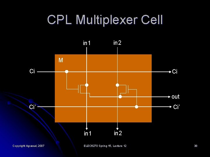
CPL Multiplexer Cell in 1 in 2 M Ci Ci out Ci’ in 1 Copyright Agrawal, 2007 in 2 ELEC 6270 Spring 15, Lecture 12 38

32 -Bit Adders in 0. 8μ, 3. 3 V Type of design Type of logic Energy μW/MHz Delay ns CMOS 90. 0 11. 0 CPL 65. 0 10. 0 CMOS 93. 0 10. 5 CPL 72. 0 7. 5 Minimum transistor size Transistor sizing for delay optimization Copyright Agrawal, 2007 ELEC 6270 Spring 15, Lecture 12 39

References G. R. Cho and T. Chen, “On the Impact of Technology Scaling on Mixed PTL/Static Logic, ” Proc. IEEE Int. Conf. Computer Design, 2002, pp. 322 -326. l R. Zimmermann and W. Fichtner, “Low. Power Logic Styles: CMOS Versus Pass. Transistor Logic, ” IEEE J. Solid State Circuits, vol. 32, no. 7, pp. 1079 -1090, July 1997. l Copyright Agrawal, 2007 ELEC 6270 Spring 15, Lecture 12 40