ELEC 52706270 Spring 2009 LowPower Design of Electronic

![Example: maxtran With Non-Zero k [n 1 = 6] EAsv = - ∞ EAdv Example: maxtran With Non-Zero k [n 1 = 6] EAsv = - ∞ EAdv](https://slidetodoc.com/presentation_image_h/a9ae943a8cc846f88c7fb02398b03916/image-19.jpg)
- Slides: 34

ELEC 5270/6270 Spring 2009 Low-Power Design of Electronic Circuits Power Analysis and Process Variation Vishwani D. Agrawal James J. Danaher Professor Dept. of Electrical and Computer Engineering Auburn University, Auburn, AL 36849 vagrawal@eng. auburn. edu http: //www. eng. auburn. edu/~vagrawal/COURSE/E 6270_Spr 09/course. html Copyright Agrawal, 2009 ELEC 5270 -001/6270 -001 Spr 09, Lecture 6 1

Process Variation in Nanoscale Devices l l l Nanoscale device have dimensions smaller than 100 nm, typically, 65 nm, 45 nm, 32 nm, 22 nm, etc. As geometries become closer to molecular dimensions, percentage random variation in parameters become large. Affected physical parameters: transistor width (W) and length (L), interconnect width and spacing, doping level. Affected electrical characteristics: on and off resistances of transistors, threshold voltage and leakage current, capacitances. Major influence on gate delays, ± 20%, or more. Copyright Agrawal, 2009 ELEC 5270 -001/6270 -001 Spr 09, Lecture 6 2

Dynamic Power and Process Variation Dynamic power increases with glitch transitions, which are functions of gate delays. l Process variation can influence delays in a circuit, especially in nanoscale technologies. l Monte Carlo simulation used to address the variation is time consuming and expensive. l Bounded delay models are usually considered to address process variations in logic level simulation and timing analysis. l Copyright Agrawal, 2009 ELEC 5270 -001/6270 -001 Spr 09, Lecture 6 3

l l l References Simulation: l S. Chakraborty and D. L. Dill, “More Accurate Polynomial-Time Min. Max Timing Simulation, ” Proc. 3 rd International Symp. Advanced Research in Asynchronous Cir. and Syst. , Apr. 1997, pp. 112 -123. l J. W. Bierbauer, J. A. Eiseman, F. A. Fazal, and J. J. Kulikowski, “System Simulation With MIDAS, ” AT&T Tech. J. , vol. 70, no. 1, pp. 36– 51, Jan. 1991. l S. Bose, H. Grimes, and V. D. Agrawal, “Delay Fault Simulation With Bounded Gate Delay Model, ” Proc. International Test Conf. , 2007, pp. 23– 28. Timing anlysis: l S. Chakraborty, D. L. Dill, and K. Y. Yun, “Min-Max Timing Analysis and an Application to Asynchronous Circuits, ” Proc. IEEE, vol. 87, no. 2, pp. 332– 346, Feb. 1999. Delay fault testing: l H. Grimes, Reconvergent Fanout Analysis of Bounded Gate Delay Faults, Master’s thesis, Auburn University, Dept. of ECE, Aug. 2008. Copyright Agrawal, 2009 ELEC 5270 -001/6270 -001 Spr 09, Lecture 6 4

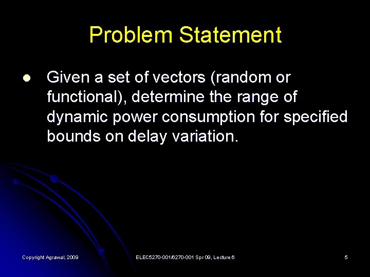
Problem Statement l Given a set of vectors (random or functional), determine the range of dynamic power consumption for specified bounds on delay variation. Copyright Agrawal, 2009 ELEC 5270 -001/6270 -001 Spr 09, Lecture 6 5

Power Analysis Methods l Monte Carlo simulation: l R. Burch, F. Najm, P. Yang, and T. Trick, “Mc. POWER: A Monte Carlo Approach to Power Estimation, ” Proc. IEEE/ACM International Conference on Computer-Aided Design, pp. 90– 97, Nov 1992. l Bounded-delay analysis: l J. D. Alexander, Simulation Based Power Estimation for Digital CMOS Technologies, Master’s thesis, Auburn University, Dept. of ECE, Dec. 2008. Copyright Agrawal, 2009 ELEC 5270 -001/6270 -001 Spr 09, Lecture 6 6

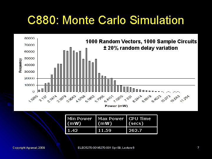
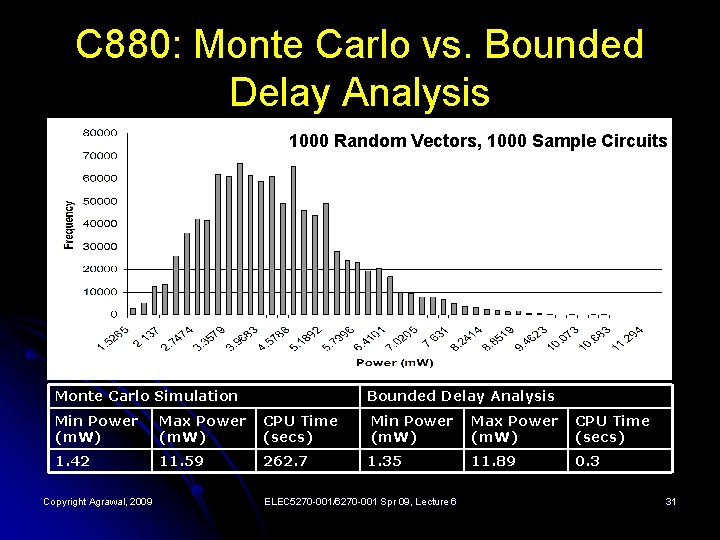
C 880: Monte Carlo Simulation 1000 Random Vectors, 1000 Sample Circuits ± 20% random delay variation Copyright Agrawal, 2009 Min Power (m. W) Max Power (m. W) CPU Time (secs) 1. 42 11. 59 262. 7 ELEC 5270 -001/6270 -001 Spr 09, Lecture 6 7

Bounded Delay Model delay uncertainties by assigning each gate a lower and an upper bound on delay, also known as min-max delay. l The bounds can be obtained by adding specified process-related variation to the nominal gate delay for the technology. l In this model, intervals of signal uncertainties are defined at the output of each gate. l Copyright Agrawal, 2009 ELEC 5270 -001/6270 -001 Spr 09, Lecture 6 8

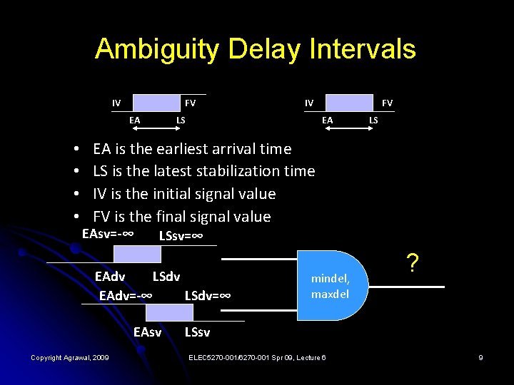
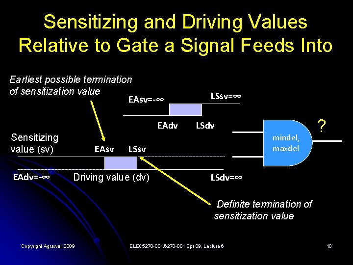
Ambiguity Delay Intervals IV FV EA • • IV LS FV EA LS EA is the earliest arrival time LS is the latest stabilization time IV is the initial signal value FV is the final signal value EAsv=-∞ LSsv=∞ EAdv LSdv EAdv=-∞ LSdv=∞ EAsv Copyright Agrawal, 2009 mindel, maxdel ? LSsv ELEC 5270 -001/6270 -001 Spr 09, Lecture 6 9

Sensitizing and Driving Values Relative to Gate a Signal Feeds Into Earliest possible termination of sensitization value EAsv=-∞ EAdv Sensitizing value (sv) EAdv=-∞ EAsv LSsv=∞ LSdv mindel, maxdel LSsv Driving value (dv) ? LSdv=∞ Definite termination of sensitization value Copyright Agrawal, 2009 ELEC 5270 -001/6270 -001 Spr 09, Lecture 6 10

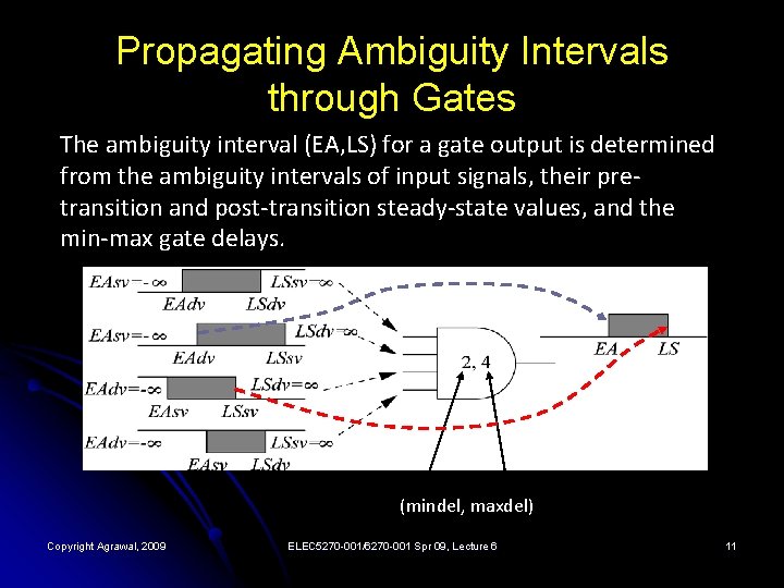
Propagating Ambiguity Intervals through Gates The ambiguity interval (EA, LS) for a gate output is determined from the ambiguity intervals of input signals, their pretransition and post-transition steady-state values, and the min-max gate delays. (mindel, maxdel) Copyright Agrawal, 2009 ELEC 5270 -001/6270 -001 Spr 09, Lecture 6 11

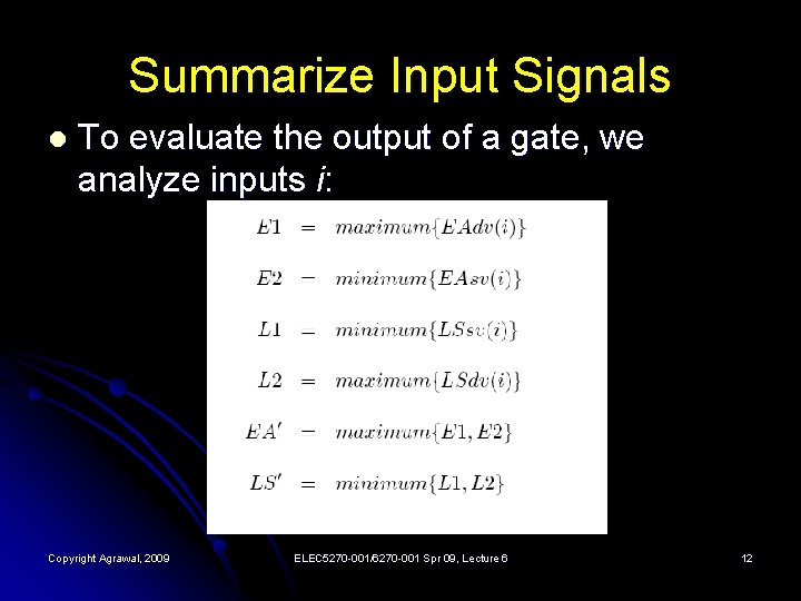
Summarize Input Signals l To evaluate the output of a gate, we analyze inputs i: Copyright Agrawal, 2009 ELEC 5270 -001/6270 -001 Spr 09, Lecture 6 12

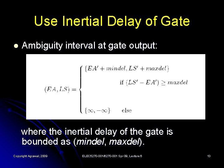
Use Inertial Delay of Gate l Ambiguity interval at gate output: where the inertial delay of the gate is bounded as (mindel, maxdel). Copyright Agrawal, 2009 ELEC 5270 -001/6270 -001 Spr 09, Lecture 6 13

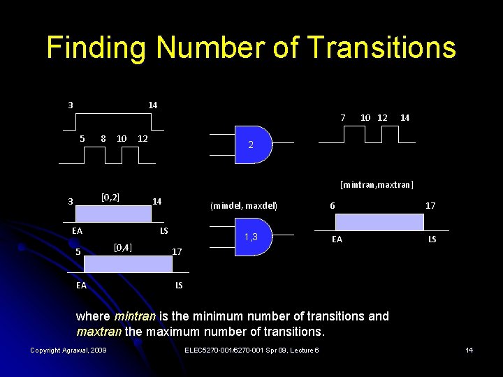
Finding Number of Transitions 3 14 7 5 8 10 12 14 2 [mintran, maxtran] [0, 2] 3 EA 5 EA 14 (mindel, maxdel) LS [0, 4] 1, 3 6 EA 17 LS where mintran is the minimum number of transitions and maxtran the maximum number of transitions. Copyright Agrawal, 2009 ELEC 5270 -001/6270 -001 Spr 09, Lecture 6 14

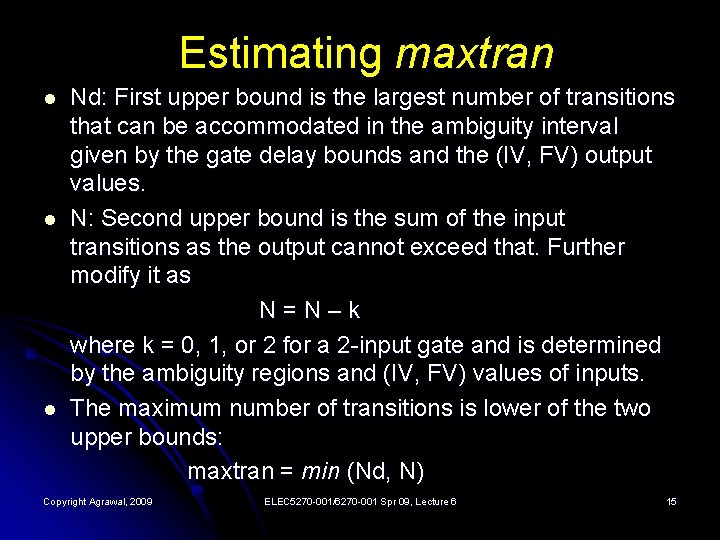
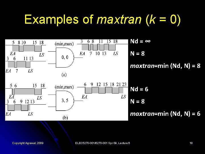
Estimating maxtran l l l Nd: First upper bound is the largest number of transitions that can be accommodated in the ambiguity interval given by the gate delay bounds and the (IV, FV) output values. N: Second upper bound is the sum of the input transitions as the output cannot exceed that. Further modify it as N=N–k where k = 0, 1, or 2 for a 2 -input gate and is determined by the ambiguity regions and (IV, FV) values of inputs. The maximum number of transitions is lower of the two upper bounds: maxtran = min (Nd, N) Copyright Agrawal, 2009 ELEC 5270 -001/6270 -001 Spr 09, Lecture 6 15

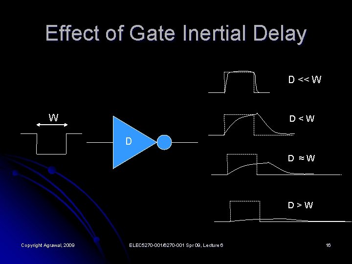
Effect of Gate Inertial Delay D << W W D<W D D ≈W D>W Copyright Agrawal, 2009 ELEC 5270 -001/6270 -001 Spr 09, Lecture 6 16

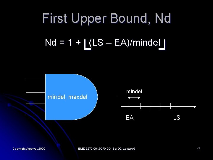
First Upper Bound, Nd Nd = 1 + (LS – EA)/mindel └ mindel, maxdel ┘ mindel EA Copyright Agrawal, 2009 ELEC 5270 -001/6270 -001 Spr 09, Lecture 6 LS 17

Examples of maxtran (k = 0) Nd = ∞ N=8 maxtran=min (Nd, N) = 8 Nd = 6 N=8 maxtran=min (Nd, N) = 6 Copyright Agrawal, 2009 ELEC 5270 -001/6270 -001 Spr 09, Lecture 6 18
![Example maxtran With NonZero k n 1 6 EAsv EAdv Example: maxtran With Non-Zero k [n 1 = 6] EAsv = - ∞ EAdv](https://slidetodoc.com/presentation_image_h/a9ae943a8cc846f88c7fb02398b03916/image-19.jpg)
Example: maxtran With Non-Zero k [n 1 = 6] EAsv = - ∞ EAdv EAsv = - ∞ LSdv = ∞ EA LSsv [n 2 = 4] EAdv [n 1 + n 2 – k = 8 ] , LS where k = 2 LSdv = ∞ LSsv [6] [6+4– 2=8] [4] Copyright Agrawal, 2009 ELEC 5270 -001/6270 -001 Spr 09, Lecture 6 19

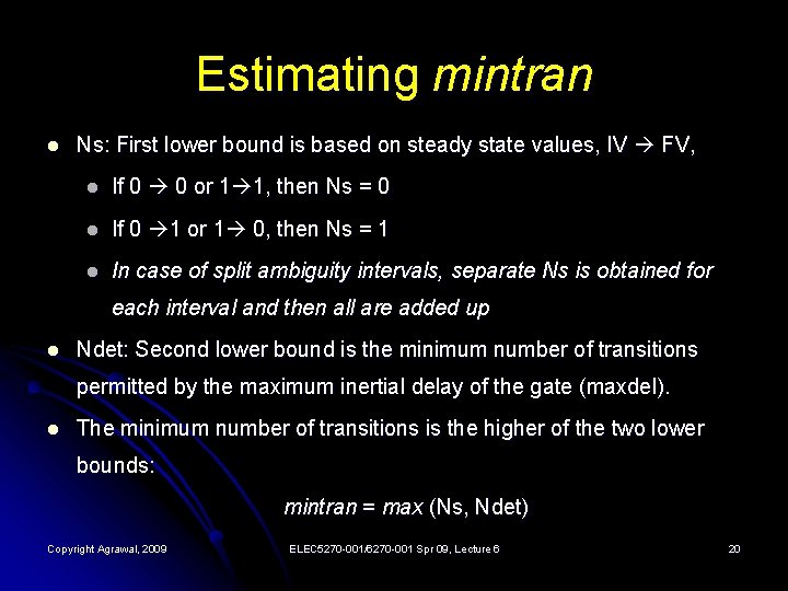
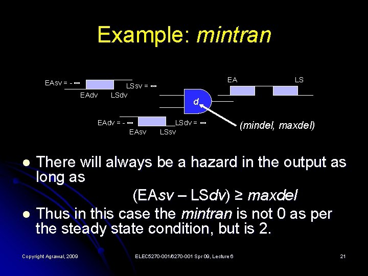
Estimating mintran l Ns: First lower bound is based on steady state values, IV FV, l If 0 0 or 1 1, then Ns = 0 l If 0 1 or 1 0, then Ns = 1 l In case of split ambiguity intervals, separate Ns is obtained for each interval and then all are added up l Ndet: Second lower bound is the minimum number of transitions permitted by the maximum inertial delay of the gate (maxdel). l The minimum number of transitions is the higher of the two lower bounds: mintran = max (Ns, Ndet) Copyright Agrawal, 2009 ELEC 5270 -001/6270 -001 Spr 09, Lecture 6 20

Example: mintran EAsv = - ∞ EAdv LSsv = ∞ LSdv EAdv = - ∞ EAsv EA LS d LSdv = ∞ LSsv (mindel, maxdel) There will always be a hazard in the output as long as (EAsv – LSdv) ≥ maxdel l Thus in this case the mintran is not 0 as per the steady state condition, but is 2. l Copyright Agrawal, 2009 ELEC 5270 -001/6270 -001 Spr 09, Lecture 6 21

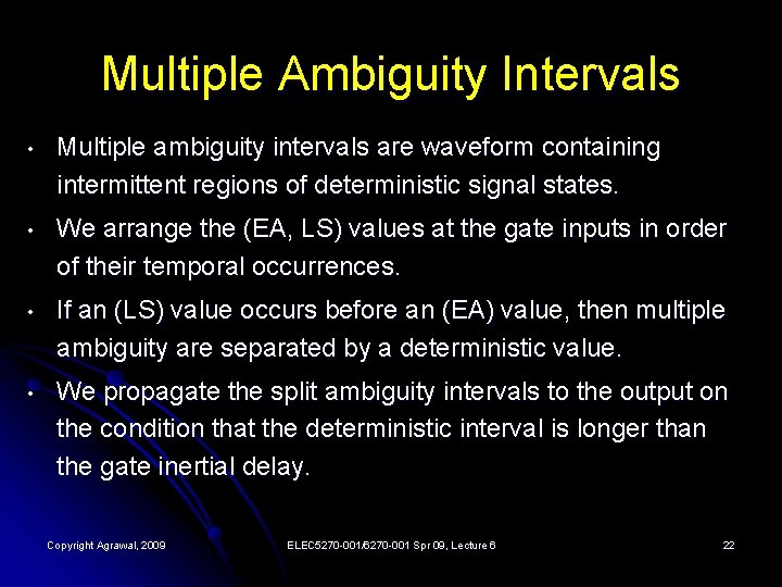
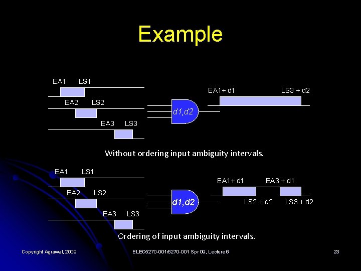
Multiple Ambiguity Intervals • Multiple ambiguity intervals are waveform containing intermittent regions of deterministic signal states. • We arrange the (EA, LS) values at the gate inputs in order of their temporal occurrences. • If an (LS) value occurs before an (EA) value, then multiple ambiguity are separated by a deterministic value. • We propagate the split ambiguity intervals to the output on the condition that the deterministic interval is longer than the gate inertial delay. Copyright Agrawal, 2009 ELEC 5270 -001/6270 -001 Spr 09, Lecture 6 22

Example EA 1 LS 1 EA 1+ d 1 EA 2 LS 3 + d 2 LS 2 d 1, d 2 EA 3 LS 3 Without ordering input ambiguity intervals. EA 1 LS 1 EA 1+ d 1 EA 2 EA 3 + d 1 LS 2 d 1, d 2 EA 3 LS 2 + d 2 LS 3 Ordering of input ambiguity intervals. Copyright Agrawal, 2009 ELEC 5270 -001/6270 -001 Spr 09, Lecture 6 23

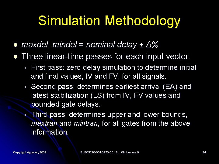
Simulation Methodology l l maxdel, mindel = nominal delay ± Δ% Three linear-time passes for each input vector: § § § First pass: zero delay simulation to determine initial and final values, IV and FV, for all signals. Second pass: determines earliest arrival (EA) and latest stabilization (LS) from IV, FV values and bounded gate delays. Third pass: determines upper and lower bounds, maxtran and mintran, for all gates from the above information. Copyright Agrawal, 2009 ELEC 5270 -001/6270 -001 Spr 09, Lecture 6 24

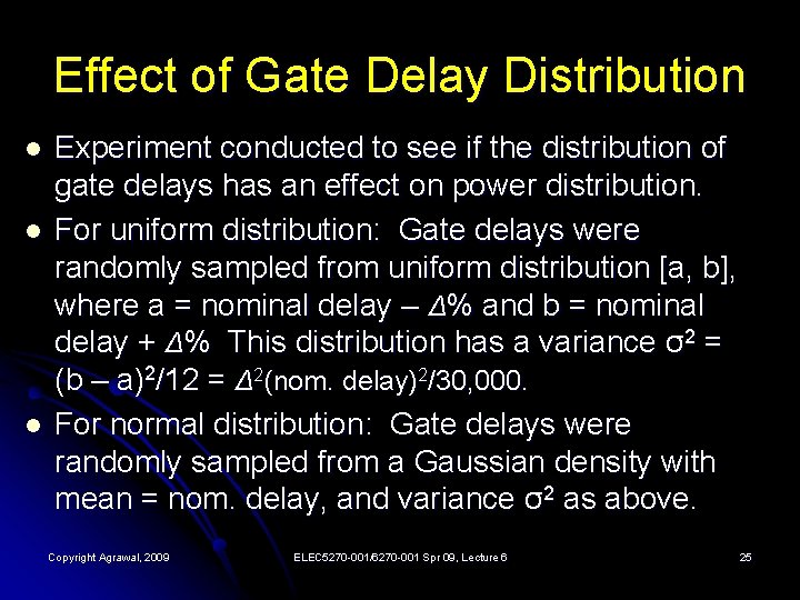
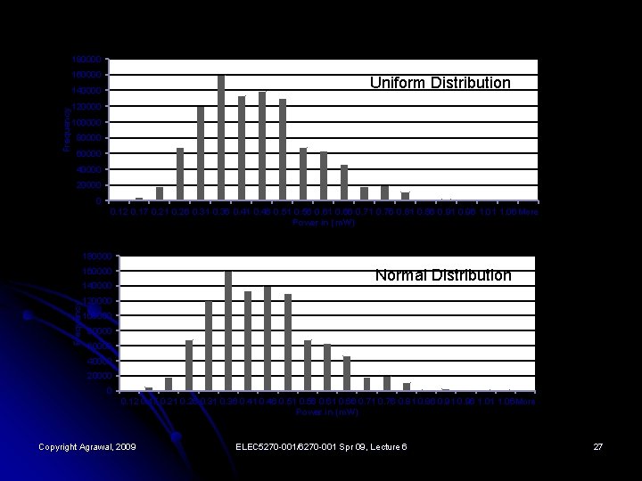
Effect of Gate Delay Distribution l l l Experiment conducted to see if the distribution of gate delays has an effect on power distribution. For uniform distribution: Gate delays were randomly sampled from uniform distribution [a, b], where a = nominal delay – Δ% and b = nominal delay + Δ% This distribution has a variance σ2 = (b – a)2/12 = Δ 2(nom. delay)2/30, 000. For normal distribution: Gate delays were randomly sampled from a Gaussian density with mean = nom. delay, and variance σ2 as above. Copyright Agrawal, 2009 ELEC 5270 -001/6270 -001 Spr 09, Lecture 6 25

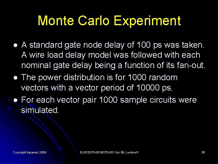
Monte Carlo Experiment l l l A standard gate node delay of 100 ps was taken. A wire load delay model was followed with each nominal gate delay being a function of its fan-out. The power distribution is for 1000 random vectors with a vector period of 10000 ps. For each vector pair 1000 sample circuits were simulated. Copyright Agrawal, 2009 ELEC 5270 -001/6270 -001 Spr 09, Lecture 6 26

180000 160000 Uniform Distribution Frequency 140000 120000 100000 80000 60000 40000 20000 0 0. 12 0. 17 0. 21 0. 26 0. 31 0. 36 0. 41 0. 46 0. 51 0. 56 0. 61 0. 66 0. 71 0. 76 0. 81 0. 86 0. 91 0. 96 1. 01 1. 06 More Power in (m. W) 180000 160000 Normal Distribution Frequency 140000 120000 100000 80000 60000 40000 20000 0 0. 12 0. 17 0. 21 0. 26 0. 31 0. 36 0. 41 0. 46 0. 51 0. 56 0. 61 0. 66 0. 71 0. 76 0. 81 0. 86 0. 91 0. 96 1. 01 1. 06 More Power in (m. W) Copyright Agrawal, 2009 ELEC 5270 -001/6270 -001 Spr 09, Lecture 6 27

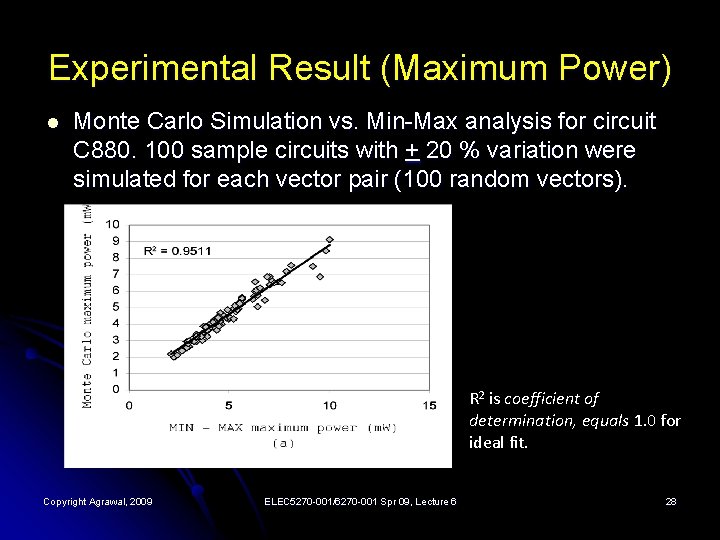
Experimental Result (Maximum Power) l Monte Carlo Simulation vs. Min-Max analysis for circuit C 880. 100 sample circuits with + 20 % variation were simulated for each vector pair (100 random vectors). R 2 is coefficient of determination, equals 1. 0 for ideal fit. Copyright Agrawal, 2009 ELEC 5270 -001/6270 -001 Spr 09, Lecture 6 28

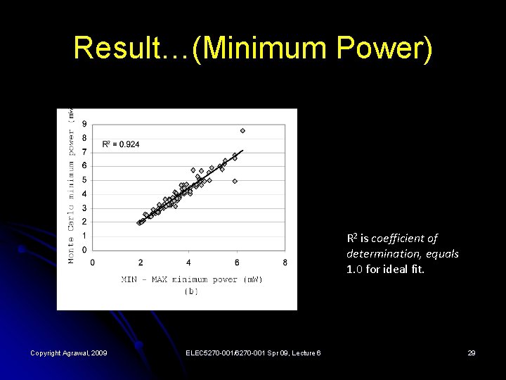
Result…(Minimum Power) R 2 is coefficient of determination, equals 1. 0 for ideal fit. Copyright Agrawal, 2009 ELEC 5270 -001/6270 -001 Spr 09, Lecture 6 29

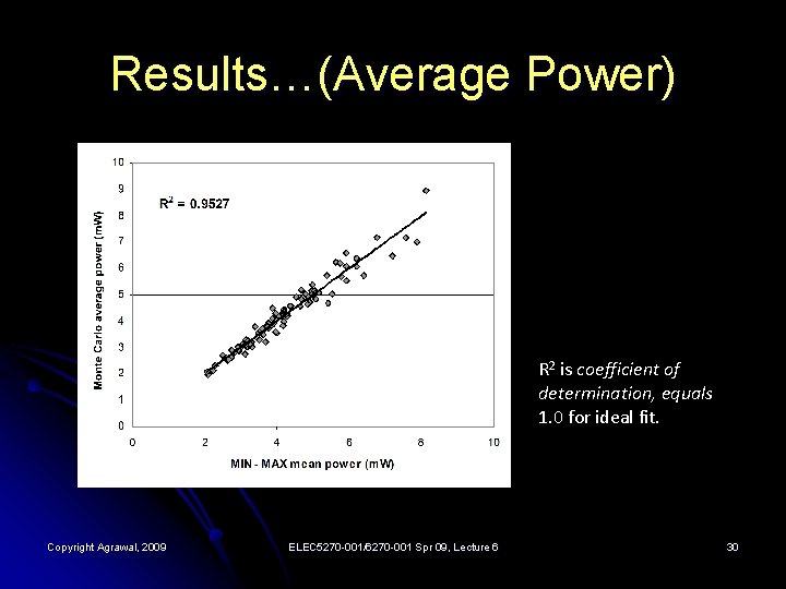
Results…(Average Power) R 2 is coefficient of determination, equals 1. 0 for ideal fit. Copyright Agrawal, 2009 ELEC 5270 -001/6270 -001 Spr 09, Lecture 6 30

C 880: Monte Carlo vs. Bounded Delay Analysis 1000 Random Vectors, 1000 Sample Circuits Monte Carlo Simulation Bounded Delay Analysis Min Power (m. W) Max Power (m. W) CPU Time (secs) 1. 42 11. 59 262. 7 1. 35 11. 89 0. 3 Copyright Agrawal, 2009 ELEC 5270 -001/6270 -001 Spr 09, Lecture 6 31

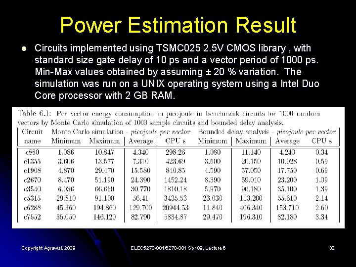
Power Estimation Result l Circuits implemented using TSMC 025 2. 5 V CMOS library , with standard size gate delay of 10 ps and a vector period of 1000 ps. Min-Max values obtained by assuming ± 20 % variation. The simulation was run on a UNIX operating system using a Intel Duo Core processor with 2 GB RAM. Copyright Agrawal, 2009 ELEC 5270 -001/6270 -001 Spr 09, Lecture 6 32

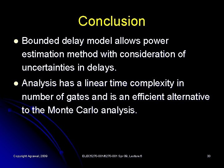
Conclusion l Bounded delay model allows power estimation method with consideration of uncertainties in delays. l Analysis has a linear time complexity in number of gates and is an efficient alternative to the Monte Carlo analysis. Copyright Agrawal, 2009 ELEC 5270 -001/6270 -001 Spr 09, Lecture 6 33

Future Refinements l l Consider process dependent variations in leakage and in node capacitances. Use statistical methods to determine distributions of average and peak power consuming circuits. See following references: l V. Bartkute and L. Sakalauskas, “Three Parameter Estimation of the Weibull Distribution by Order Statistics, ” in C. H. Skiadas, editor, Recent Advances in Stochastic Modeling and Data Analysis, pp. 91– 100, World Scientific, 2007. l Q. Qiu, Q. Wu, and M. Pedram, “Maximum power estimation using the limiting distributions of extreme order statistics, ” in Proc. Design Automation Conference, June 1998, pp. 684– 689. Q. Wu, Q. Qiu, and M. Pedram, “Estimation of Peak Power Dissipation in VLSI Circuits Using the Limiting Distributions of Extreme Order Statistics, ” IEEE transactions on Computer Aided Design of Integrated Circuits and Systems, vol. 20, no. 8, p. 942. l Copyright Agrawal, 2009 ELEC 5270 -001/6270 -001 Spr 09, Lecture 6 34