ELEC 52706270 Spring 2011 LowPower Design of Electronic
![i(t) = C dv(t)/dt = [V – v(t)] /R dv(t) V – v(t) ─── i(t) = C dv(t)/dt = [V – v(t)] /R dv(t) V – v(t) ───](https://slidetodoc.com/presentation_image_h2/d635988f2c1d5c3a4ef611c767e8fb5b/image-9.jpg)
![v(t) = i(t) Copyright Agrawal, 2007 = –t V [1 – exp( ── )] v(t) = i(t) Copyright Agrawal, 2007 = –t V [1 – exp( ── )]](https://slidetodoc.com/presentation_image_h2/d635988f2c1d5c3a4ef611c767e8fb5b/image-10.jpg)
![i(t) = C dv(t)/dt = dv(t) ─── dt = [V(t) – v(t)] /R V(t) i(t) = C dv(t)/dt = dv(t) ─── dt = [V(t) – v(t)] /R V(t)](https://slidetodoc.com/presentation_image_h2/d635988f2c1d5c3a4ef611c767e8fb5b/image-15.jpg)
![Constant Current Is Optimum I(t) R t = [0, T] V C Copyright Agrawal, Constant Current Is Optimum I(t) R t = [0, T] V C Copyright Agrawal,](https://slidetodoc.com/presentation_image_h2/d635988f2c1d5c3a4ef611c767e8fb5b/image-17.jpg)
- Slides: 34

ELEC 5270/6270 Spring 2011 Low-Power Design of Electronic Circuits Adiabatic Logic Vishwani D. Agrawal James J. Danaher Professor Dept. of Electrical and Computer Engineering Auburn University, Auburn, AL 36849 vagrawal@eng. auburn. edu http: //www. eng. auburn. edu/~vagrawal/COURSE/E 6270_Spr 11/course. html Copyright Agrawal, 2007 ELEC 6270 Spring 11, Lecture 8 1

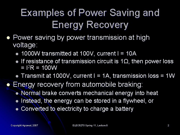
Examples of Power Saving and Energy Recovery l Power saving by power transmission at high voltage: l l 1000 W transmitted at 100 V, current I = 10 A If resistance of transmission circuit is 1Ω, then power loss = I 2 R = 100 W Transmit at 1000 V, current I = 1 A, transmission loss = 1 W Energy recovery from automobile braking: l l l Normal brake converts mechanical energy into heat Instead, the energy can be stored in a flywheel, or Converted to electricity to charge a battery Copyright Agrawal, 2007 ELEC 6270 Spring 11, Lecture 8 2

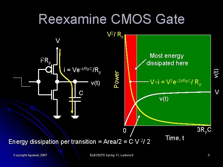
Reexamine CMOS Gate V 2 / R p V Most energy dissipated here i = Ve–t/Rp. C/Rp v(t) p Power i 2 R V×i = V 2 e– 2 t/Rp. C/ Rp C v(t) 3 Rp. C 0 Energy dissipation per transition = Area/2 = C V 2/ 2 Copyright Agrawal, 2007 V ELEC 6270 Spring 11, Lecture 8 Time, t 3

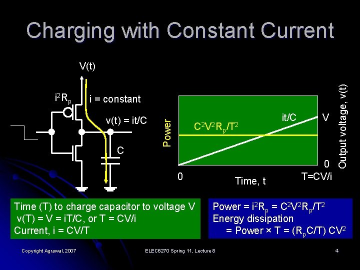
Charging with Constant Current i = constant v(t) = it/C C Power i 2 Rp C 2 V 2 R 0 Time (T) to charge capacitor to voltage V v(T) = V = i. T/C, or T = CV/i Current, i = CV/T Copyright Agrawal, 2007 p /T 2 Time, t it/C V 0 T=CV/i Output voltage, v(t) V(t) Power = i 2 Rp = C 2 V 2 Rp/T 2 Energy dissipation = Power × T = (Rp. C/T) CV 2 ELEC 6270 Spring 11, Lecture 8 4

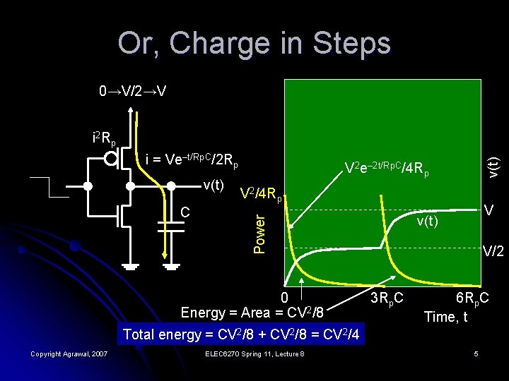
Or, Charge in Steps 0→V/2→V i = Ve–t/Rp. C/2 Rp C V 2 e– 2 t/Rp. C/4 Rp V 2/4 Rp 0 Energy = Area = CV 2/8 V v(t) Power v(t) i 2 Rp V/2 3 Rp. C 6 Rp. C Time, t Total energy = CV 2/8 + CV 2/8 = CV 2/4 Copyright Agrawal, 2007 ELEC 6270 Spring 11, Lecture 8 5

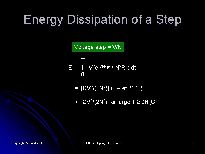
Energy Dissipation of a Step Voltage step = V/N T E = ∫ V 2 e– 2 t/Rp. C/(N 2 Rp) dt 0 = [CV 2/(2 N 2)] (1 – e– 2 T/Rp. C) ≈ CV 2/(2 N 2) for large T ≥ 3 Rp. C Copyright Agrawal, 2007 ELEC 6270 Spring 11, Lecture 8 6

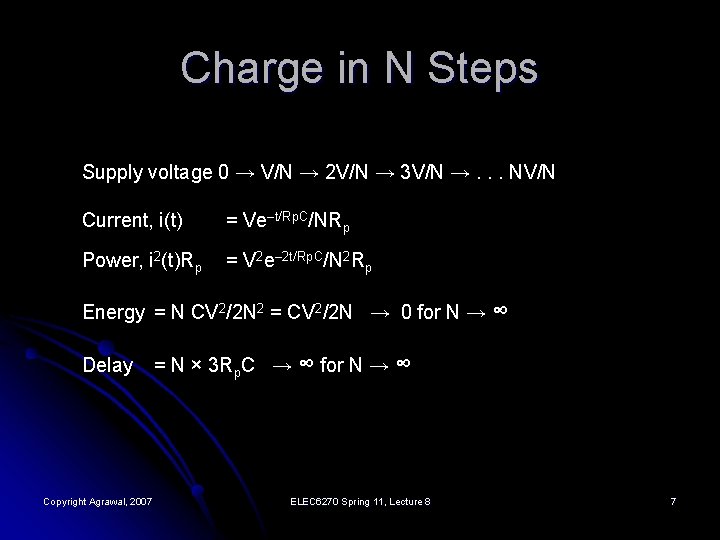
Charge in N Steps Supply voltage 0 → V/N → 2 V/N → 3 V/N →. . . NV/N Current, i(t) = Ve–t/Rp. C/NRp Power, i 2(t)Rp = V 2 e– 2 t/Rp. C/N 2 Rp Energy = N CV 2/2 N 2 = CV 2/2 N → 0 for N → ∞ Delay Copyright Agrawal, 2007 = N × 3 Rp. C → ∞ for N → ∞ ELEC 6270 Spring 11, Lecture 8 7

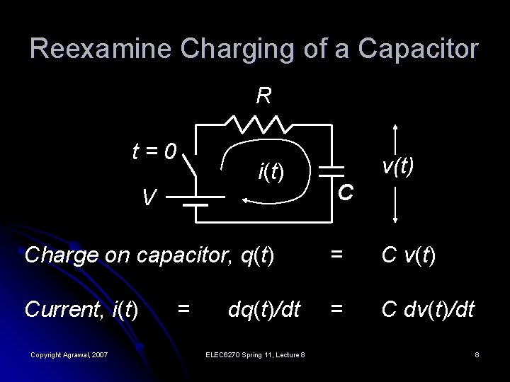
Reexamine Charging of a Capacitor R t=0 i(t) V v(t) C Charge on capacitor, q(t) = C v(t) Current, i(t) = C dv(t)/dt Copyright Agrawal, 2007 = dq(t)/dt ELEC 6270 Spring 11, Lecture 8 8
![it C dvtdt V vt R dvt V vt i(t) = C dv(t)/dt = [V – v(t)] /R dv(t) V – v(t) ───](https://slidetodoc.com/presentation_image_h2/d635988f2c1d5c3a4ef611c767e8fb5b/image-9.jpg)
i(t) = C dv(t)/dt = [V – v(t)] /R dv(t) V – v(t) ─── = ───── dt RC dv(t) dt ∫ ───── = ∫ ──── V – v(t) RC –t ln [V – v(t)] = ── + A RC Initial condition, t = 0, v(t) = 0 → A = ln V –t v(t) = V [1 – exp(───)] RC Copyright Agrawal, 2007 ELEC 6270 Spring 11, Lecture 8 9
![vt it Copyright Agrawal 2007 t V 1 exp v(t) = i(t) Copyright Agrawal, 2007 = –t V [1 – exp( ── )]](https://slidetodoc.com/presentation_image_h2/d635988f2c1d5c3a4ef611c767e8fb5b/image-10.jpg)
v(t) = i(t) Copyright Agrawal, 2007 = –t V [1 – exp( ── )] RC dv(t) C ─── dt = ELEC 6270 Spring 11, Lecture 8 V –t ── exp( ── ) R RC 10

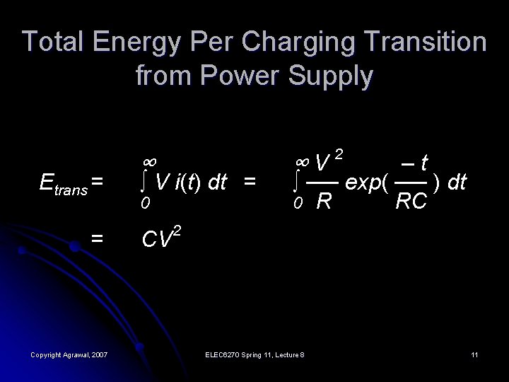
Total Energy Per Charging Transition from Power Supply Etrans = = Copyright Agrawal, 2007 ∞ ∫ V i(t) dt = 0 CV ∞V 2 –t ∫ ── exp( ── ) dt 0 R RC 2 ELEC 6270 Spring 11, Lecture 8 11

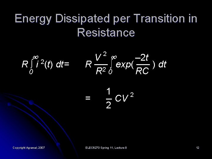
Energy Dissipated per Transition in Resistance ∞ V ∞ – 2 t R ── ∫ exp( ── ) dt 2 R 0 RC 2 2 R ∫ i (t) dt= 0 = Copyright Agrawal, 2007 1 2 ─ CV 2 ELEC 6270 Spring 11, Lecture 8 12

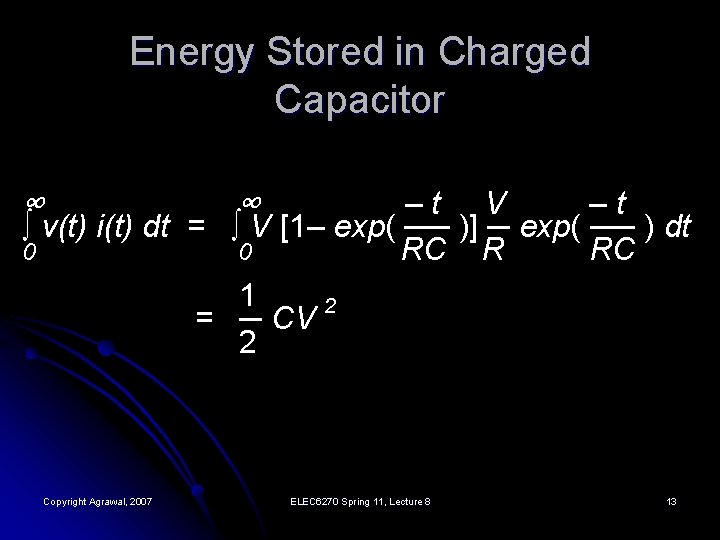
Energy Stored in Charged Capacitor ∞ ∞ –t V –t ∫ v(t) i(t) dt = ∫ V [1– exp( ── )] ─ exp( ── ) dt 0 0 RC R RC 1 2 = ─ CV 2 Copyright Agrawal, 2007 ELEC 6270 Spring 11, Lecture 8 13

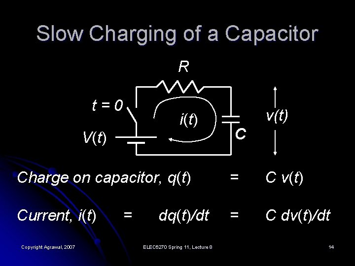
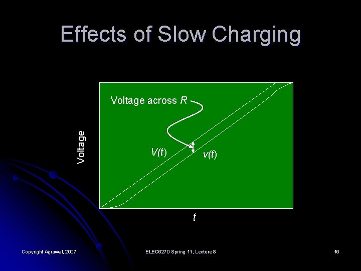
Slow Charging of a Capacitor R t=0 i(t) V(t) v(t) C Charge on capacitor, q(t) = C v(t) Current, i(t) = C dv(t)/dt Copyright Agrawal, 2007 = dq(t)/dt ELEC 6270 Spring 11, Lecture 8 14
![it C dvtdt dvt dt Vt vt R Vt i(t) = C dv(t)/dt = dv(t) ─── dt = [V(t) – v(t)] /R V(t)](https://slidetodoc.com/presentation_image_h2/d635988f2c1d5c3a4ef611c767e8fb5b/image-15.jpg)
i(t) = C dv(t)/dt = dv(t) ─── dt = [V(t) – v(t)] /R V(t) – v(t) ───── RC dv(t) dt ∫ ────── = ∫ ──── V(t) – v(t) RC Copyright Agrawal, 2007 ELEC 6270 Spring 11, Lecture 8 15

Effects of Slow Charging Voltage across R V(t) v(t) t Copyright Agrawal, 2007 ELEC 6270 Spring 11, Lecture 8 16
![Constant Current Is Optimum It R t 0 T V C Copyright Agrawal Constant Current Is Optimum I(t) R t = [0, T] V C Copyright Agrawal,](https://slidetodoc.com/presentation_image_h2/d635988f2c1d5c3a4ef611c767e8fb5b/image-17.jpg)
Constant Current Is Optimum I(t) R t = [0, T] V C Copyright Agrawal, 2007 ELEC 6270 Spring 11, Lecture 8 17

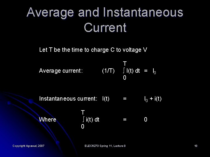
Average and Instantaneous Current Let T be the time to charge C to voltage V Average current: (1/T) Instantaneous current: I(t) Where Copyright Agrawal, 2007 T ∫ i(t) dt 0 T ∫ I(t) dt = I 0 0 = I 0 + i(t) = 0 ELEC 6270 Spring 11, Lecture 8 18

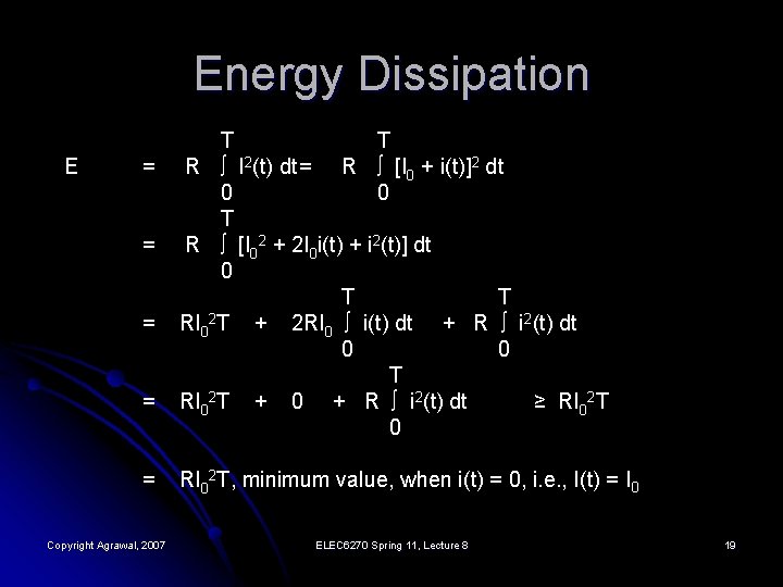
Energy Dissipation E = = = Copyright Agrawal, 2007 T T R ∫ I 2(t) dt= R ∫ [I 0 + i(t)]2 dt 0 0 T R ∫ [I 02 + 2 I 0 i(t) + i 2(t)] dt 0 T T RI 02 T + 2 RI 0 ∫ i(t) dt + R ∫ i 2(t) dt 0 0 T RI 02 T + 0 + R ∫ i 2(t) dt ≥ RI 02 T 0 RI 02 T, minimum value, when i(t) = 0, i. e. , I(t) = I 0 ELEC 6270 Spring 11, Lecture 8 19

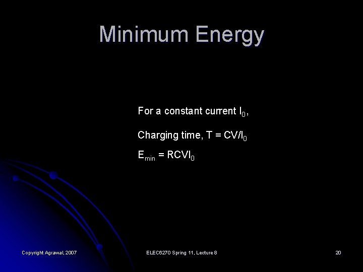
Minimum Energy For a constant current I 0, Charging time, T = CV/I 0 Emin = RCVI 0 Copyright Agrawal, 2007 ELEC 6270 Spring 11, Lecture 8 20

References l l C. L. Seitz, A. H. Frey, S. Mattisson, S. D. Rabin, D. A. Speck and J. L. A. van de Snepscheut, “Hot-Clock n. MOS, ” Proc. Chapel Hill Conf. VLSI, 1985, pp. 1 -17. W. C. Athas, L. J. Swensson, J. D. Koller, N. Tzartzanis and E. Y. -C. Chou, “Low-Power Digital Systems Based on Adiabatic-Switching Principles, ” IEEE Trans. VLSI Systems, vol. 2, no. 4, pp. 398 -407, Dec. 1994. Copyright Agrawal, 2007 ELEC 6270 Spring 11, Lecture 8 21

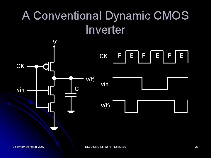
A Conventional Dynamic CMOS Inverter V CK P E P E CK v(t) vin C vin v(t) Copyright Agrawal, 2007 ELEC 6270 Spring 11, Lecture 8 22

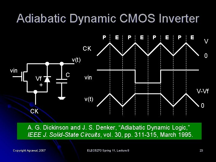
Adiabatic Dynamic CMOS Inverter P E P E V CK 0 v(t) vin Vf + C vin V-Vf v(t) CK 0 A. G. Dickinson and J. S. Denker, “Adiabatic Dynamic Logic, ” IEEE J. Solid-State Circuits, vol. 30, pp. 311 -315, March 1995. Copyright Agrawal, 2007 ELEC 6270 Spring 11, Lecture 8 23

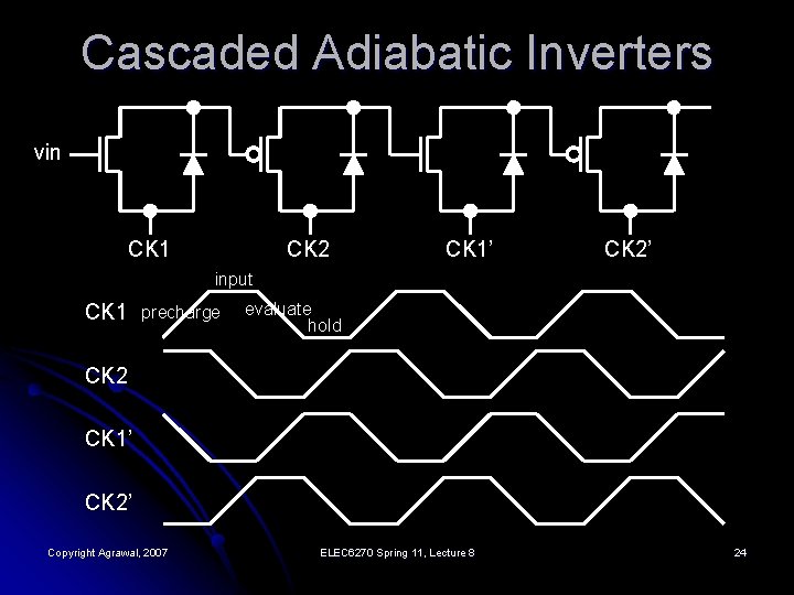
Cascaded Adiabatic Inverters vin CK 1 CK 2 CK 1’ CK 2’ input CK 1 precharge evaluate hold CK 2 CK 1’ CK 2’ Copyright Agrawal, 2007 ELEC 6270 Spring 11, Lecture 8 24

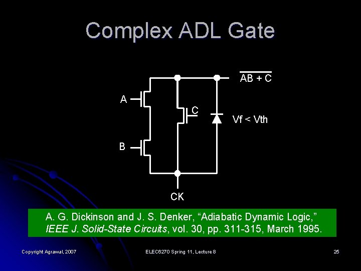
Complex ADL Gate AB + C A C Vf < Vth B CK A. G. Dickinson and J. S. Denker, “Adiabatic Dynamic Logic, ” IEEE J. Solid-State Circuits, vol. 30, pp. 311 -315, March 1995. Copyright Agrawal, 2007 ELEC 6270 Spring 11, Lecture 8 25

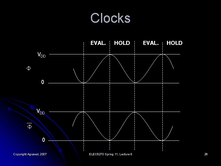
Clocks EVAL. HOLD VDD 0 Copyright Agrawal, 2007 ELEC 6270 Spring 11, Lecture 8 26

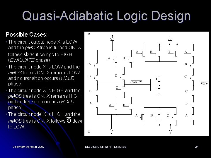
Quasi-Adiabatic Logic Design Possible Cases: • The circuit output node X is LOW and the p. MOS tree is turned ON: X follows as it swings to HIGH (EVALUATE phase) • The circuit node X is LOW and the n. MOS tree is ON. X remains LOW and no transition occurs (HOLD phase) • The circuit node X is HIGH and the p. MOS tree is ON. X remains HIGH and no transition occurs (HOLD phase) • The circuit node X is HIGH and the n. MOS tree is ON. X follows down to LOW. Copyright Agrawal, 2007 ELEC 6270 Spring 11, Lecture 8 27

A Case Study K. Parameswaran, “Low Power Design of a 32 -bit Quasi-Adiabatic ARM Based Microprocessor, ” Master’s Thesis, Dept. of ECE, Rutgers University, New Brunswick, NJ, 2004. Copyright Agrawal, 2007 ELEC 6270 Spring 11, Lecture 8 28

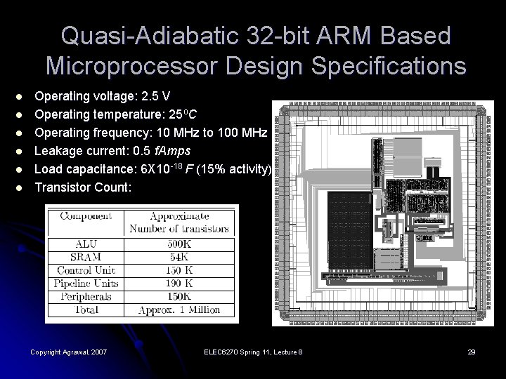
Quasi-Adiabatic 32 -bit ARM Based Microprocessor Design Specifications l l l Operating voltage: 2. 5 V Operating temperature: 25 o. C Operating frequency: 10 MHz to 100 MHz Leakage current: 0. 5 f. Amps Load capacitance: 6 X 10 -18 F (15% activity) Transistor Count: Copyright Agrawal, 2007 ELEC 6270 Spring 11, Lecture 8 29

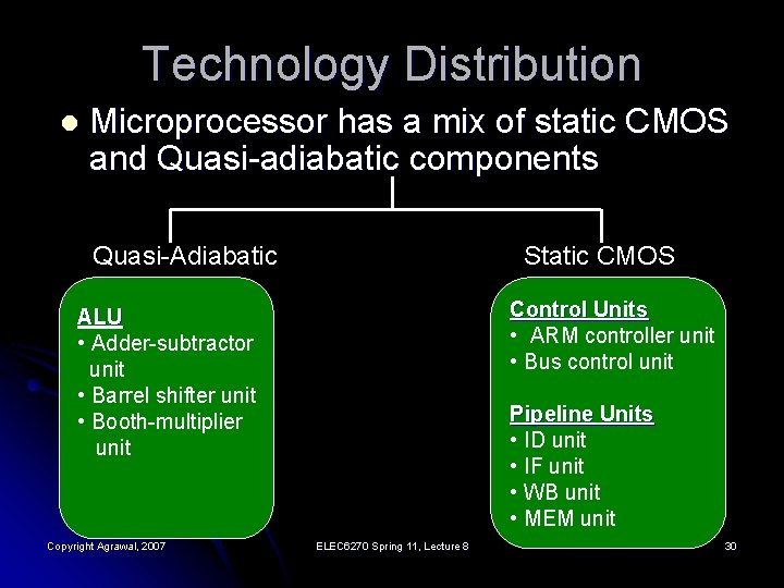
Technology Distribution l Microprocessor has a mix of static CMOS and Quasi-adiabatic components Quasi-Adiabatic Static CMOS Control Units • ARM controller unit • Bus control unit ALU • Adder-subtractor unit • Barrel shifter unit • Booth-multiplier unit Copyright Agrawal, 2007 Pipeline Units • ID unit • IF unit • WB unit • MEM unit ELEC 6270 Spring 11, Lecture 8 30

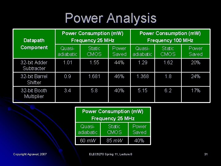
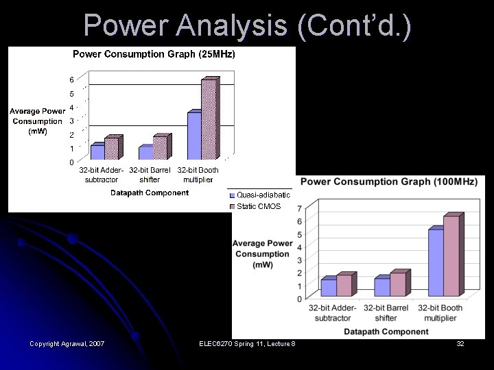
Power Analysis Datapath Component Power Consumption (m. W) Frequency 25 MHz Power Consumption (m. W) Frequency 100 MHz Quasiadiabatic Static CMOS Power Saved 32 -bit Adder Subtracter 1. 01 1. 55 44% 1. 29 1. 62 20% 32 -bit Barrel Shifter 0. 9 1. 681 46% 1. 368 1. 8 24% 32 -bit Booth Multiplier 3. 4 5. 8 40% 5. 15 6. 2 17% Power Consumption (m. W) Frequency 25 MHz Copyright Agrawal, 2007 Quasiadiabatic Static CMOS Power Saved 60 m. W 85 m. W 40% ELEC 6270 Spring 11, Lecture 8 31

Power Analysis (Cont’d. ) Copyright Agrawal, 2007 ELEC 6270 Spring 11, Lecture 8 32

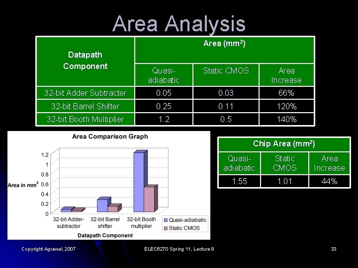
Area Analysis Area (mm 2) Datapath Component Quasiadiabatic Static CMOS Area Increase 32 -bit Adder Subtracter 0. 05 0. 03 66% 32 -bit Barrel Shifter 0. 25 0. 11 120% 32 -bit Booth Multiplier 1. 2 0. 5 140% Chip Area (mm 2) Copyright Agrawal, 2007 ELEC 6270 Spring 11, Lecture 8 Quasiadiabatic Static CMOS Area Increase 1. 55 1. 01 44% 33

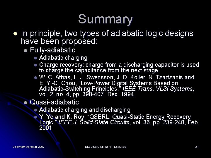
Summary l In principle, two types of adiabatic logic designs have been proposed: l Fully-adiabatic Adiabatic charging l Charge recovery: charge from a discharging capacitor is used to charge the capacitance from the next stage. l W. C. Athas, L. J. Swensson, J. D. Koller, N. Tzartzanis and E. Y. -C. Chou, “Low-Power Digital Systems Based on Adiabatic-Switching Principles, ” IEEE Trans. VLSI Systems, vol. 2, no. 4, pp. 398 -407, Dec. 1994. l l Quasi-adiabatic Adiabatic charging and discharging l Y. Ye and K. Roy, “QSERL: Quasi-Static Energy Recovery Logic, ” IEEE J. Solid-State Circuits, vol. 36, pp. 239 -248, Feb. 2001. l Copyright Agrawal, 2007 ELEC 6270 Spring 11, Lecture 8 34