Detector Technologies for WSO Jon Lapington Space Research
- Slides: 28

Detector Technologies for WSO Jon Lapington Space Research Centre University of Leicester 3 -5 December, 2007 WSO Detector Workshop, Leicester

Outline • • Choice of detector: MCPs or CCDs? MCP detectors Photocathodes Microchannel plates Image readout devices The Vernier Anode Image Charge technique Readout developments 3 -5 December, 2007 WSO Detector Workshop, Leicester

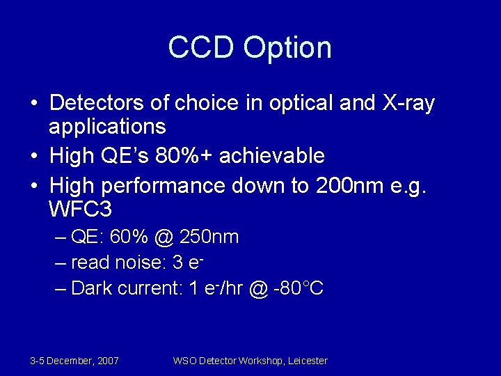
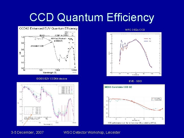
CCD Option • Detectors of choice in optical and X-ray applications • High QE’s 80%+ achievable • High performance down to 200 nm e. g. WFC 3 – QE: 60% @ 250 nm – read noise: 3 e– Dark current: 1 e-/hr @ -80°C 3 -5 December, 2007 WSO Detector Workshop, Leicester

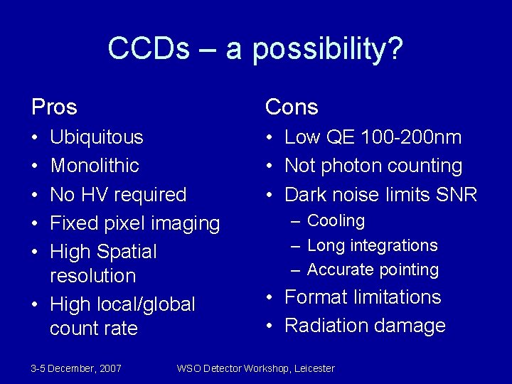
CCDs – a possibility? Pros Cons • • • Low QE 100 -200 nm • Not photon counting • Dark noise limits SNR Ubiquitous Monolithic No HV required Fixed pixel imaging High Spatial resolution • High local/global count rate 3 -5 December, 2007 – Cooling – Long integrations – Accurate pointing • Format limitations • Radiation damage WSO Detector Workshop, Leicester

CCD Quantum Efficiency WFC-3 E 2 v CCD GOES E 2 V CCD 64 device 3 -5 December, 2007 WSO Detector Workshop, Leicester EVE - SDO

MCPs –preferred Pros Cons • • • HV required • Vacuum/hermetically sealed pre-launch • Contamination sensitive • Ageing – gain depression • Over-bright shutdown • Local count rate limitation True photon counting Flexible format Mature technology High spatial resolution High temporal resolution QE 30 - 40% for LSS λ Low background No cooling Radiation hard 3 -5 December, 2007 WSO Detector Workshop, Leicester

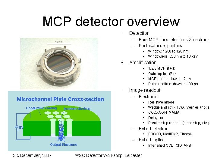
MCP detector overview • Detection – Bare MCP: ions, electrons & neutrons – Photocathode: photons • • • Amplification • • • PHOTOCATHODE Microchannel Plate Cross-section Conductive coating HV + e- 1/2/3 MCP stack Gain: up to 108 e. MCP pore ø: down to 2µm Pulse risetime: down to ~80 ps Image readout – Electronic: • • • Incident electron 104 -108 e- Window: 1200 to 120 nm Windowless: 200 nm to 10 ke. V Resistive anode Wedge and strip, TWA, Vernier anode CODACON, MAMA Delay line Parallel strip readout (cross strip, etc. ) – Hybrid: electronic • EBCCD, Medi. Pix 2, Timepix – Hybrid: optical Output Electrons 3 -5 December, 2007 WSO Detector Workshop, Leicester • Intensified CCD, CID, APS

Photocathodes • Event detection via photoelectron released from a photocathode • Windowed - above 120 nm – Semi-transparent photocathode – Alkali halide, bi-alkali, multi-alkali S 20, Ga. As (NEA) – QE – up to 25 -30 % • Windowless - below 250 nm – – – opaque photocathode deposited directly on MCP Cs. I, KBr, Cs. Te, (Ga. N), (Diamond) etc Alkali halides up to 50% in XUV Ga. N – 71 % reported Response up to 10 ke. V Poor energy resolution in X-rays 3 -5 December, 2007 WSO Detector Workshop, Leicester

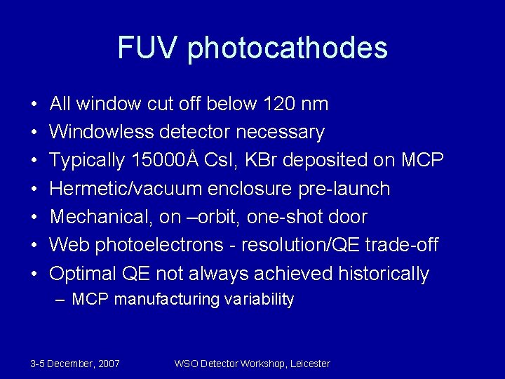
FUV photocathodes • • All window cut off below 120 nm Windowless detector necessary Typically 15000Å Cs. I, KBr deposited on MCP Hermetic/vacuum enclosure pre-launch Mechanical, on –orbit, one-shot door Web photoelectrons - resolution/QE trade-off Optimal QE not always achieved historically – MCP manufacturing variability 3 -5 December, 2007 WSO Detector Workshop, Leicester

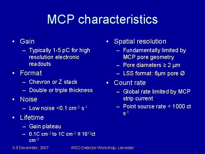
MCP characteristics • Gain • Spatial resolution – Typically 1 -5 p. C for high resolution electronic readouts • Format – Chevron or Z stack – Double or triple thickness • Noise – Low noise <0. 1 cm-2 s-1 • Lifetime – Fundamentally limited by MCP pore geometry – Pore diameters ≥ 2 µm – LSS format: 6µm pore Ø • Count rate – Global rate limited by MCP strip current – Point source rate < 1000 ct s-1 – Gain plateau – 0. 1 C cm-2 to 1 C cm-2 ≡ 1012 ct cm-2 3 -5 December, 2007 WSO Detector Workshop, Leicester

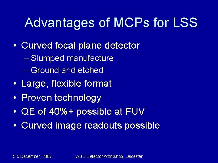
Advantages of MCPs for LSS • Curved focal plane detector – Slumped manufacture – Ground and etched • • Large, flexible format Proven technology QE of 40%+ possible at FUV Curved image readouts possible 3 -5 December, 2007 WSO Detector Workshop, Leicester

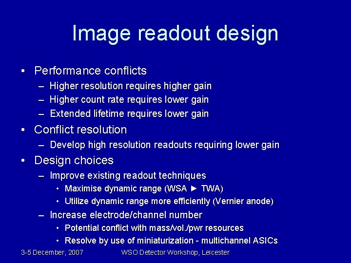
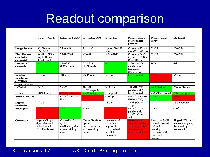
Image readout design • Performance conflicts – Higher resolution requires higher gain – Higher count rate requires lower gain – Extended lifetime requires lower gain • Conflict resolution – Develop high resolution readouts requiring lower gain • Design choices – Improve existing readout techniques • Maximise dynamic range (WSA ► TWA) • Utilize dynamic range more efficiently (Vernier anode) – Increase electrode/channel number • Potential conflict with mass/vol. /pwr resources • Resolve by use of miniaturization - multichannel ASICs 3 -5 December, 2007 WSO Detector Workshop, Leicester

Readout comparison 3 -5 December, 2007 WSO Detector Workshop, Leicester

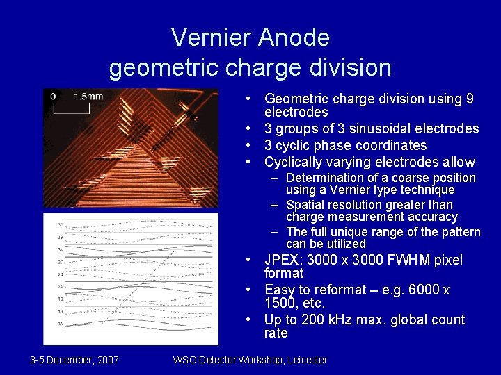
Vernier Anode geometric charge division • Geometric charge division using 9 electrodes • 3 groups of 3 sinusoidal electrodes • 3 cyclic phase coordinates • Cyclically varying electrodes allow – Determination of a coarse position using a Vernier type technique – Spatial resolution greater than charge measurement accuracy – The full unique range of the pattern can be utilized • JPEX: 3000 x 3000 FWHM pixel format • Easy to reformat – e. g. 6000 x 1500, etc. • Up to 200 k. Hz max. global count rate 3 -5 December, 2007 WSO Detector Workshop, Leicester

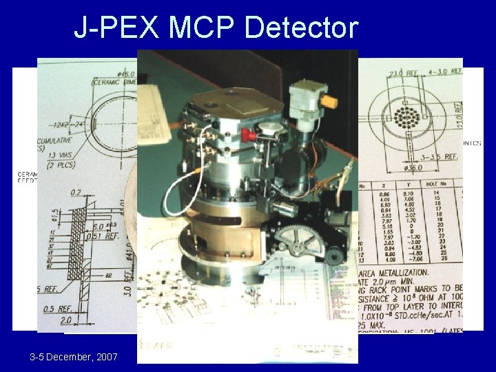
J-PEX MCP Detector 3 -5 December, 2007 WSO Detector Workshop, Leicester

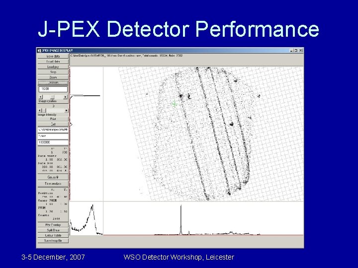
J-PEX Detector Performance 3 -5 December, 2007 WSO Detector Workshop, Leicester

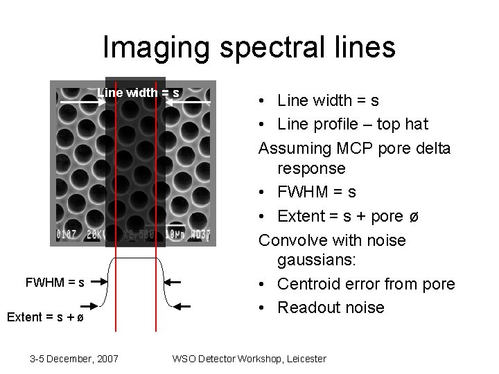
Imaging spectral lines Line width = s FWHM = s Extent = s + ø 3 -5 December, 2007 • Line width = s • Line profile – top hat Assuming MCP pore delta response • FWHM = s • Extent = s + pore ø Convolve with noise gaussians: • Centroid error from pore • Readout noise WSO Detector Workshop, Leicester

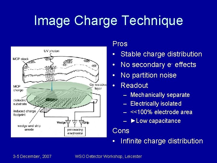
Image Charge Technique Pros • Stable charge distribution • No secondary e- effects • No partition noise • Readout – – Mechanically separate Electrically isolated <<100% electrode area ►Low capacitance Cons • Infinite charge distribution 3 -5 December, 2007 WSO Detector Workshop, Leicester

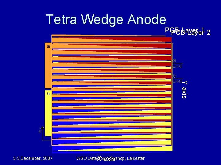
Tetra Wedge Anode PCB Layer 12 PCB Layer Y axis 3 -5 December, 2007 X axis WSO Detector Workshop, Leicester

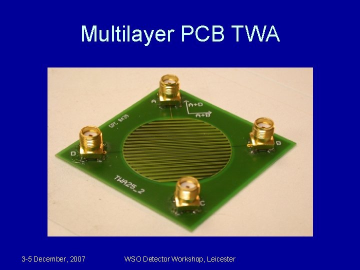
Multilayer PCB TWA 3 -5 December, 2007 WSO Detector Workshop, Leicester

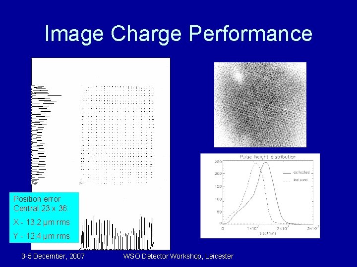
Image Charge Performance Position error Central 23 x 36: X - 13. 2 µm rms Y - 12. 4 µm rms 3 -5 December, 2007 WSO Detector Workshop, Leicester

Image Charge Optimizations • Image Charge uses capacitive coupling – – – – No direct charge collection Electrode area can be << 100% Low inter-electrode capacitance Beneficial for MCP gain/rate/lifetime trade-off Vernier redesigned as 3 sets of parallel strips Readout constructed as 3 layer flexi PCB Improved peformance due to lowered capacitance Can be simply curved to match curved focal plane/MCPs 3 -5 December, 2007 WSO Detector Workshop, Leicester 22

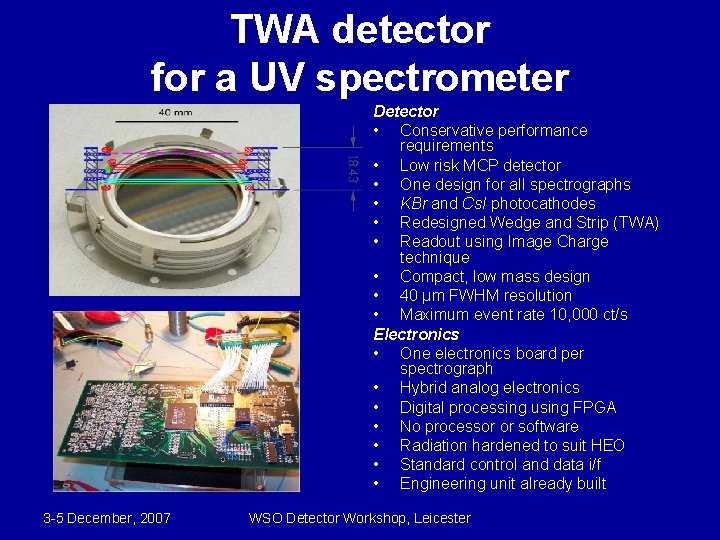
TWA detector for a UV spectrometer Detector • Conservative performance requirements • Low risk MCP detector • One design for all spectrographs • KBr and Cs. I photocathodes • Redesigned Wedge and Strip (TWA) • Readout using Image Charge technique • Compact, low mass design • 40 μm FWHM resolution • Maximum event rate 10, 000 ct/s Electronics • One electronics board per spectrograph • Hybrid analog electronics • Digital processing using FPGA • No processor or software • Radiation hardened to suit HEO • Standard control and data i/f • Engineering unit already built 3 -5 December, 2007 WSO Detector Workshop, Leicester

Charge division readout limitations • Requires accurate charge measurement – longer shaping times for adequate SNR – high MCP gain required ≥ 107 electrons – High gain MCP suffers from: • Lower local and global count rate • Shorter lifetime • Higher power requirements • Serial event processing – Readout electrodes have global scope – Detector is paralysed while each event is processed 3 -5 December, 2007 WSO Detector Workshop, Leicester

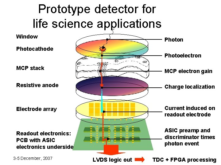
Prototype detector for life science applications Window Photon Photocathode Photoelectron MCP stack MCP electron gain Resistive anode Charge localization Electrode array Current induced on readout electrode ASIC preamp and discriminator times photon event Readout electronics: PCB with ASIC electronics underside 3 -5 December, 2007 WSO Detector Leicester LVDSWorkshop, logic out TDC + FPGA processing

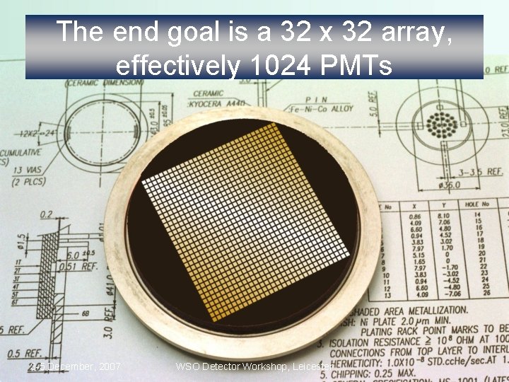
The end goal is a 32 x 32 array, effectively 1024 PMTs 3 -5 December, 2007 WSO Detector Workshop, Leicester

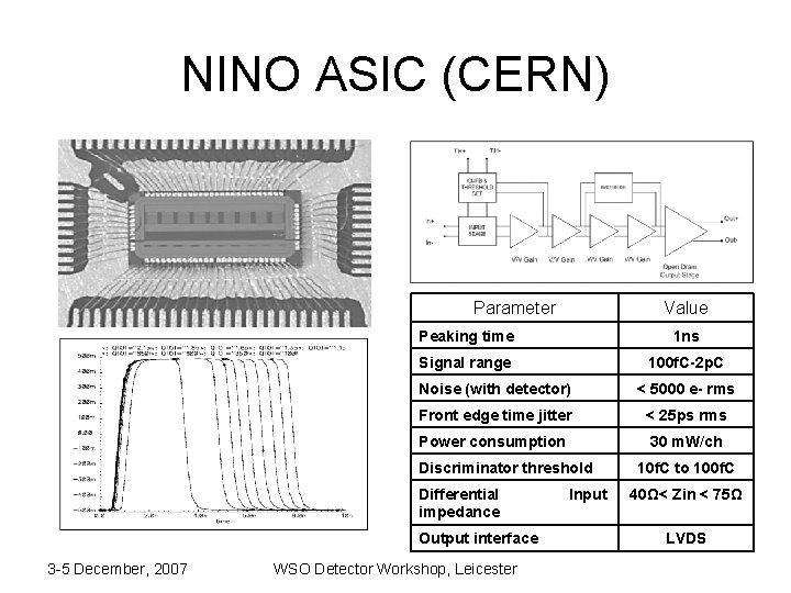
NINO ASIC (CERN) Parameter Value Peaking time 1 ns Signal range 100 f. C-2 p. C Noise (with detector) < 5000 e- rms Front edge time jitter < 25 ps rms Power consumption 30 m. W/ch Discriminator threshold Differential impedance Output interface 3 -5 December, 2007 WSO Detector Workshop, Leicester Input 10 f. C to 100 f. C 40Ω< Zin < 75Ω LVDS

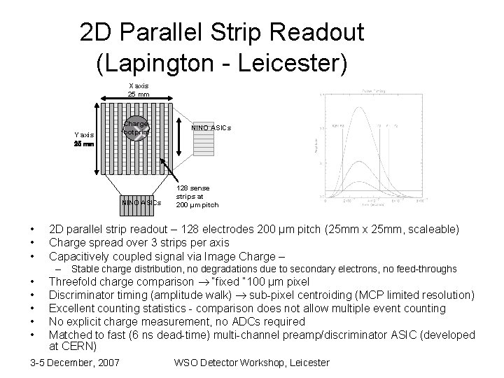
2 D Parallel Strip Readout (Lapington - Leicester) X axis 25 mm Y axis 25 mm Charge footprint NINO ASICs • • • NINO ASICs 128 sense strips at 200 μm pitch 2 D parallel strip readout – 128 electrodes 200 µm pitch (25 mm x 25 mm, scaleable) Charge spread over 3 strips per axis Capacitively coupled signal via Image Charge – – Stable charge distribution, no degradations due to secondary electrons, no feed-throughs • • • Threefold charge comparison “fixed ” 100 µm pixel Discriminator timing (amplitude walk) sub-pixel centroiding (MCP limited resolution) Excellent counting statistics - comparison does not allow multiple event counting No explicit charge measurement, no ADCs required Matched to fast (6 ns dead-time) multi-channel preamp/discriminator ASIC (developed at CERN) 3 -5 December, 2007 WSO Detector Workshop, Leicester