DETECTOR SIGNAL PROCESSING for Lar TPC Filtering and

- Slides: 73

DETECTOR SIGNAL PROCESSING for Lar TPC: Filtering and Signal to Noise Optimization Sergio Rescia and Veljko Radeka Brookhaven National Laboratory Aknowledgement: Hucheng Chen Gianluigi de Geronimo Shaorui Li Bo Yu Microboone Collaboration

DETECTOR SIGNAL PROCESSING 1. Noise Generation Mechanisms. ● Generation of noise spectra ● Random telegraph Noise (RTS) and 1/f noise 2. Equivalent Noise Charge (ENC) Calculation. ● ENC calculation in time and frequency domains ● Simple ENC calculation for series and parallel noise ● ENC Calculation for 1/f noise ● 1/f noise parameters and noise corner frequency for 1/f vs. white noise 4. Signal Processing, i. e. , "filtering" or "pulse shaping“ 5. . ● Weighting function of the whole detector readout system ● Correlated and uncorrelated sampling ● Optimum weighting functions 6. Resistive Wire Noise 7. Anti Aliasing Filter 8. Noise from Dielectrics 9. Concluding remarks 10. Appendix 2

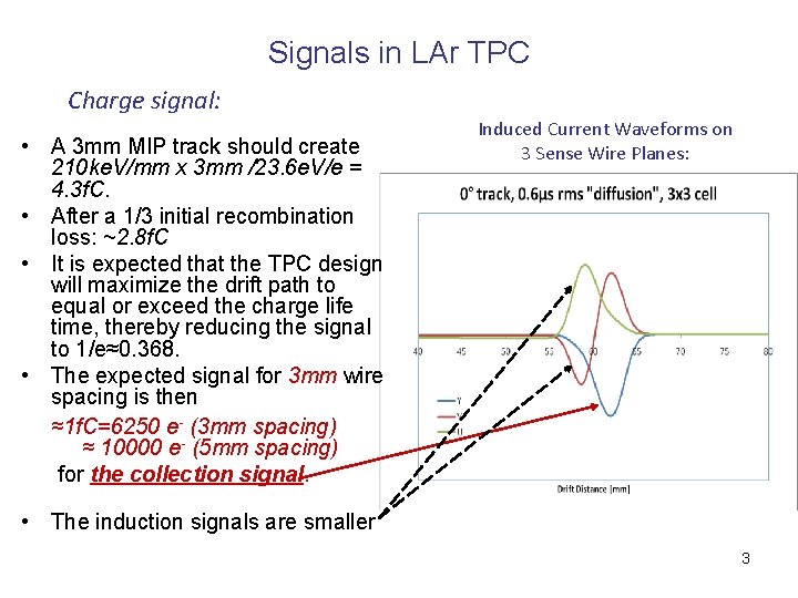
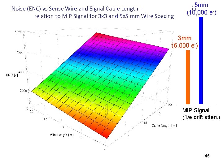
Signals in LAr TPC Charge signal: • A 3 mm MIP track should create 210 ke. V/mm x 3 mm /23. 6 e. V/e = 4. 3 f. C. • After a 1/3 initial recombination loss: ~2. 8 f. C • It is expected that the TPC design will maximize the drift path to equal or exceed the charge life time, thereby reducing the signal to 1/e≈0. 368. • The expected signal for 3 mm wire spacing is then ≈1 f. C=6250 e- (3 mm spacing) ≈ 10000 e- (5 mm spacing) for the collection signal. Induced Current Waveforms on 3 Sense Wire Planes: . • The induction signals are smaller 3

1 Noise mechanisms 4

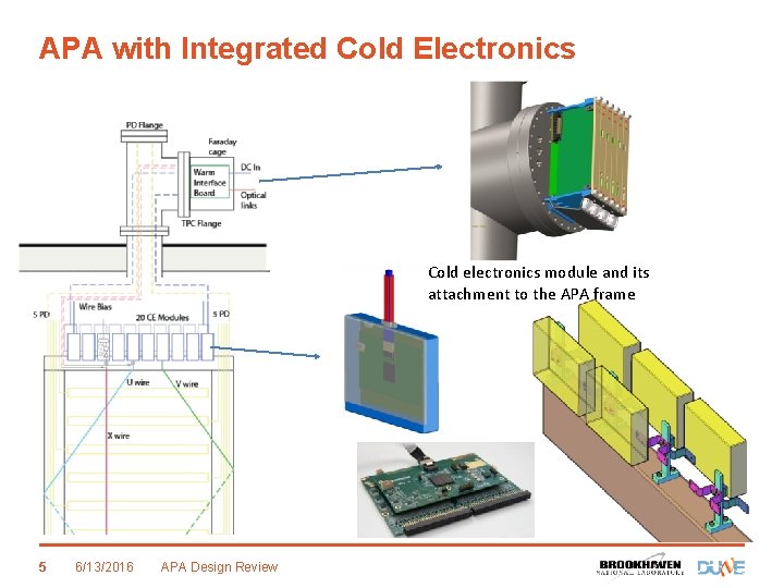
APA with Integrated Cold Electronics Cold electronics module and its attachment to the APA frame 5 6/13/2016 APA Design Review

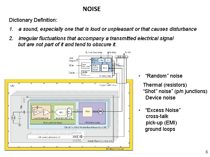
NOISE Dictionary Definition: . 1. a sound, especially one that is loud or unpleasant or that causes disturbance. 2. irregular fluctuations that accompany a transmitted electrical signal but are not part of it and tend to obscure it. • “Random” noise. Thermal (resistors) “Shot” noise” (p/n junctions) Device noise • “Excess Noise” cross-talk pick-up (EMI) ground loops 6

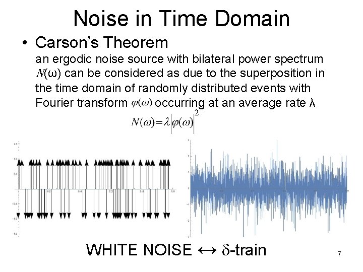
Noise in Time Domain • Carson’s Theorem an ergodic noise source with bilateral power spectrum N(ω) can be considered as due to the superposition in the time domain of randomly distributed events with Fourier transform occurring at an average rate λ WHITE NOISE ↔ d-train 7

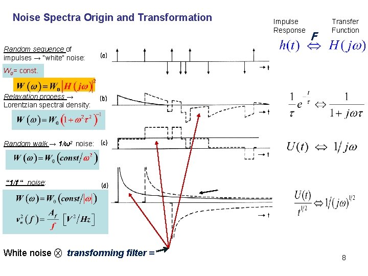
Noise Spectra Origin and Transformation Impulse Response F Transfer Function Random sequence of impulses → “white” noise: W 0= const. Relaxation process → Lorentzian spectral density: Random walk → 1/ω2 noise: “ 1/f “ noise: White noise transforming filter = 8

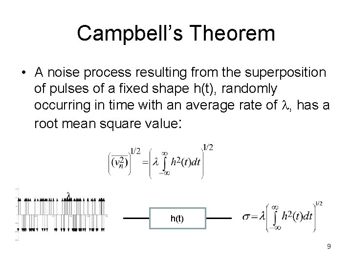
Campbell’s Theorem • A noise process resulting from the superposition of pulses of a fixed shape h(t), randomly occurring in time with an average rate of l, has a root mean square value: l h(t) 9

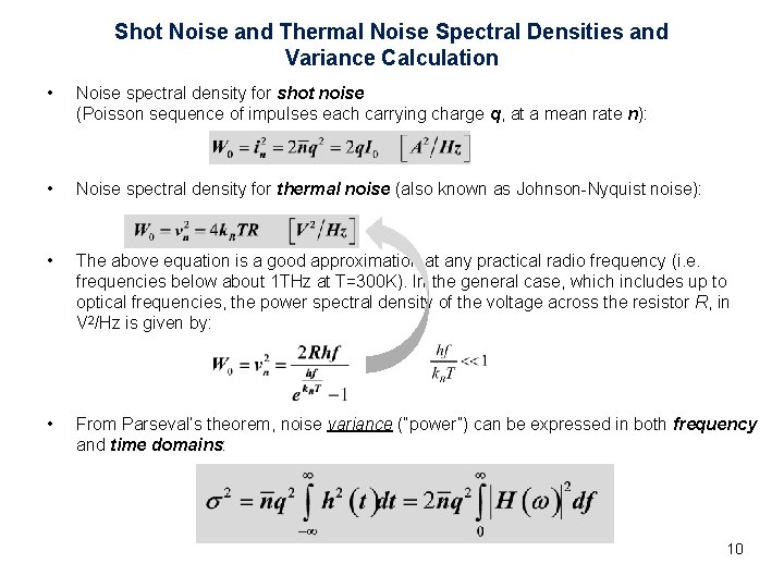
Shot Noise and Thermal Noise Spectral Densities and Variance Calculation • Noise spectral density for shot noise (Poisson sequence of impulses each carrying charge q, at a mean rate n): • Noise spectral density for thermal noise (also known as Johnson-Nyquist noise): • The above equation is a good approximation at any practical radio frequency (i. e. frequencies below about 1 THz at T=300 K). In the general case, which includes up to optical frequencies, the power spectral density of the voltage across the resistor R, in V 2/Hz is given by: • From Parseval’s theorem, noise variance (“power”) can be expressed in both frequency and time domains: 10

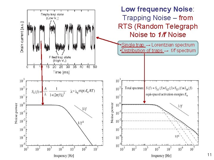
Low frequency Noise: Trapping Noise – from RTS (Random Telegraph Noise to 1/f Noise • Single trap → Lorentzian spectrum • Distribution of traps → 1/f spectrum 11

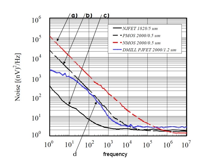
d frequency

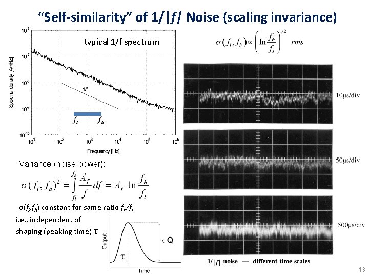
“Self-similarity” of 1/|f| Noise (scaling invariance) typical 1/f spectrum Variance (noise power): σ(fl, fh) constant for same ratio fh/fl i. e. , independent of shaping (peaking time) τ 13

3. Equivalent noise charge (ENC) calculation 14

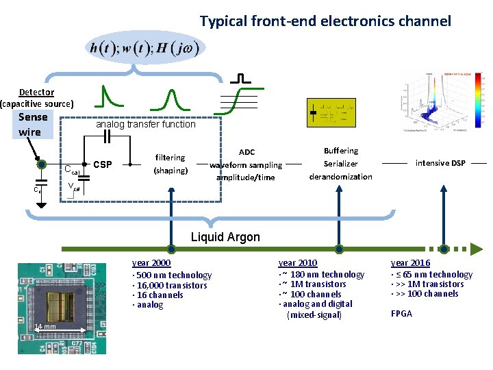
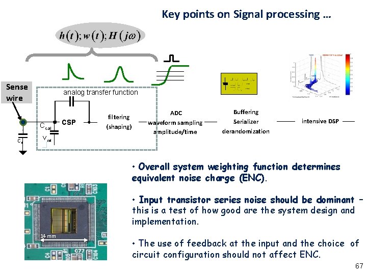
Typical front-end electronics channel Detector (capacitive source) Sense wire analog transfer function Ccal Cd Vcal CSP filtering (shaping) ADC waveform sampling amplitude/time Buffering Serializer derandomization intensive DSP Liquid Argon year 2000 · 500 nm technology · 16, 000 transistors · 16 channels · analog 14 mm year 2010 · ~ 180 nm technology · ~ 1 M transistors · ~ 100 channels · analog and digital (mixed-signal) year 2016 · ≤ 65 nm technology · >> 1 M transistors · >> 100 channels FPGA

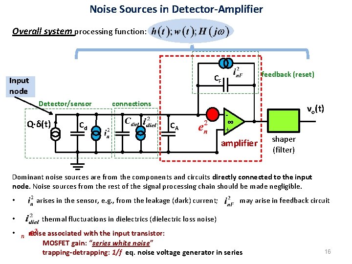
Noise Sources in Detector-Amplifier Overall system processing function: feedback (reset) CF Input node Detector/sensor Q·δ(t) Cd connections CA vo(t) ∞ + amplifier shaper (filter) Dominant noise sources are from the components and circuits directly connected to the input node. Noise sources from the rest of the signal processing chain should be made negligible. • arises in the sensor, e. g. , from the leakage (dark) current; may arise in feedback circuit • thermal fluctuations in dielectrics (dielectric loss noise) • n noise e 2 associated with the input transistor: MOSFET gain: “series white noise” trapping-detrapping: 1/f eq. noise voltage generator in series 16

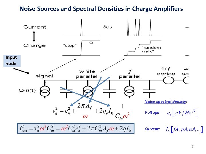
Noise Sources and Spectral Densities in Charge Amplifiers Input node Noise spectral density: Voltage: Current: 17

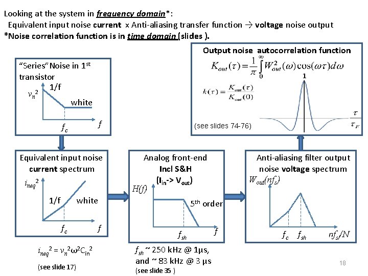
Looking at the system in frequency domain*: Equivalent input noise current x Anti-aliasing transfer function → voltage noise output *Noise correlation function is in time domain (slides ). Output noise autocorrelation function “Series”Noise in 1 st transistor 1/f vn 2 white 1 f fc Equivalent input noise current spectrum ineq 2 1/f (see slides 74 -76) Analog front-end Incl S&H (Iin-> Vout) H(f) white fc ineq 2 = vn 2ω2 Cin 2 (see slide 17) Anti-aliasing filter output noise voltage spectrum Wout(nfs) 5 th order f fsh ~ 250 k. Hz @ 1µs, and ~ 83 k. Hz @ 3 µs (see slide 35 ) fc fsh nfs//N 18

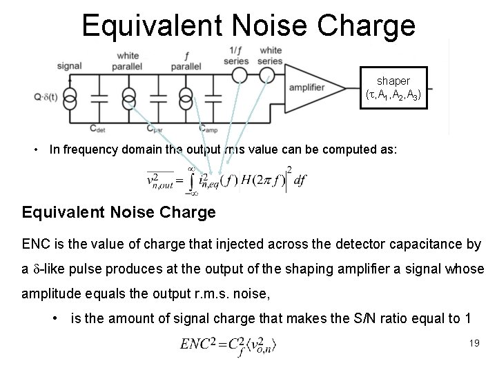
Equivalent Noise Charge shaper (t, A 1, A 2, A 3) • In frequency domain the output rms value can be computed as: Equivalent Noise Charge. ENC is the value of charge that injected across the detector capacitance by a d-like pulse produces at the output of the shaping amplifier a signal whose amplitude equals the output r. m. s. noise, • is the amount of signal charge that makes the S/N ratio equal to 1 19

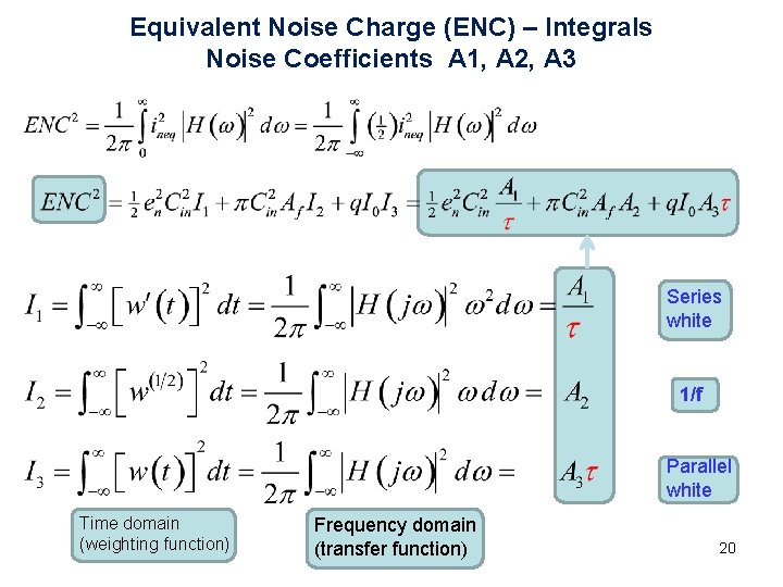
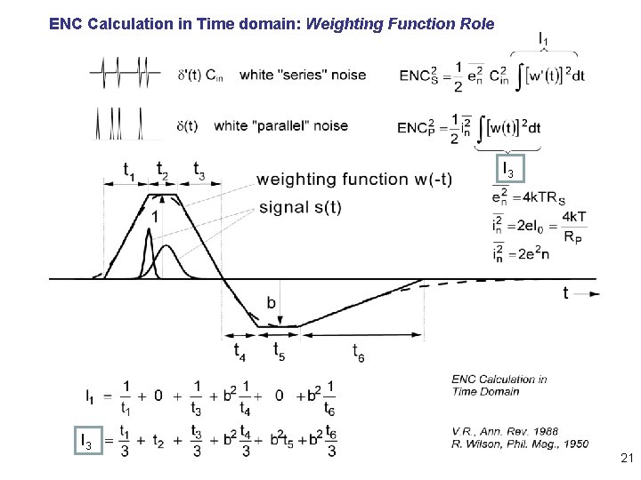
Equivalent Noise Charge (ENC) – Integrals Noise Coefficients A 1, A 2, A 3 Series white 1/f Parallel white Time domain (weighting function) Frequency domain (transfer function) 20

ENC Calculation in Time domain: Weighting Function Role I 3 21

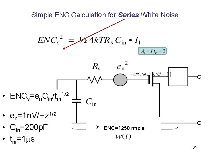
Simple ENC Calculation for Series White Noise • ENCs=en. Cin/tm 1/2 • en=1 n. V/Hz 1/2 • Cin=200 p. F • tm=1 ms → ENC=1250 rms e - 22

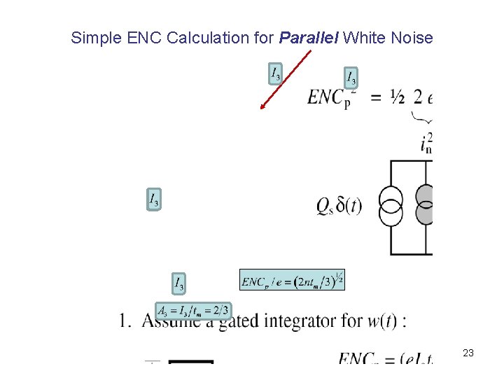
Simple ENC Calculation for Parallel White Noise 23

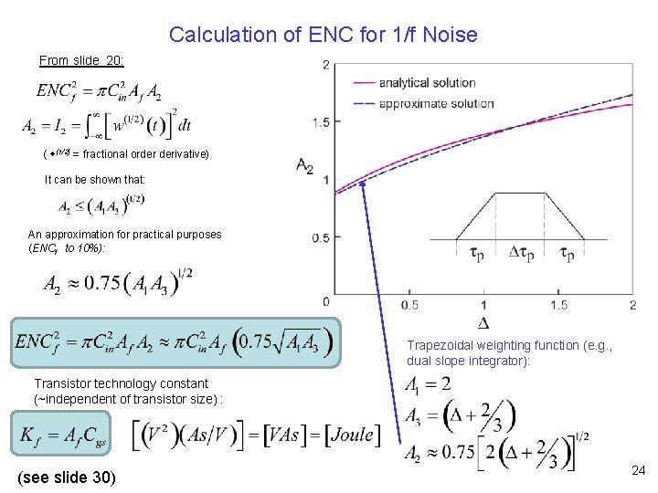
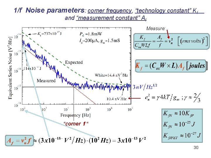
Calculation of ENC for 1/f Noise From slide 20: ( w(1/2) = fractional order derivative) It can be shown that: An approximation for practical purposes (ENCf to 10%): Trapezoidal weighting function (e. g. , dual slope integrator): Transistor technology constant (~independent of transistor size) : (see slide 30) 24

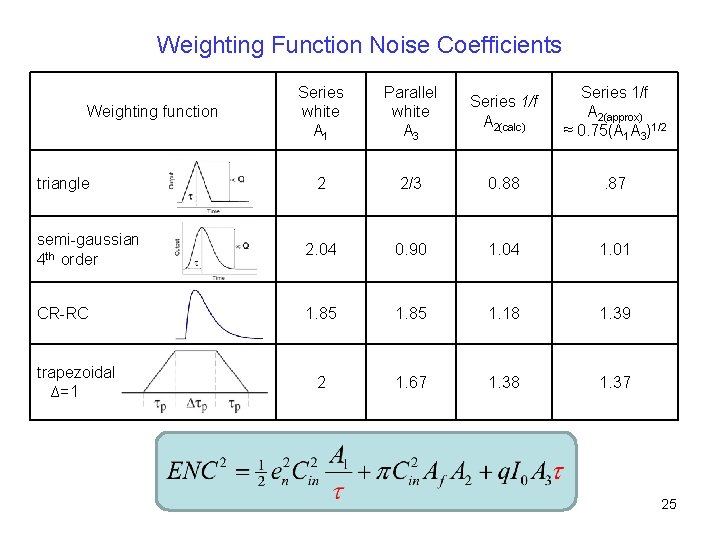
Weighting Function Noise Coefficients Series white A 1 Parallel white A 3 Series 1/f A 2(calc) Series 1/f A 2(approx) ≈ 0. 75(A 1 A 3)1/2 2 2/3 0. 88 . 87 semi-gaussian 4 th order 2. 04 0. 90 1. 04 1. 01 CR-RC 1. 85 1. 18 1. 39 2 1. 67 1. 38 1. 37 Weighting function triangle trapezoidal ∆=1 25

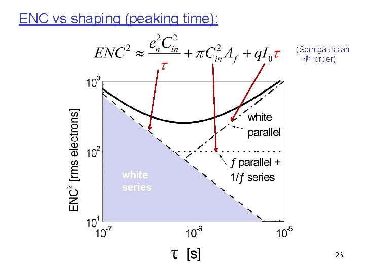
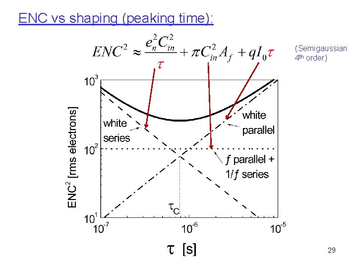
ENC vs shaping (peaking time): (Semigaussian 4 th order) white series 26

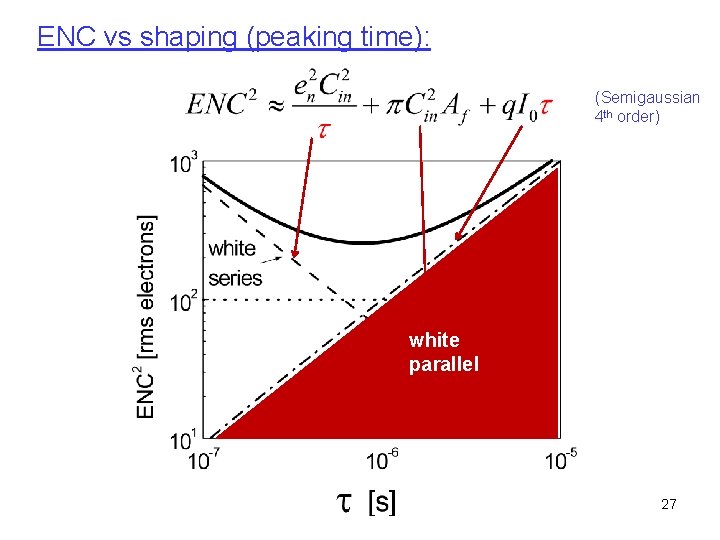
ENC vs shaping (peaking time): (Semigaussian 4 th order) white parallel 27

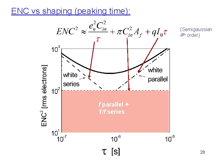
ENC vs shaping (peaking time): (Semigaussian 4 th order) f parallel + 1/f series 28

ENC vs shaping (peaking time): (Semigaussian 4 th order) 29

1/f Noise parameters: corner frequency, “technology constant” Kf and “measurement constant” Af Measure: “corner f “ 30

4. Signal processing, i. e. , “filtering” or “pulse shaping” 31

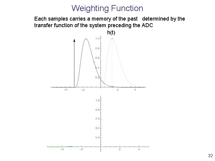
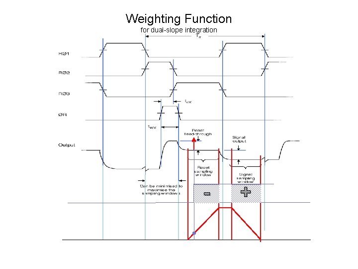
Weighting Function Each samples carries a memory of the past determined by the transfer function of the system preceding the ADC h(t) 32

Weighting Function for dual-slope integration - +

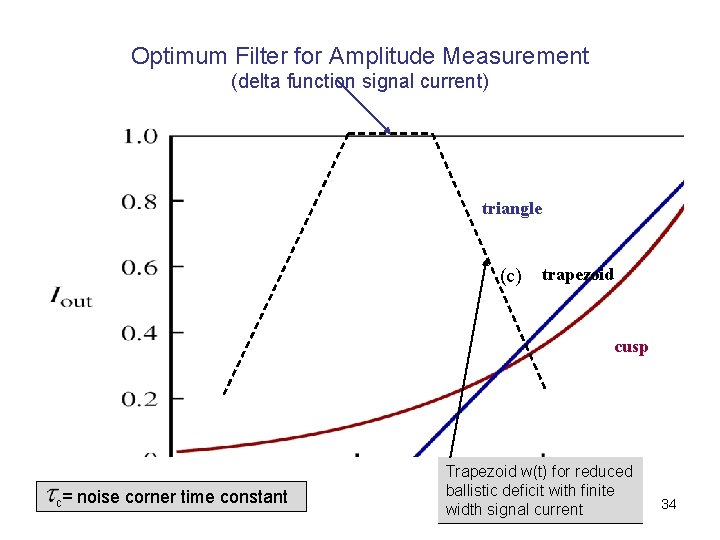
Optimum Filter for Amplitude Measurement (delta function signal current) triangle (c) trapezoid cusp c= noise corner time constant Trapezoid w(t) for reduced ballistic deficit with finite width signal current 34

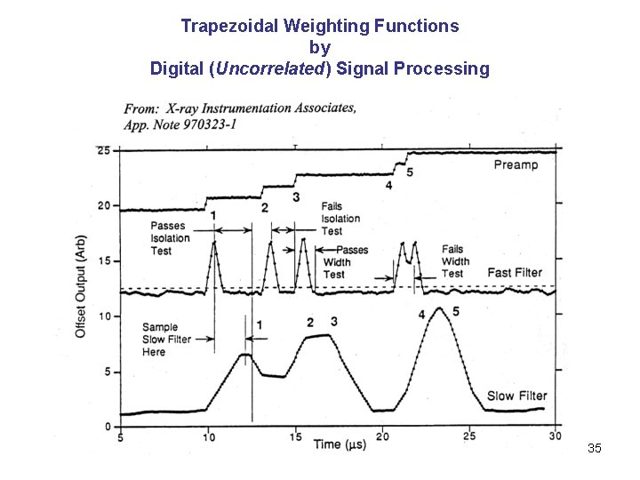
Trapezoidal Weighting Functions by Digital (Uncorrelated) Signal Processing 35

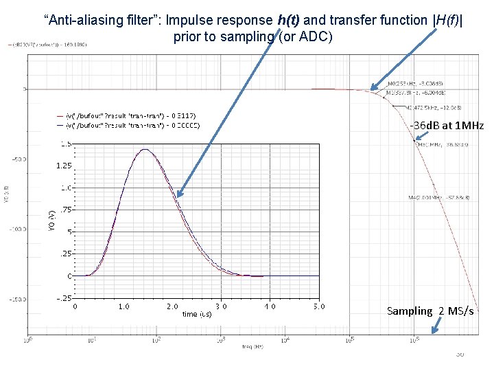
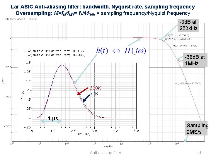
“Anti-aliasing filter”: Impulse response h(t) and transfer function |H(f)| prior to sampling (or ADC) -36 d. B at 1 MHz 1 μs Sampling 2 MS/s 36

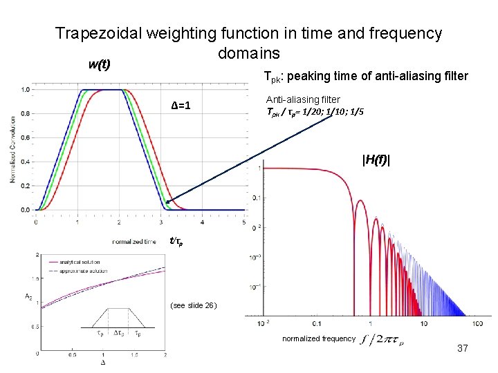
Trapezoidal weighting function in time and frequency domains w(t) Tpk: peaking time of anti-aliasing filter ∆=1 Anti-aliasing filter Tpk / τp= 1/20; 1/10; 1/5 |H(f)| t/τp (see slide 26) normalized frequency 37

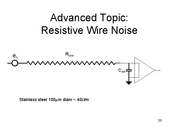
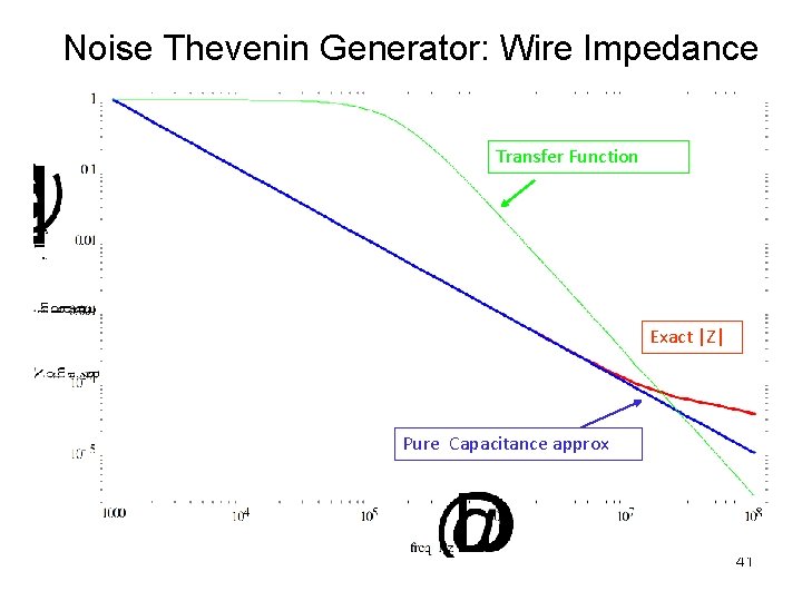
Advanced Topic: Resistive Wire Noise en Rwire Cdet Stainless steel 100μm diam ~ 40Ω/m 38

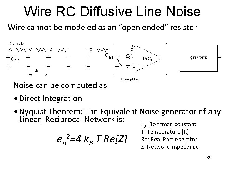
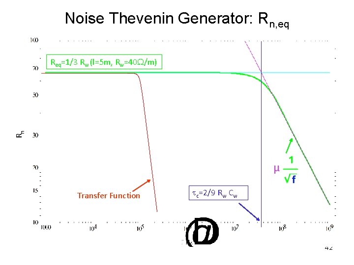
Wire RC Diffusive Line Noise Wire cannot be modeled as an “open ended” resistor Ctot Noise can be computed as: • Direct Integration • Nyquist Theorem: The Equivalent Noise generator of any Linear, Reciprocal Network is: k : Boltzman constant B en 2=4 k. B T Re[Z] T: Temperature [K] Re: Real Part operator Z: Network Impedance 39

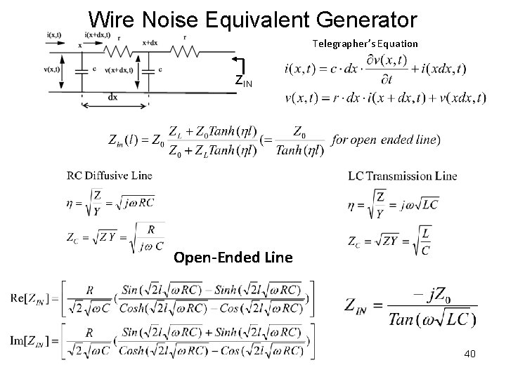
Wire Noise Equivalent Generator Telegrapher’s Equation ZIN Open-Ended Line 40

Noise Thevenin Generator: Wire Impedance Transfer Function Exact |Z| Pure Capacitance approx 41

Noise Thevenin Generator: Rn, eq Rn Req=1/3 Rw (l=5 m, Rw=40 W/m) Transfer Function tc=2/9 Rw Cw 42

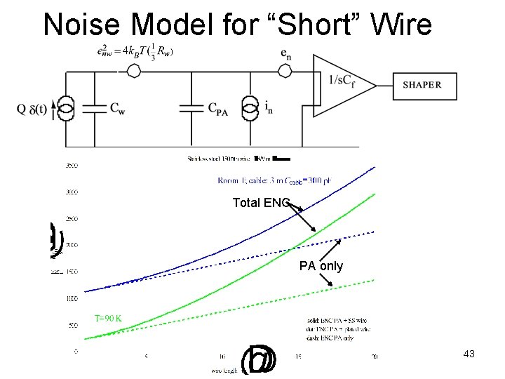
Noise Model for “Short” Wire Total ENC PA only 43

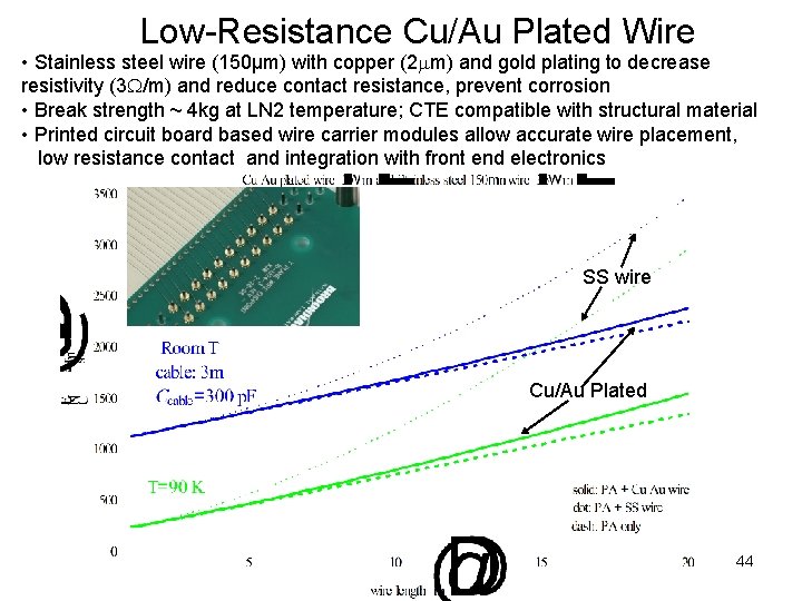
Low-Resistance Cu/Au Plated Wire • Stainless steel wire (150µm) with copper (2 mm) and gold plating to decrease resistivity (3 W/m) and reduce contact resistance, prevent corrosion • Break strength ~ 4 kg at LN 2 temperature; CTE compatible with structural material • Printed circuit board based wire carrier modules allow accurate wire placement, low resistance contact and integration with front end electronics SS wire Cu/Au Plated 44

5 mm Noise (ENC) vs Sense Wire and Signal Cable Length - in (10, 000 e-) relation to MIP Signal for 3 x 3 and 5 x 5 mm Wire Spacing 3 mm (6, 000 e-) MIP Signal (1/e drift atten. ) 45

Conclusions: • Low noise TPC readout requires reduction of wire resistance noise (and capacitance!) • Simple model can be used for wire lengths of up to ~20 m (for Cw~20 p. F/m, tm~1 ms) • Req, wire=1/3 Rw, “loaded” by Cw • Wire plating reduces Rw to ~3 W/m • Limiting C (wire, connection) essential to achieve low noise 46

Anti-aliasing Filters for TPC Current Waveform Sampling Anti-aliasing filter 47

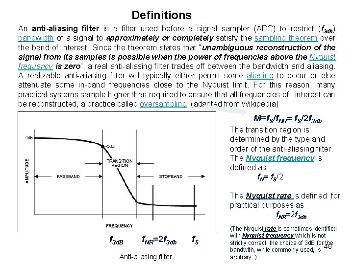
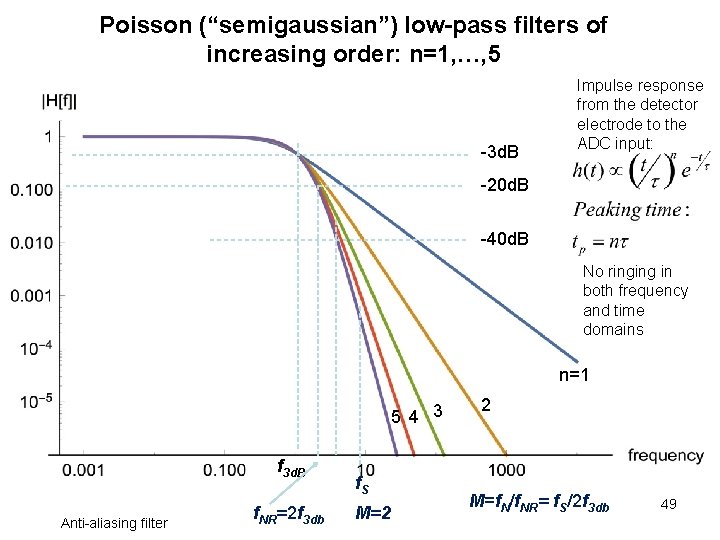
Definitions An anti-aliasing filter is a filter used before a signal sampler (ADC) to restrict (f 3 db) bandwidth of a signal to approximately or completely satisfy the sampling theorem over the band of interest. Since theorem states that “unambiguous reconstruction of the signal from its samples is possible when the power of frequencies above the Nyquist frequency is zero”, a real anti-aliasing filter trades off between the bandwidth and aliasing. A realizable anti-aliasing filter will typically either permit some aliasing to occur or else attenuate some in-band frequencies close to the Nyquist limit. For this reason, many practical systems sample higher than required to ensure that all frequencies of interest can be reconstructed, a practice called oversampling (adapted from Wikipedia) M=f. S/f. NR= f. S/2 f 3 db The transition region is determined by the type and order of the anti-aliasing filter. The Nyquist frequency is defined as f. N= f. S/2 The Nyquist rate is defined for practical purposes as f. NR=2 f 3 db f 3 d. B f. NR=2 f 3 db Anti-aliasing filter f. S (The Nyquist rate is sometimes identified with Nyquist frequency which is not strictly correct; the choice of 3 d. B for the 48 bandwith, while commonly used, is arbitrary. )

Poisson (“semigaussian”) low-pass filters of increasing order: n=1, …, 5 -3 d. B Impulse response from the detector electrode to the ADC input: -20 d. B -40 d. B No ringing in both frequency and time domains n=1 5 4 3 f 3 d. B Anti-aliasing filter f. NR=2 f 3 db f. S M=2 2 M=f. N/f. NR= f. S/2 f 3 db 49

Lar ASIC Anti-aliasing filter: bandwidth, Nyquist rate, sampling frequency Oversampling: M=f. N/f. NR= f. S/4 f 3 db = sampling frequency/Nyquist frequency -3 d. B at 253 k. Hz -36 d. B at 1 MHz 300 K 77 K 1 μs Sampling 2 MS/s Anti-aliasing filter 50

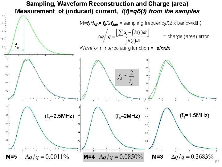
Sampling, Waveform Reconstruction and Charge (area) Measurement of (induced) current, i(t)=qδ(t) from the samples M=f. S/f. NR= f. S/2 f 3 db = sampling frequency/(2 x bandwidth) . = charge (area) error tp Waveform interpolating function = sinx/x (fs=2. 5 MHz) M=5 (fs=1. 5 MHz) (fs=2 MHz) M=4 M=3 51

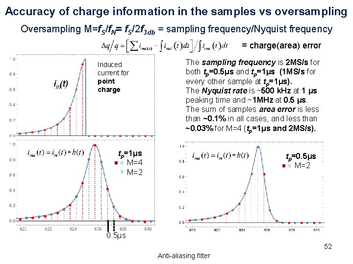
Accuracy of charge information in the samples vs oversampling Oversampling M=f. S/f. N= f. S/2 f 3 db = sampling frequency/Nyquist frequency = charge(area) error iin(t) Induced current for point charge The sampling frequency is 2 MS/s for both tp=0. 5μs and tp=1μs (1 MS/s for every other sample at tp=1μs). The Nyquist rate is ~500 k. Hz at 1 μs peaking time and ~1 MHz at 0. 5 μs. The sum of samples area error is less than ~0. 1% in all cases, and less than ~0. 03% for M=4 (tp=1μs and 2 MS/s). tp=1μs M=4 M=2 tp=0. 5μs M=2 0. 5µs 52 Anti-aliasing filter

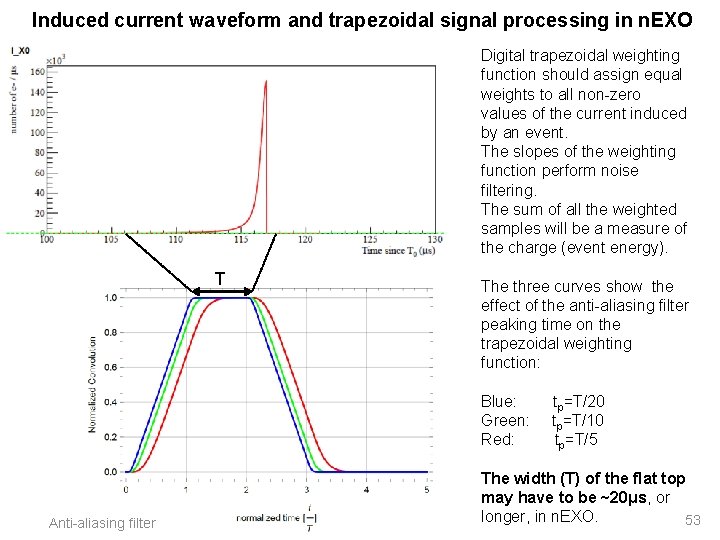
Induced current waveform and trapezoidal signal processing in n. EXO Digital trapezoidal weighting function should assign equal weights to all non-zero values of the current induced by an event. The slopes of the weighting function perform noise filtering. The sum of all the weighted samples will be a measure of the charge (event energy). T The three curves show the effect of the anti-aliasing filter peaking time on the trapezoidal weighting function: Blue: tp=T/20 Green: tp=T/10 Red: tp=T/5 Anti-aliasing filter The width (T) of the flat top may have to be ~20μs, or longer, in n. EXO. 53

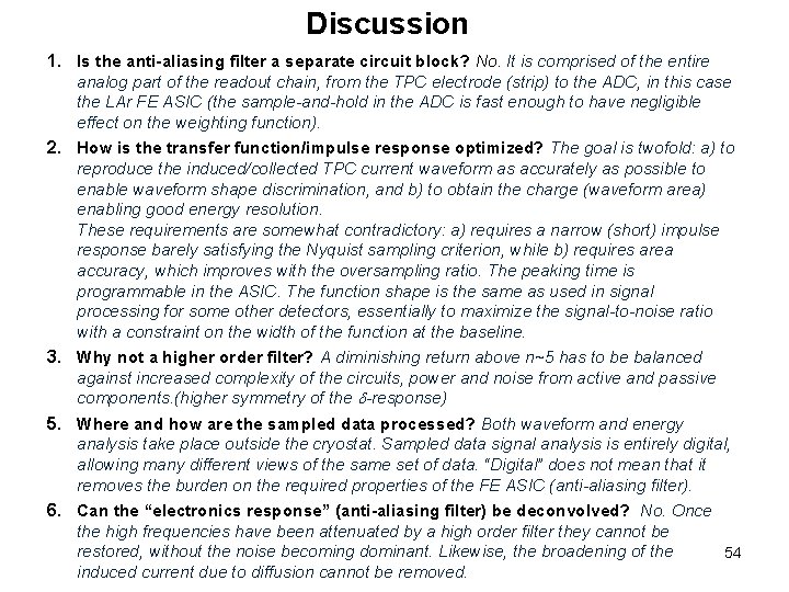
Discussion 1. Is the anti-aliasing filter a separate circuit block? No. It is comprised of the entire analog part of the readout chain, from the TPC electrode (strip) to the ADC, in this case the LAr FE ASIC (the sample-and-hold in the ADC is fast enough to have negligible effect on the weighting function). 2. How is the transfer function/impulse response optimized? The goal is twofold: a) to reproduce the induced/collected TPC current waveform as accurately as possible to enable waveform shape discrimination, and b) to obtain the charge (waveform area) enabling good energy resolution. These requirements are somewhat contradictory: a) requires a narrow (short) impulse response barely satisfying the Nyquist sampling criterion, while b) requires area accuracy, which improves with the oversampling ratio. The peaking time is programmable in the ASIC. The function shape is the same as used in signal processing for some other detectors, essentially to maximize the signal-to-noise ratio with a constraint on the width of the function at the baseline. 3. Why not a higher order filter? A diminishing return above n~5 has to be balanced against increased complexity of the circuits, power and noise from active and passive components. (higher symmetry of the d-response) 5. Where and how are the sampled data processed? Both waveform and energy analysis take place outside the cryostat. Sampled data signal analysis is entirely digital, allowing many different views of the same set of data. “Digital” does not mean that it removes the burden on the required properties of the FE ASIC (anti-aliasing filter). 6. Can the “electronics response” (anti-aliasing filter) be deconvolved? No. Once the high frequencies have been attenuated by a high order filter they cannot be restored, without the noise becoming dominant. Likewise, the broadening of the 54 induced current due to diffusion cannot be removed. . . 4. .

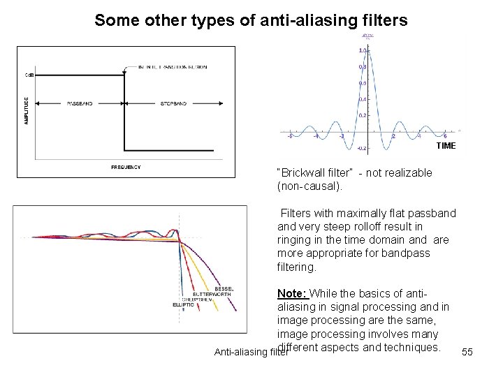
Some other types of anti-aliasing filters TIME “Brickwall filter” - not realizable (non-causal). Filters with maximally flat passband very steep rolloff result in ringing in the time domain and are more appropriate for bandpass filtering. Note: While the basics of antialiasing in signal processing and in image processing are the same, image processing involves many different aspects and techniques. Anti-aliasing filter 55

Noise from Dielectrics 56

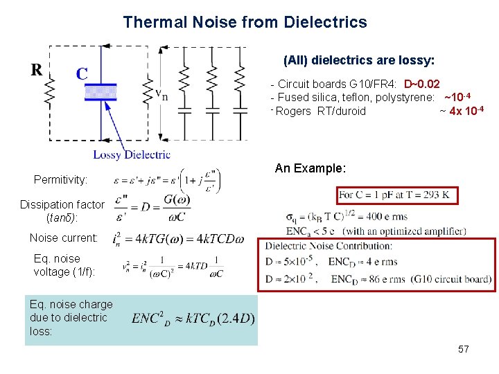
Thermal Noise from Dielectrics (All) dielectrics are lossy: - Circuit boards G 10/FR 4: D~0. 02 - Fused silica, teflon, polystyrene: ~10 -4 - Rogers RT/duroid ~ 4 x 10 -4 Permitivity: An Example: Dissipation factor (tanδ): Noise current: Eq. noise voltage (1/f): Eq. noise charge due to dielectric loss: 57

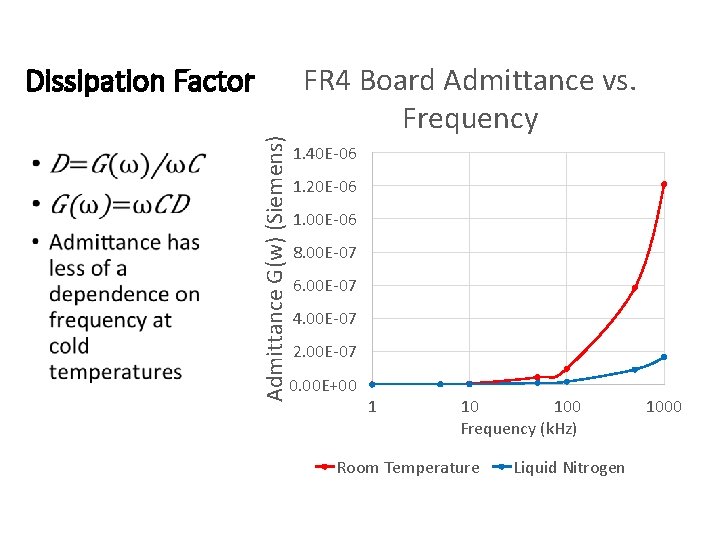
• Admittance G(w) (Siemens) Dissipation Factor FR 4 Board Admittance vs. Frequency 1. 40 E-06 1. 20 E-06 1. 00 E-06 8. 00 E-07 6. 00 E-07 4. 00 E-07 2. 00 E-07 0. 00 E+00 1 10 100 Frequency (k. Hz) Room Temperature Liquid Nitrogen 1000

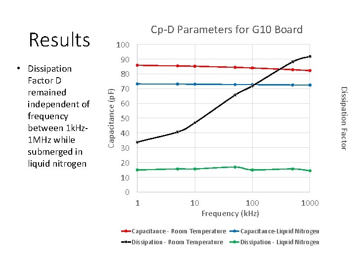
Results Capacitance (p. F) Dissipation Factor Frequency (k. Hz)

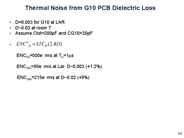
Thermal Noise from G 10 PCB Dielectric Loss • D=0. 003 for G 10 at LAR • D~0. 02 at room T • Assume Ctot=200 p. F and CG 10=20 p. F • . ENCtot=500 e- rms at Tp=1μs ENCdiel=80 e- rms at Lar D~0. 003 (+1. 2%) ENCdiel=215 e- rms at D~0. 02 (+9%) 60

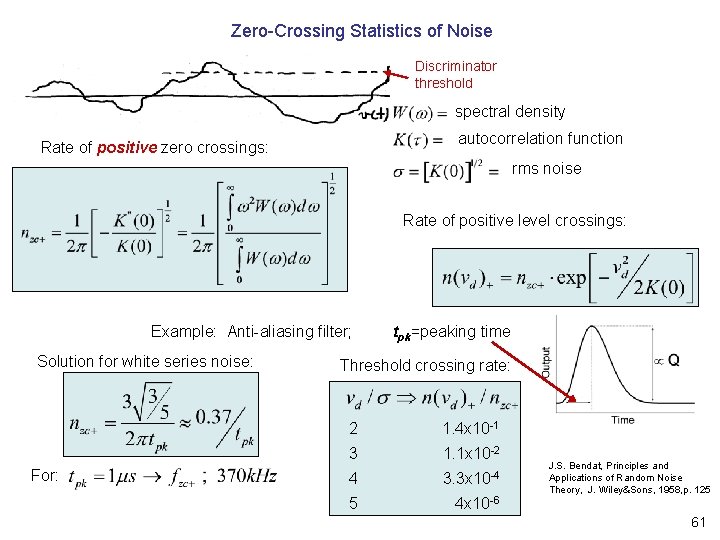
Zero-Crossing Statistics of Noise Discriminator threshold spectral density autocorrelation function Rate of positive zero crossings: rms noise Rate of positive level crossings: Example: Anti-aliasing filter; tpk=peaking time Solution for white series noise: Threshold crossing rate: 2 1. 4 x 10 -1 For: 3 1. 1 x 10 -2 4 3. 3 x 10 -4 5 4 x 10 -6 J. S. Bendat, Principles and Applications of Random Noise Theory, J. Wiley&Sons, 1958, p. 125 61

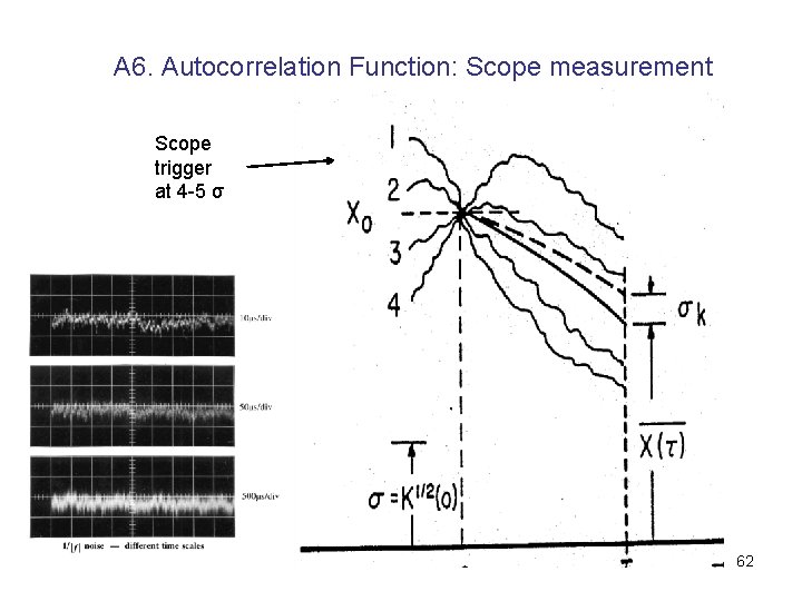
A 6. Autocorrelation Function: Scope measurement Scope trigger at 4 -5 σ 62

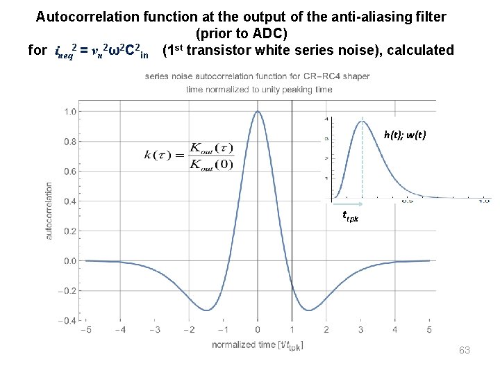
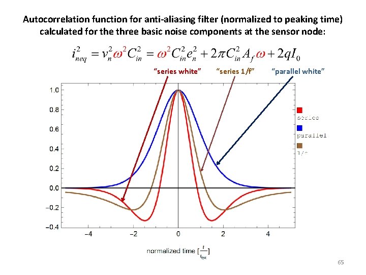
Autocorrelation function at the output of the anti-aliasing filter (prior to ADC) for ineq 2 = vn 2ω2 C 2 in (1 st transistor white series noise), calculated → t h(t); w(t) ttpk 63

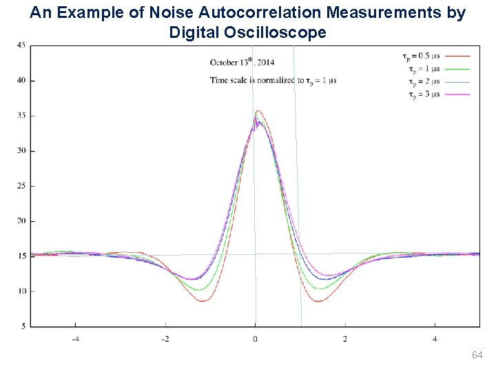
An Example of Noise Autocorrelation Measurements by Digital Oscilloscope 64

Autocorrelation function for anti-aliasing filter (normalized to peaking time) calculated for the three basic noise components at the sensor node: “series white” “series 1/f” “parallel white” 65

8. Concluding Remarks 66

Key points on Signal processing … Sense wire analog transfer function Ccal Cd Vcal CSP filtering (shaping) ADC waveform sampling amplitude/time Buffering Serializer derandomization intensive DSP • Overall system weighting function determines equivalent noise charge (ENC). • Input transistor series noise should be dominant – this is a test of how good are the system design and implementation. 14 mm • The use of feedback at the input and the choice of circuit configuration should not affect ENC. 67

9. Literature 68

REFERENCES ON SIGNAL PROCESSING FOR RADIATION DETECTORS 1. S. Ramo; Proc. IRE, 27(1939) 584. 2. E. Gatti, G. Padovini, and V. Radeka; Signal Evaluation in Multielectrode Radiation Detectors by Means of a Time Dependent Weighting Vector; NIM 193 (1982) 651. 3. R. Wilson; Noise in Ionization Chamber Pulse Amplifiers; Philosophical Magazine, Ser. 7, Vol. xli, p. 66, Jan. (1950). 4. E. Baldinger and W. Franzen; Advances in Electronics and Electron Physics; 3 Academic Press, New York, (1956) 256. 5. V. Radeka; Optimum Signal Processing for Pulse Amplitude Spectrometry in the Presence of High-Rate Effects and Noise; IEEE Trans. Nucl. Sci. NS-15 (1968) 455. 6. M. Konrad; Detector Pulse Shaping for High Resolution Spectroscopy; IEEE Trans. Nucl. Sci. NS-15, No. 1 (1968) 268. 7. V. Radeka; State of the Art of Low Noise Amplifiers for Semiconductor Radiation Detectors; Proc. Int’l. Symposium on Nuclear Electronics, Versailles, 1968, Vol. 1 : 1 (1968). 8. V. Radeka; Field Effect Transistors for Charge Amplifiers; IEEE Trans. Nucl. Sci. NS-20, 182 (1973). 9. V. Radeka; Trapezoidal Filtering of Signals from Large Germanium Detectors at High Rates; Nucl. Instrum. & Meth. 99 (1972) 535. 10. V. Radeka; 1/| f | Noise in Physical Measurements; IEEE Trans. Nucl. Sci. NS-16 (1969) 17. 11. V. Radeka; Signal, Noise, and Resolution in Position-Sensitive Detectors; IEEE Trans. Nucl. Sci. NS-21, No. 1 (1974) 51. 12. W. J. Willis and V. Radeka; Liquid Argon Ionization Chambers as Total Absorption Detectors; Nucl. Instrum. & Meth. 120 (1974) 221. 13. V. Radeka and R. A. Boie; Centroid Finding Method for Position Sensitive Detectors; Nucl. Instrum. & Meth. 178 (1980) 543. 14. F. S. Goulding, D. A. Landis, and N. W. Madden; IEEE Trans. Nucl. Sci. NS-30, 301 (1983). 15. V. Radeka; Semiconductor Position Sensitive Detectors; NIM 226 (1984) 209. 69

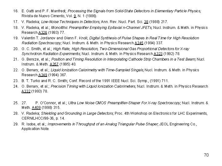
16. E. Gatti and P. F. Manfredi; Processing the Signals from Solid-State Detectors in Elementary Particle Physics; Rivista de Nuovo Cimento, Vol. 9, N. 1 (1986). 17. V. Radeka; Low-Noise Techniques in Detectors; Ann. Rev. Nucl. Part. Sci. 38 (1988) 217. 18. V. Radeka, et al. ; Monolithic Preamplifier Employing Epitaxial n-Channel JFETs; Nucl. Instrum. & Meth. in Physics Research A 326 (1993) 77. 19. Valentin T. Jordanov and Glenn F. Knoll; Digital Synthesis of Pulse Shapes in Real Time for High Resolution Radiation Spectroscopy; Nucl. Instrum. & Meth. in Physics Research A 345 (1994) 337. 20. G. C. Smith, et al. ; High Rate, High Resolution, Two-Dimensional Gas Proportional Detectors for X-ray Synchrotron Radiation Experiments; Nucl. Instrum. & Meth. in Physics Research A 323 (1992) 78. 21. G. Bencze, et al. ; Position and Timing Resolution in Interpolating Cathode Strip Chambers in a Test Beam; Nucl. Instrum. & Meth. A 357 (1995) 40. 22. O. Benary, et al. ; Liquid Ionization Calorimetry with Time-Sampled Singals; Nucl. Instrum. & Meth. in Physics Research A 349 (1994) 367. 23. B. T. Turko and R. C. Smith; Conf. Record of the 1991 IEEE Nucl. Sci. Symp. , (1991) 711. 24. O. Benary, et al. ; Precision Timing with Liquid Ionization Calorimeters; Nucl. Instrum. & Meth. in Physics Research A 332 (1993) 78. 25. 27. P. O’Connor, et al. ; Ultra Low Noise CMOS Preamplifier-Shaper For X-ray Spectroscopy; Nucl. Instrum. & Meth. A 409 (1998) 315. 28. V. Radeka; Shielding and Grounding in Large Detectors; Proc. 4 th Workshop on Electronics for LHC Experiments, CERN/LHCC/98 -36, p. 14. 29. R. Isobe, et al. ; Improvements in Throughput of an Analog Triangular Pulse Shaper; JEOL Engineering Co. , Application Note. 70

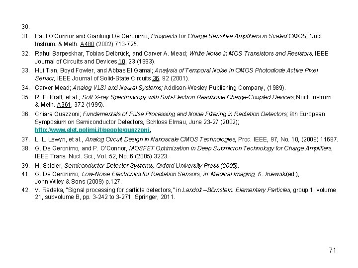
30. 31. Paul O’Connor and Gianluigi De Geronimo; Prospects for Charge Sensitive Amplifiers in Scaled CMOS; Nucl. Instrum. & Meth. A 480 (2002) 713 -725. 32. Rahul Sarpeskhar, Tobias Delbrück, and Carver A. Mead; White Noise in MOS Transistors and Resistors; IEEE Journal of Circuits and Devices 10, 23 (1993). 33. Hui Tian, Boyd Fowler, and Abbas El Gamal; Analysis of Temporal Noise in CMOS Photodiode Active Pixel Sensor; IEEE Journal of Solid-State Circuits 36, 92 (2001). 34. Carver Mead; Analog VLSI and Neural Systems; Addison-Wesley Publishing Company, (1989). 35. R. P. Kraft, et al. ; Soft X-ray Spectroscopy with Sub-Electron Readnoise Charge-Coupled Devices; Nucl. Instrum. & Meth. A 361, 372 (1995). 36. Chiara Guazzoni; Fundamentals of Pulse Processing and Noise Filtering in Radiation Detectors; 9 th European Symposium on Semiconductor Detectors, Schloss Elmau, June 23 -27 (2002); http: //www. elet. polimi. it/people/guazzoni. 37. L. L. Lewyn, et al. , Analog Circuit Design in Nanoscale CMOS Technologies, Proc. IEEE, 97, No. 10, (2009) 11687. 38. G. De Geronimo, and P. O’Connor, MOSFET Optimization in Deep Submicron Technology for Charge Amplifiers, IEEE Trans. Nucl. Sci. , Vol. 52, No. 6 (2005) 3223. 39. H. Spieler, Semiconductor Detector Systems, Oxford University Press (2005). 41. G. De Geronimo, Low-Noise Electronics for Radiation Sensors, in: Medical Imaging, K. Iniewski(ed. ), John Wiley & Sons (2009) p. 127. 42. V. Radeka, “Signal processing for particle detectors, ” in Landolt –Börnstein: Elementary Particles, group 1, volume 21, subvolume B, pp. 3 -242 to 3 -271, Springer, 2011. 71

Appendix 72

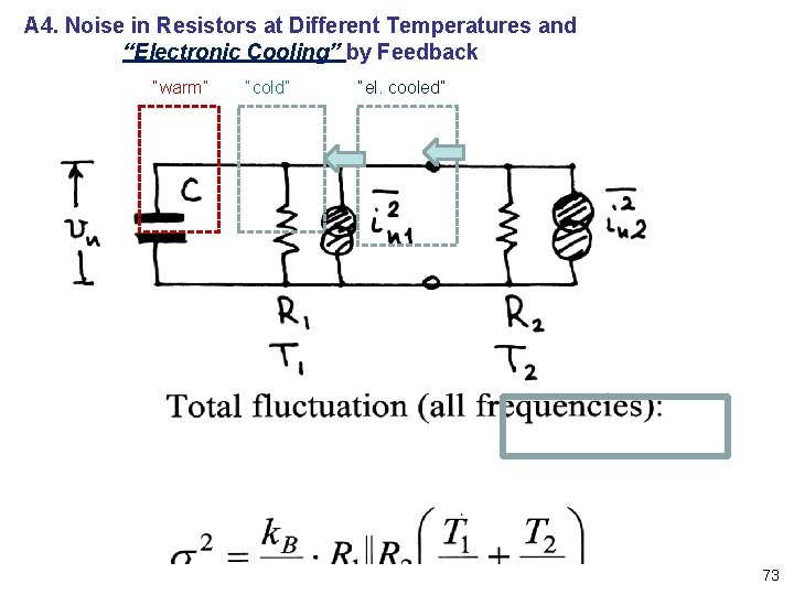
A 4. Noise in Resistors at Different Temperatures and “Electronic Cooling” by Feedback “warm” “cold” “el. cooled” 73