Design and Implementation of VLSI Systems EN 0160


- Slides: 25

Design and Implementation of VLSI Systems (EN 0160) Lecture 34: Design Methods (beyond Tanner Tools) Prof. Sherief Reda Division of Engineering, Brown University Spring 2007 [sources: Weste/Addison Wesley – Maxfield/Newnes] S. Reda EN 160 SP’ 07

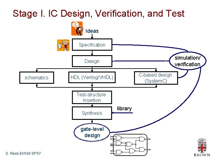
Stage I. IC Design, Verification, and Test Ideas Specification simulation/ verification Design schematics C-based design (System. C) HDL (Verilog/VHDL) Test-structure Insertion Synthesis gate-level design S. Reda EN 160 SP’ 07 library

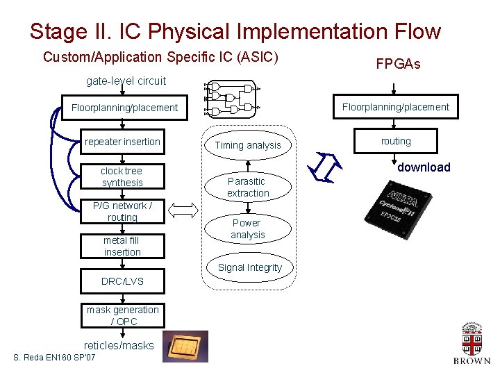
Stage II. IC Physical Implementation Flow Custom/Application Specific IC (ASIC) FPGAs gate-level circuit Floorplanning/placement repeater insertion clock tree synthesis P/G network / routing metal fill insertion Timing analysis download Parasitic extraction Power analysis Signal Integrity DRC/LVS mask generation / OPC reticles/masks S. Reda EN 160 SP’ 07 routing

Stage III. Fabrication and Packaging reticles fabricate wafer Test dies dice and package the good ones chips S. Reda EN 160 SP’ 07

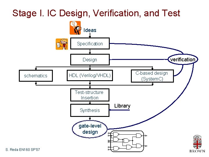
Stage I. IC Design, Verification, and Test Ideas Specification verification Design schematics C-based design (System. C) HDL (Verilog/VHDL) Test-structure Insertion Synthesis gate-level design S. Reda EN 160 SP’ 07 Library

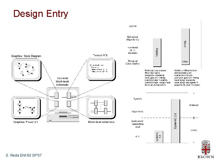
Design Entry S. Reda EN 160 SP’ 07

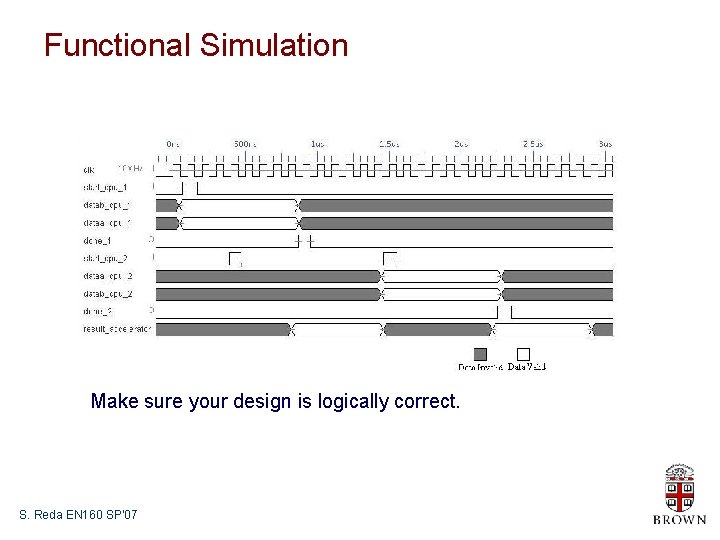
Functional Simulation Make sure your design is logically correct. S. Reda EN 160 SP’ 07

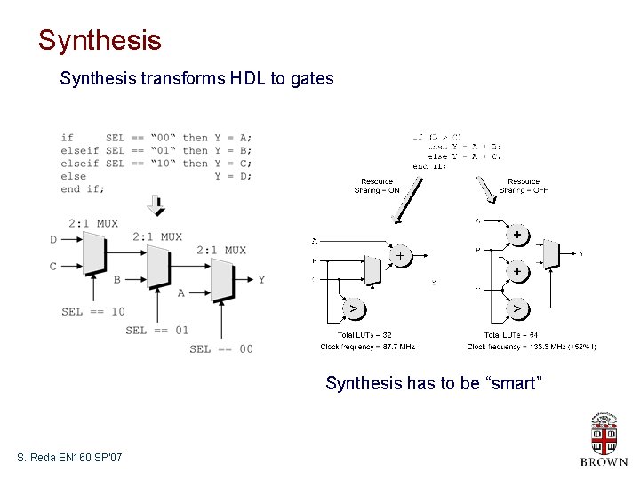
Synthesis transforms HDL to gates Synthesis has to be “smart” S. Reda EN 160 SP’ 07

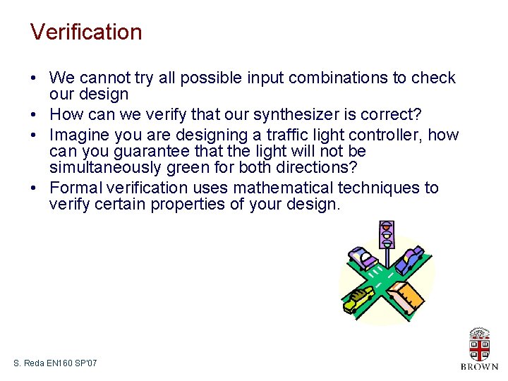
Verification • We cannot try all possible input combinations to check our design • How can we verify that our synthesizer is correct? • Imagine you are designing a traffic light controller, how can you guarantee that the light will not be simultaneously green for both directions? • Formal verification uses mathematical techniques to verify certain properties of your design. S. Reda EN 160 SP’ 07

Stage II. IC Physical Implementation Flow Custom/Application Specific IC (ASIC) FPGAs gate-level circuit Floorplanning/placement repeater insertion clock tree synthesis P/G network / routing metal fill insertion Timing analysis download Parasitic extraction Power analysis Signal Integrity DRC/LVS mask generation / OPC reticles/masks S. Reda EN 160 SP’ 07 routing

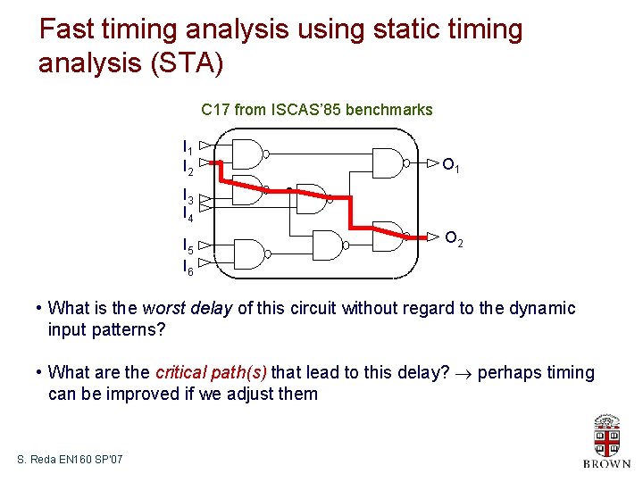
Fast timing analysis using static timing analysis (STA) C 17 from ISCAS’ 85 benchmarks I 1 I 2 O 1 I 3 I 4 I 5 I 6 O 2 • What is the worst delay of this circuit without regard to the dynamic input patterns? • What are the critical path(s) that lead to this delay? perhaps timing can be improved if we adjust them S. Reda EN 160 SP’ 07

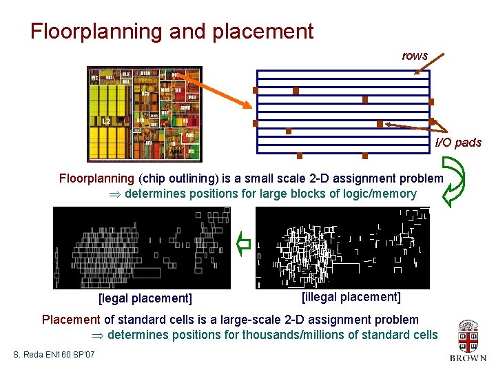
Floorplanning and placement rows I/O pads Floorplanning (chip outlining) is a small scale 2 -D assignment problem determines positions for large blocks of logic/memory [legal placement] [illegal placement] Placement of standard cells is a large-scale 2 -D assignment problem determines positions for thousands/millions of standard cells S. Reda EN 160 SP’ 07

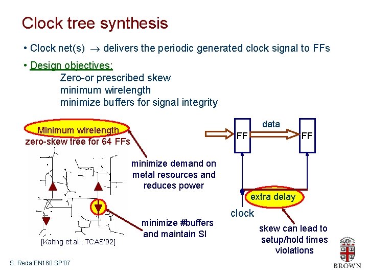
Clock tree synthesis • Clock net(s) delivers the periodic generated clock signal to FFs • Design objectives: Zero-or prescribed skew minimum wirelength minimize buffers for signal integrity data Minimum wirelength zero-skew tree for 64 FFs FF FF minimize demand on metal resources and reduces power extra delay [Kahng et al. , TCAS’ 92] S. Reda EN 160 SP’ 07 minimize #buffers and maintain SI clock skew can lead to setup/hold times violations

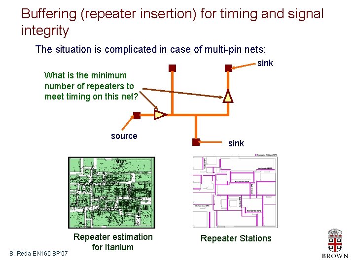
Buffering (repeater insertion) for timing and signal integrity The situation is complicated in case of multi-pin nets: sink What is the minimum number of repeaters to meet timing on this net? source S. Reda EN 160 SP’ 07 Repeater estimation for Itanium sink Repeater Stations

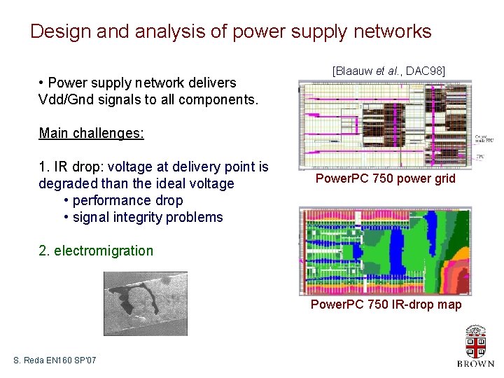
Design and analysis of power supply networks • Power supply network delivers Vdd/Gnd signals to all components. [Blaauw et al. , DAC 98] Main challenges: 1. IR drop: voltage at delivery point is degraded than the ideal voltage • performance drop • signal integrity problems Power. PC 750 power grid 2. electromigration Power. PC 750 IR-drop map S. Reda EN 160 SP’ 07

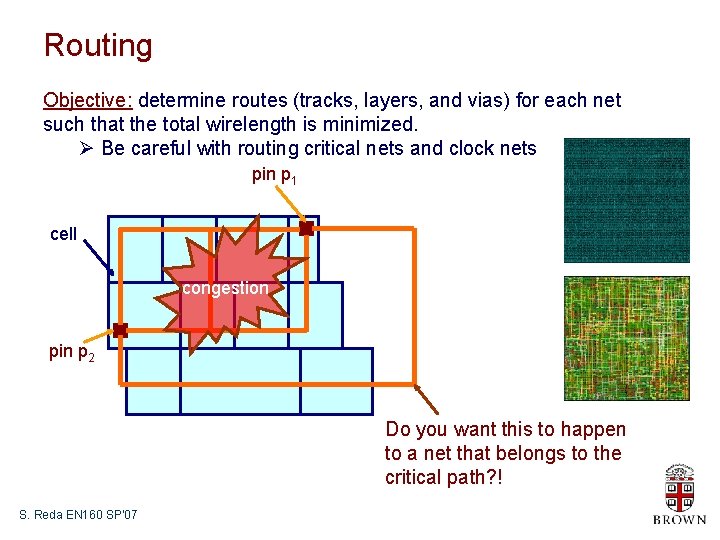
Routing Objective: determine routes (tracks, layers, and vias) for each net such that the total wirelength is minimized. Ø Be careful with routing critical nets and clock nets pin p 1 cell congestion pin p 2 Do you want this to happen to a net that belongs to the critical path? ! S. Reda EN 160 SP’ 07

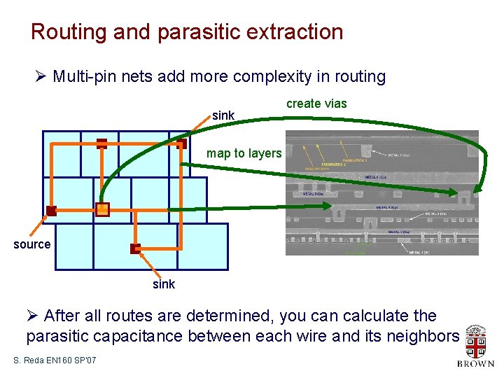
Routing and parasitic extraction Ø Multi-pin nets add more complexity in routing sink create vias map to layers source sink Ø After all routes are determined, you can calculate the parasitic capacitance between each wire and its neighbors S. Reda EN 160 SP’ 07

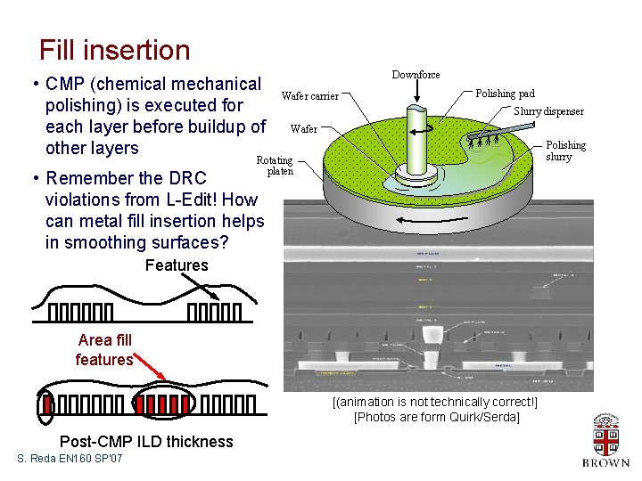
Fill insertion • CMP (chemical mechanical polishing) is executed for each layer before buildup of other layers Downforce Wafer carrier Polishing pad Slurry dispenser Wafer Polishing slurry Rotating platen • Remember the DRC violations from L-Edit! How can metal fill insertion helps in smoothing surfaces? Features Area fill features [(animation is not technically correct!] [Photos are form Quirk/Serda] Post-CMP ILD thickness S. Reda EN 160 SP’ 07

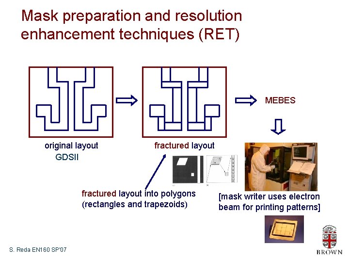
Mask preparation and resolution enhancement techniques (RET) MEBES original layout GDSII fractured layout into polygons (rectangles and trapezoids) S. Reda EN 160 SP’ 07 [mask writer uses electron beam for printing patterns]

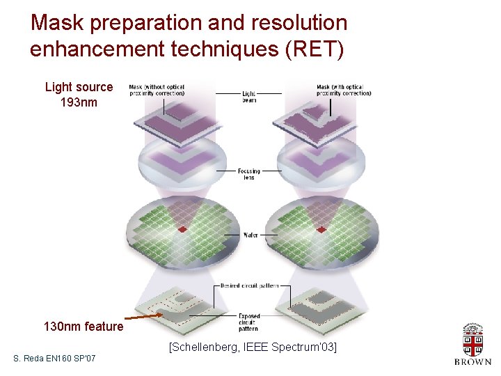
Mask preparation and resolution enhancement techniques (RET) Light source 193 nm 130 nm feature [Schellenberg, IEEE Spectrum’ 03] S. Reda EN 160 SP’ 07

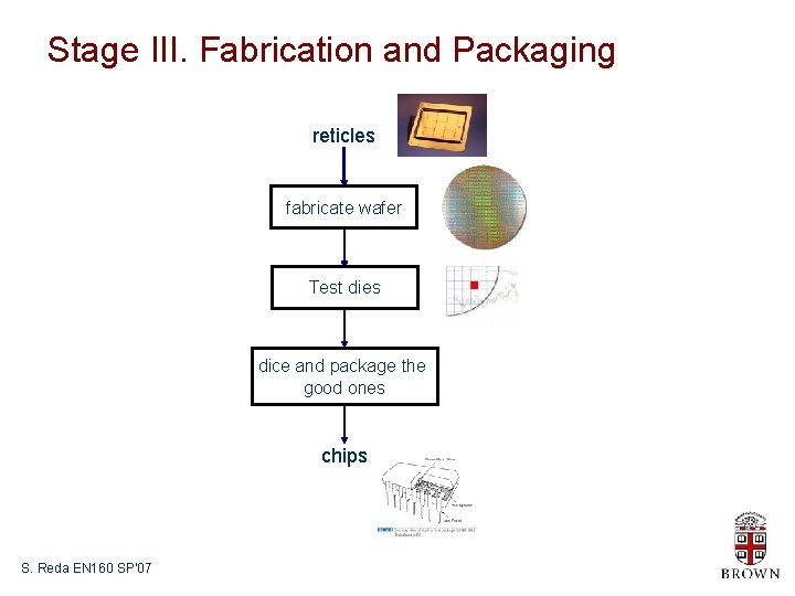
Stage III. Fabrication and Packaging reticles fabricate wafer Test dies dice and package the good ones chips S. Reda EN 160 SP’ 07

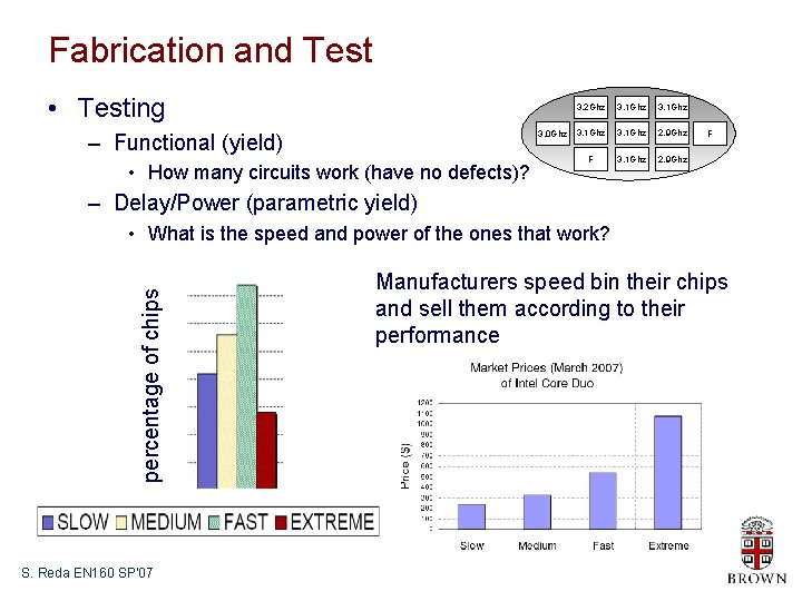
Fabrication and Test • Testing 3. 0 Ghz – Functional (yield) • How many circuits work (have no defects)? 3. 2 Ghz 3. 1 Ghz 2. 9 Ghz F 3. 1 Ghz 2. 9 Ghz F – Delay/Power (parametric yield) percentage of chips • What is the speed and power of the ones that work? S. Reda EN 160 SP’ 07 Manufacturers speed bin their chips and sell them according to their performance

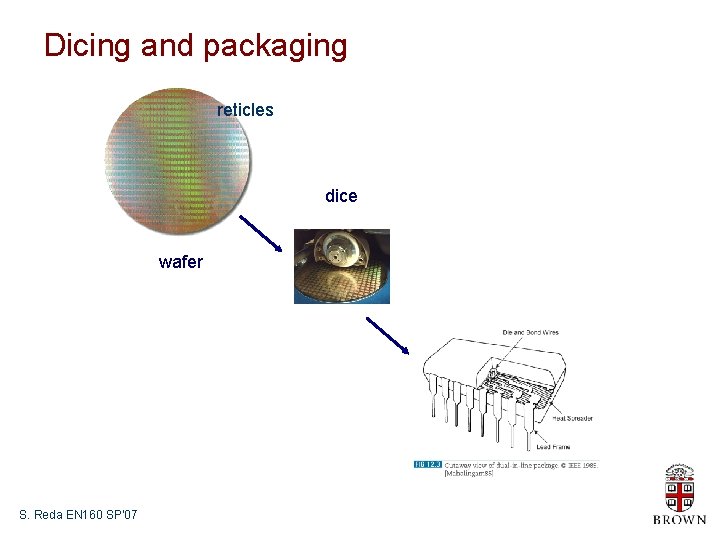
Dicing and packaging reticles dice wafer S. Reda EN 160 SP’ 07

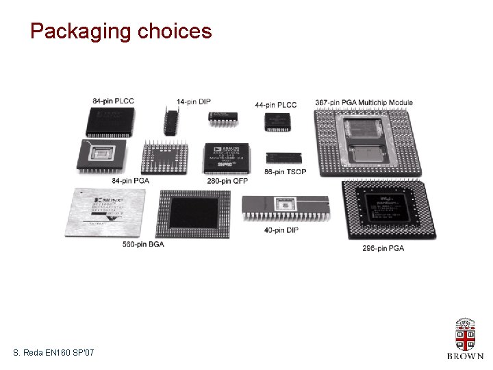
Packaging choices S. Reda EN 160 SP’ 07

Summary • Overview of IC design flow • We are done with main lectures • We meet in exactly one week on May 4 th to give your project presentations S. Reda EN 160 SP’ 07