Design and Implementation of VLSI Systems EN 0160
![NAND ROM V DD Pull-up devices BL [0] BL [1] BL [2] BL [3] NAND ROM V DD Pull-up devices BL [0] BL [1] BL [2] BL [3]](https://slidetodoc.com/presentation_image_h/b35b77c0846f5b72b4c550b461f0fc56/image-10.jpg)
- Slides: 17

Design and Implementation of VLSI Systems (EN 0160) Lecture 32: Array Subsystems (DRAM/ROM) Prof. Sherief Reda Division of Engineering, Brown University Spring 2007 [sources: Weste/Addison Wesley – Rabaey/Pearson] S. Reda EN 160 SP’ 07

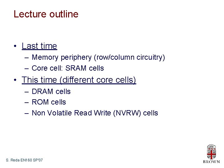
Lecture outline • Last time – Memory periphery (row/column circuitry) – Core cell: SRAM cells • This time (different core cells) – DRAM cells – ROM cells – Non Volatile Read Write (NVRW) cells S. Reda EN 160 SP’ 07

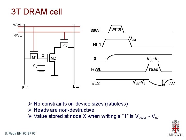
3 T DRAM cell WWL RWL write Vdd BL 1 M 3 M 1 X M 2 Cs BL 1 BL 2 X Vdd-Vt RWL read BL 2 Vdd-Vt Ø No constraints on device sizes (ratioless) Ø Reads are non-destructive Ø Value stored at node X when writing a “ 1” is VWWL - Vtn S. Reda EN 160 SP’ 07 V

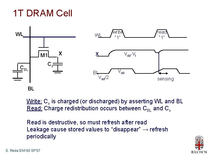
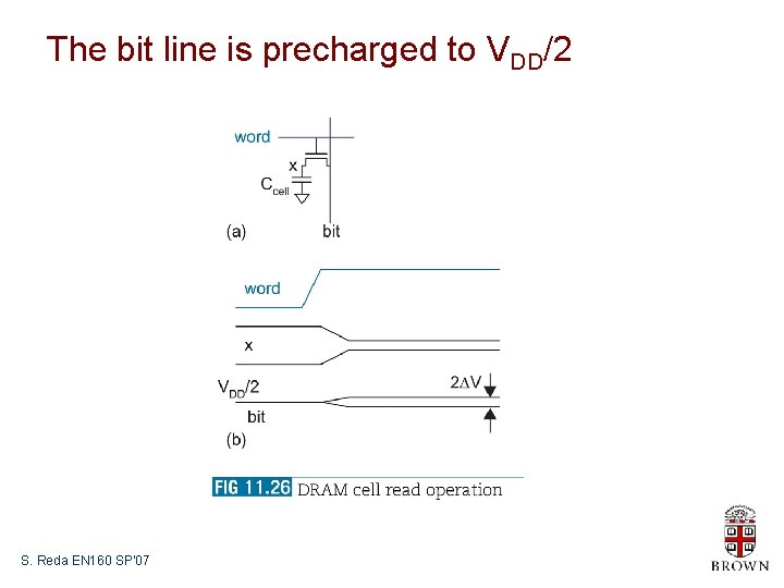
1 T DRAM Cell WL WL M 1 CBL X X write “ 1” read “ 1” Vdd-Vt Cs BL Vdd/2 Vdd sensing BL Write: Cs is charged (or discharged) by asserting WL and BL Read: Charge redistribution occurs between CBL and Cs Read is destructive, so must refresh after read Leakage cause stored values to “disappear” → refresh periodically S. Reda EN 160 SP’ 07

The bit line is precharged to VDD/2 S. Reda EN 160 SP’ 07

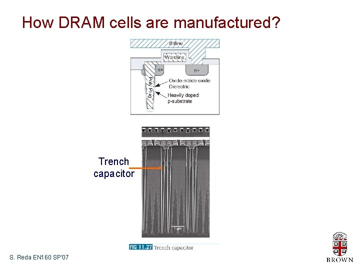
How DRAM cells are manufactured? Trench capacitor S. Reda EN 160 SP’ 07

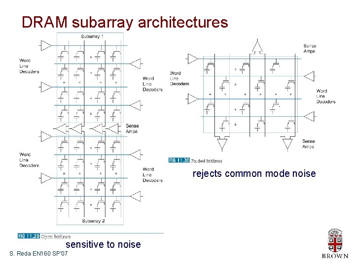
DRAM subarray architectures rejects common mode noise sensitive to noise S. Reda EN 160 SP’ 07

ROMs • Read-Only Memories are nonvolatile – Retain their contents when power is removed • Mask-programmed ROMs use one transistor per bit – Presence or absence determines 1 or 0 S. Reda EN 160 SP’ 07

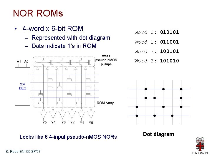
NOR ROMs • 4 -word x 6 -bit ROM – Represented with dot diagram – Dots indicate 1’s in ROM Word 0: 010101 Word 1: 011001 Word 2: 100101 Word 3: 101010 Looks like 6 4 -input pseudo-n. MOS NORs S. Reda EN 160 SP’ 07 Dot diagram
![NAND ROM V DD Pullup devices BL 0 BL 1 BL 2 BL 3 NAND ROM V DD Pull-up devices BL [0] BL [1] BL [2] BL [3]](https://slidetodoc.com/presentation_image_h/b35b77c0846f5b72b4c550b461f0fc56/image-10.jpg)
NAND ROM V DD Pull-up devices BL [0] BL [1] BL [2] BL [3] WL [0] WL [1] WL [2] WL [3] • All word lines high by default with exception of selected row • No transistor with the selected word -> bitline pulled down • Transistor with the selected word -> bitline remain high S. Reda EN 160 SP’ 07

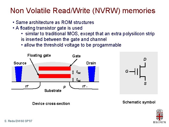
Non Volatile Read/Write (NVRW) memories • Same architecture as ROM structures • A floating transistor gate is used • similar to traditional MOS, except that an extra polysilicon strip is inserted between the gate and channel • allow the threshold voltage to be progammable Floating gate Gate Source Drain G tox n+ Substrate p Device cross-section S. Reda EN 160 SP’ 07 D n+_ S Schematic symbol

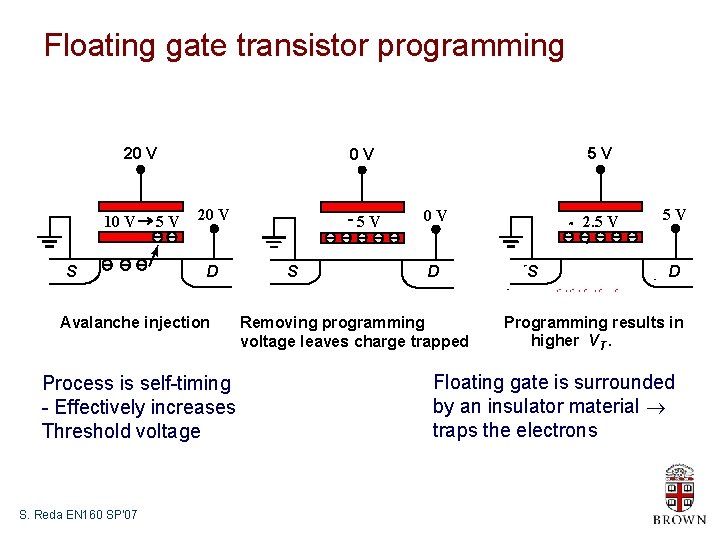
Floating gate transistor programming 20 V 10 V S 5 V 20 V D Avalanche injection Process is self-timing - Effectively increases Threshold voltage S. Reda EN 160 SP’ 07 5 V 0 V -5 V S 0 V D Removing programming voltage leaves charge trapped - 2. 5 V S 5 V D Programming results in higher V T. Floating gate is surrounded by an insulator material traps the electrons

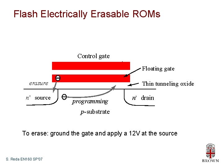
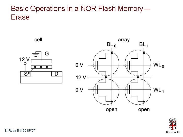
Flash Electrically Erasable ROMs Control gate Floating gate erasure n 1 source Thin tunneling oxide programming n 1 drain p-substrate To erase: ground the gate and apply a 12 V at the source S. Reda EN 160 SP’ 07

Basic Operations in a NOR Flash Memory― Erase S. Reda EN 160 SP’ 07

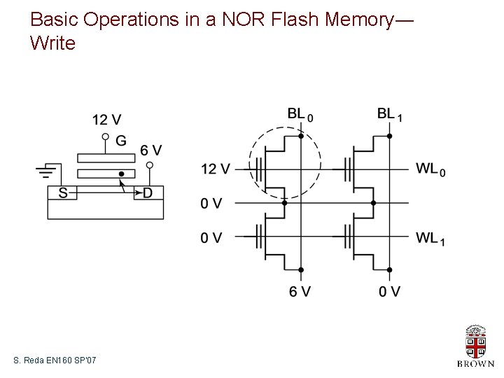
Basic Operations in a NOR Flash Memory― Write S. Reda EN 160 SP’ 07

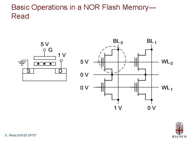
Basic Operations in a NOR Flash Memory― Read S. Reda EN 160 SP’ 07

Summary • So far, we covered – Periphery ( row decoders / column circuitry) – For the memory core: • • SRAM cells DRAM cells ROM NVWRM S. Reda EN 160 SP’ 07