CSCI 47175717 Computer Architecture Topic Cache Memory Reading

- Slides: 81

CSCI 4717/5717 Computer Architecture Topic: Cache Memory Reading: Stallings, Chapter 4 CSCI 4717 – Computer Architecture Cache Memory – Page 1 of 81

Characteristics of Memory “Location wrt Processor” • Inside CPU – temporary memory or registers • Inside processor – L 1 cache • Motherboard – main memory and L 2 cache • Main memory – DRAM and L 3 cache • External – peripherals such as disk, tape, and networked memory devices CSCI 4717 – Computer Architecture Cache Memory – Page 2 of 81

Characteristics of Memory “Capacity – Word Size” • The natural data size for a processor. • A 32 -bit processor has a 32 -bit word. • Typically based on processor's data bus width (i. e. , the width of an integer or an instruction) • Varying widths can be obtained by putting memory chips in parallel with same address lines CSCI 4717 – Computer Architecture Cache Memory – Page 3 of 81

Characteristics of Memory “Capacity – Addressable Units” • Varies based on the system's ability to allow addressing at byte level etc. • Typically smallest location which can be uniquely addressed • At mother board level, this is the word • It is a cluster on disks • Addressable units (N) equals 2 raised to the power of the number of bits in the address bus CSCI 4717 – Computer Architecture Cache Memory – Page 4 of 81

Characteristics of Memory “Unit of transfer” • The number of bits read out of or written into memory at a time. • Internal – Usually governed by data bus width, i. e. , a word • External – Usually a block which is much larger than a word CSCI 4717 – Computer Architecture Cache Memory – Page 5 of 81

Characteristics of Memory “Access method” • Based on the hardware implementation of the storage device • Four types – Sequential – Direct – Random – Associative CSCI 4717 – Computer Architecture Cache Memory – Page 6 of 81

Sequential Access Method • Start at the beginning and read through in order • Access time depends on location of data and previous location • Example: tape CSCI 4717 – Computer Architecture Cache Memory – Page 7 of 81

Direct Access Method • Individual blocks have unique address • Access is by jumping to vicinity then performing a sequential search • Access time depends on location of data within "block" and previous location • Example: hard disk CSCI 4717 – Computer Architecture Cache Memory – Page 8 of 81

Random Access Method • Individual addresses identify locations exactly • Access time is consistent across all locations and is independent previous access • Example: RAM CSCI 4717 – Computer Architecture Cache Memory – Page 9 of 81

Associative Access Method • Addressing information must be stored with data in a general data location • A specific data element is located by a comparing desired address with address portion of stored elements • Access time is independent of location or previous access • Example: cache CSCI 4717 – Computer Architecture Cache Memory – Page 10 of 81

Performance – Access Time • Time between "requesting" data and getting it • RAM – Time between putting address on bus and getting data. – It's predictable. • Other types, Sequential, Direct, Associative – Time it takes to position the read-write mechanism at the desired location. – Not predictable. CSCI 4717 – Computer Architecture Cache Memory – Page 11 of 81

Performance – Memory Cycle time • Primarily a RAM phenomenon • Adds "recovery" time to cycle allowing for transients to dissipate so that next access is reliable. • Cycle time is access + recovery CSCI 4717 – Computer Architecture Cache Memory – Page 12 of 81

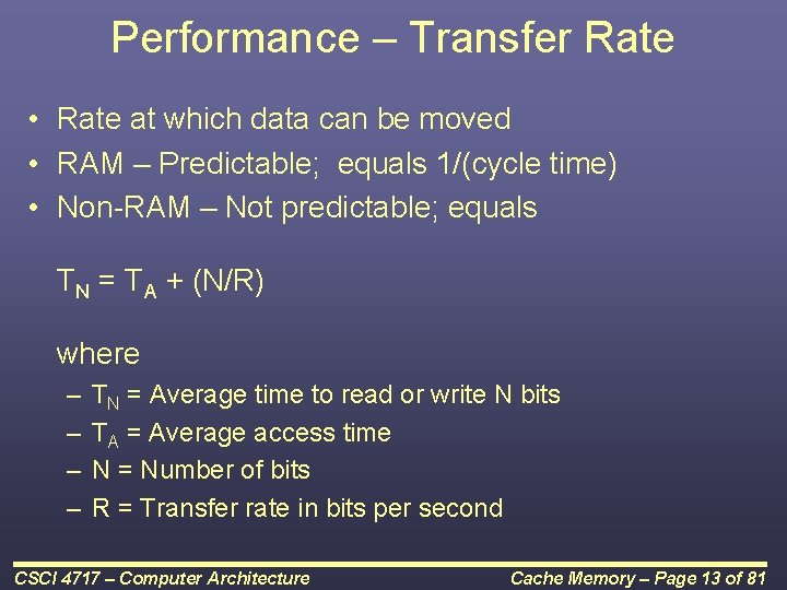
Performance – Transfer Rate • Rate at which data can be moved • RAM – Predictable; equals 1/(cycle time) • Non-RAM – Not predictable; equals TN = TA + (N/R) where – – TN = Average time to read or write N bits TA = Average access time N = Number of bits R = Transfer rate in bits per second CSCI 4717 – Computer Architecture Cache Memory – Page 13 of 81

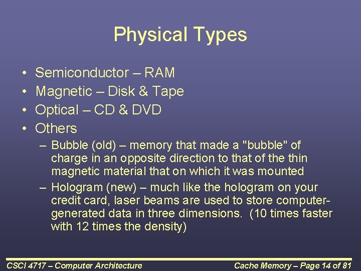
Physical Types • • Semiconductor – RAM Magnetic – Disk & Tape Optical – CD & DVD Others – Bubble (old) – memory that made a "bubble" of charge in an opposite direction to that of the thin magnetic material that on which it was mounted – Hologram (new) – much like the hologram on your credit card, laser beams are used to store computergenerated data in three dimensions. (10 times faster with 12 times the density) CSCI 4717 – Computer Architecture Cache Memory – Page 14 of 81

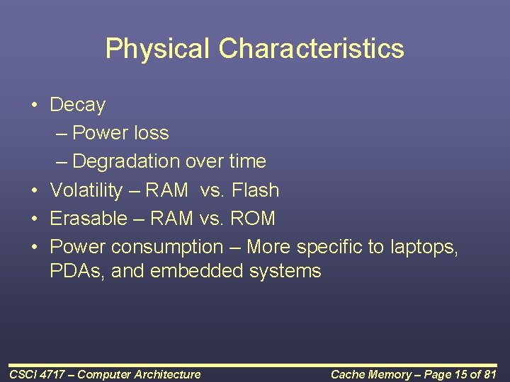
Physical Characteristics • Decay – Power loss – Degradation over time • Volatility – RAM vs. Flash • Erasable – RAM vs. ROM • Power consumption – More specific to laptops, PDAs, and embedded systems CSCI 4717 – Computer Architecture Cache Memory – Page 15 of 81

Organization • Physical arrangement of bits into words • Not always obvious • Non-sequential arrangements may be due to speed or reliability benefits, e. g. interleaved CSCI 4717 – Computer Architecture Cache Memory – Page 16 of 81

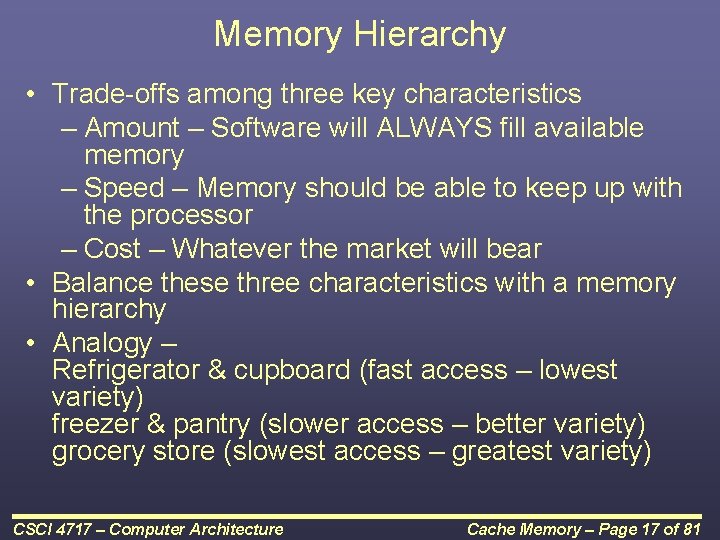
Memory Hierarchy • Trade-offs among three key characteristics – Amount – Software will ALWAYS fill available memory – Speed – Memory should be able to keep up with the processor – Cost – Whatever the market will bear • Balance these three characteristics with a memory hierarchy • Analogy – Refrigerator & cupboard (fast access – lowest variety) freezer & pantry (slower access – better variety) grocery store (slowest access – greatest variety) CSCI 4717 – Computer Architecture Cache Memory – Page 17 of 81

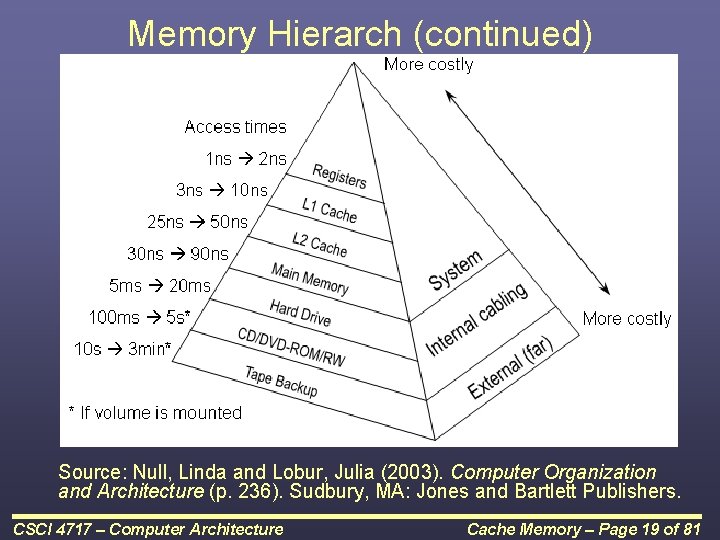
Memory Hierarch (continued) Implementation – Going down the hierarchy has the following results: – Decreasing cost per bit (cheaper) – Increasing capacity (larger) – Increasing access time (slower) – KEY – Decreasing frequency of access of the memory by the processor CSCI 4717 – Computer Architecture Cache Memory – Page 18 of 81

Memory Hierarch (continued) Source: Null, Linda and Lobur, Julia (2003). Computer Organization and Architecture (p. 236). Sudbury, MA: Jones and Bartlett Publishers. CSCI 4717 – Computer Architecture Cache Memory – Page 19 of 81

Mechanics of Technology • The basic mechanics of creating memory directly affect the first three characteristics of the hierarchy: – Decreasing cost per bit – Increasing capacity – Increasing access time • The fourth characteristic is met because of a principle known as locality of reference CSCI 4717 – Computer Architecture Cache Memory – Page 20 of 81

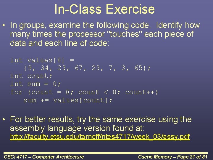
In-Class Exercise • In groups, examine the following code. Identify how many times the processor "touches" each piece of data and each line of code: int values[8] = {9, 34, 23, 67, 23, 7, 3, 65}; int count; int sum = 0; for (count = 0; count < 8; count++) sum += values[count]; • For better results, try the same exercise using the assembly language version found at: http: //faculty. etsu. edu/tarnoff/ntes 4717/week_03/assy. pdf CSCI 4717 – Computer Architecture Cache Memory – Page 21 of 81

Locality of Reference Due to the nature of programming, instructions and data tend to cluster together (loops, subroutines, and data structures) – Over a long period of time, clusters will change – Over a short period, clusters will tend to be the same CSCI 4717 – Computer Architecture Cache Memory – Page 22 of 81

Breaking Memory into Levels • Assume a hypothetical system has two levels of memory – Level 2 should contain all instructions and data – Level 1 doesn't have room for everything, so when a new cluster is required, the cluster it replaces must be sent back to the level 2 • These principles can be applied to much more than just two levels • If performance is based on amount of memory rather than speed, lower levels can be used to simulate larger sizes for higher levels, e. g. , virtual memory CSCI 4717 – Computer Architecture Cache Memory – Page 23 of 81

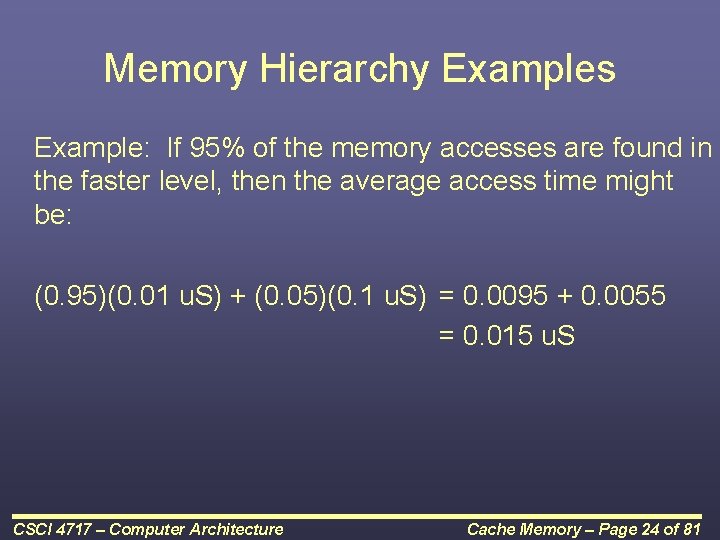
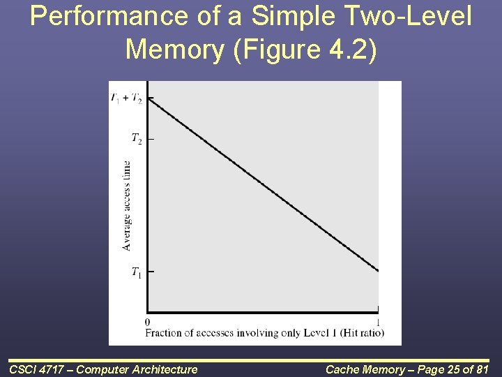
Memory Hierarchy Examples Example: If 95% of the memory accesses are found in the faster level, then the average access time might be: (0. 95)(0. 01 u. S) + (0. 05)(0. 1 u. S) = 0. 0095 + 0. 0055 = 0. 015 u. S CSCI 4717 – Computer Architecture Cache Memory – Page 24 of 81

Performance of a Simple Two-Level Memory (Figure 4. 2) CSCI 4717 – Computer Architecture Cache Memory – Page 25 of 81

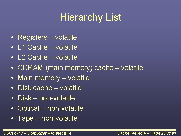
Hierarchy List • • • Registers – volatile L 1 Cache – volatile L 2 Cache – volatile CDRAM (main memory) cache – volatile Main memory – volatile Disk cache – volatile Disk – non-volatile Optical – non-volatile Tape – non-volatile CSCI 4717 – Computer Architecture Cache Memory – Page 26 of 81

Cache • What is it? A cache is a small amount of fast memory • What makes small fast? – Simpler decoding logic – More expensive SRAM technology – Close proximity to processor – Cache sits between normal main memory and CPU or it may be located on CPU chip or module CSCI 4717 – Computer Architecture Cache Memory – Page 27 of 81

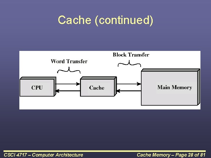
Cache (continued) CSCI 4717 – Computer Architecture Cache Memory – Page 28 of 81

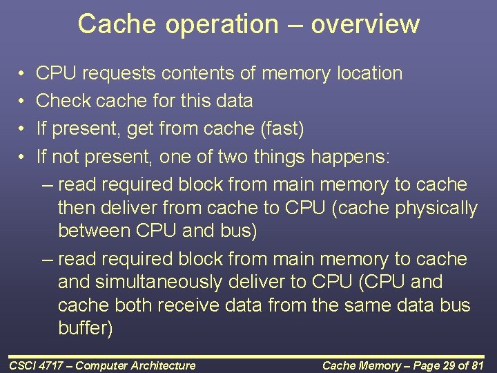
Cache operation – overview • • CPU requests contents of memory location Check cache for this data If present, get from cache (fast) If not present, one of two things happens: – read required block from main memory to cache then deliver from cache to CPU (cache physically between CPU and bus) – read required block from main memory to cache and simultaneously deliver to CPU (CPU and cache both receive data from the same data bus buffer) CSCI 4717 – Computer Architecture Cache Memory – Page 29 of 81

Going Deeper with Principle of Locality • Cache "misses" are unavoidable, i. e. , every piece of data and code thing must be loaded at least once • What does a processor do during a miss? It waits for the data to be loaded. • Power consumption varies linearly with clock speed and the square of the voltage. • Adjusting clock speed and voltage of processor has the potential to produce cubic (cubed root) power reductions (http: //www. visc. vt. edu/~mhsiao/papers/pacs 00 ch. pdf) • Identify places in in-class exercise where this might happen. CSCI 4717 – Computer Architecture Cache Memory – Page 30 of 81

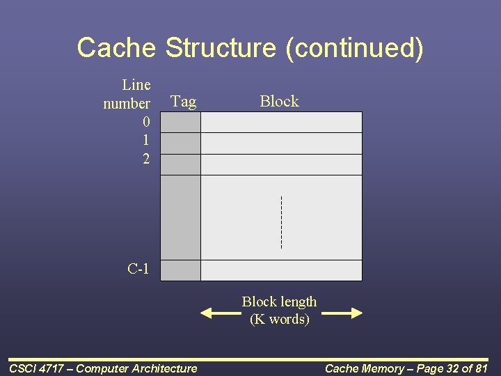
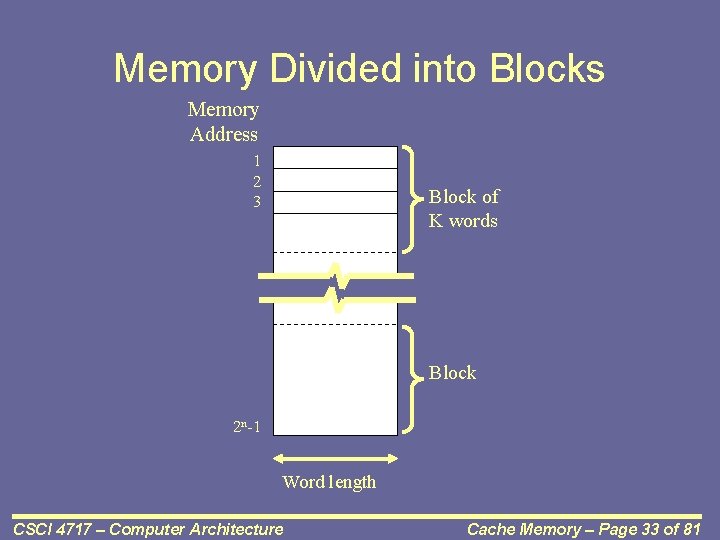
Cache Structure • Cache includes tags to identify the address of the block of main memory contained in a line of the cache • Each word in main memory has a unique n-bit address • There are M=2 n/K block of K words in main memory • Cache contains C lines of K words each plus a tag uniquely identifying the block of K words CSCI 4717 – Computer Architecture Cache Memory – Page 31 of 81

Cache Structure (continued) Line number 0 1 2 Tag Block C-1 Block length (K words) CSCI 4717 – Computer Architecture Cache Memory – Page 32 of 81

Memory Divided into Blocks Memory Address 1 2 3 Block of K words Block 2 n-1 Word length CSCI 4717 – Computer Architecture Cache Memory – Page 33 of 81

Cache Design • • • Size Mapping Function Replacement Algorithm Write Policy Block Size Number of Caches CSCI 4717 – Computer Architecture Cache Memory – Page 34 of 81

Cache size • Cost – More cache is expensive • Speed – More cache is faster (up to a point) – Larger decoding circuits slow up a cache – Algorithm is needed for mapping main memory addresses to lines in the cache. This takes more time than just a direct RAM CSCI 4717 – Computer Architecture Cache Memory – Page 35 of 81

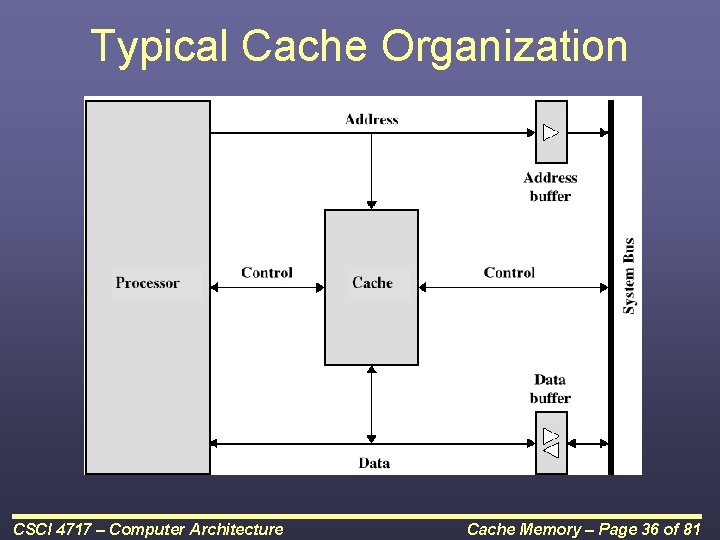
Typical Cache Organization CSCI 4717 – Computer Architecture Cache Memory – Page 36 of 81

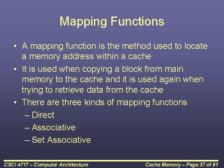
Mapping Functions • A mapping function is the method used to locate a memory address within a cache • It is used when copying a block from main memory to the cache and it is used again when trying to retrieve data from the cache • There are three kinds of mapping functions – Direct – Associative – Set Associative CSCI 4717 – Computer Architecture Cache Memory – Page 37 of 81

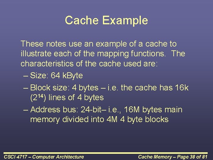
Cache Example These notes use an example of a cache to illustrate each of the mapping functions. The characteristics of the cache used are: – Size: 64 k. Byte – Block size: 4 bytes – i. e. the cache has 16 k (214) lines of 4 bytes – Address bus: 24 -bit– i. e. , 16 M bytes main memory divided into 4 M 4 byte blocks CSCI 4717 – Computer Architecture Cache Memory – Page 38 of 81

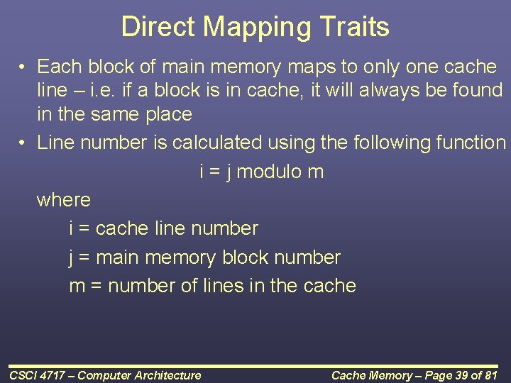
Direct Mapping Traits • Each block of main memory maps to only one cache line – i. e. if a block is in cache, it will always be found in the same place • Line number is calculated using the following function i = j modulo m where i = cache line number j = main memory block number m = number of lines in the cache CSCI 4717 – Computer Architecture Cache Memory – Page 39 of 81

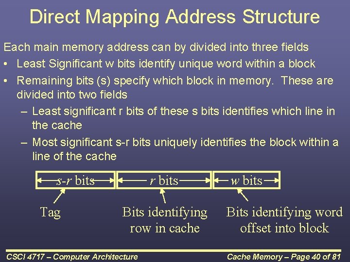
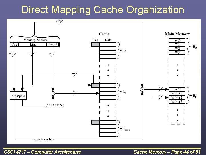
Direct Mapping Address Structure Each main memory address can by divided into three fields • Least Significant w bits identify unique word within a block • Remaining bits (s) specify which block in memory. These are divided into two fields – Least significant r bits of these s bits identifies which line in the cache – Most significant s-r bits uniquely identifies the block within a line of the cache s-r bits Tag r bits Bits identifying row in cache CSCI 4717 – Computer Architecture w bits Bits identifying word offset into block Cache Memory – Page 40 of 81

Direct Mapping Address Structure (continued) • Why are the r-bits used to identify which line in cache? • More likely to have unique r bits than s-r bits based on principle of locality of reference CSCI 4717 – Computer Architecture Cache Memory – Page 41 of 81

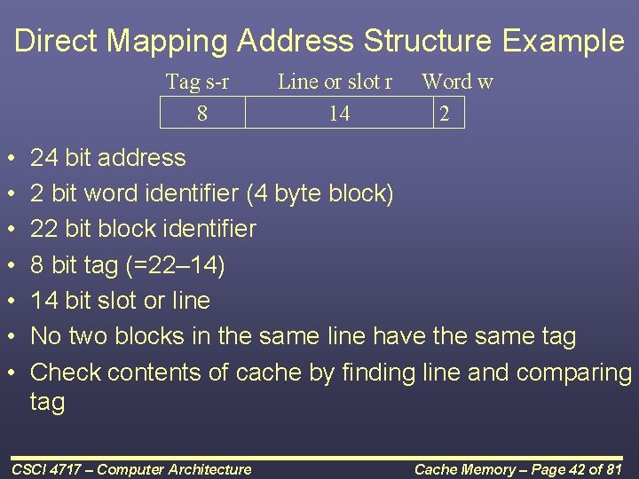
Direct Mapping Address Structure Example Tag s-r 8 • • Line or slot r 14 Word w 2 24 bit address 2 bit word identifier (4 byte block) 22 bit block identifier 8 bit tag (=22– 14) 14 bit slot or line No two blocks in the same line have the same tag Check contents of cache by finding line and comparing tag CSCI 4717 – Computer Architecture Cache Memory – Page 42 of 81

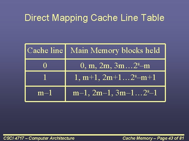
Direct Mapping Cache Line Table Cache line Main Memory blocks held 0 1 0, m, 2 m, 3 m… 2 s–m 1, m+1, 2 m+1… 2 s–m+1 m– 1, 2 m– 1, 3 m– 1… 2 s– 1 CSCI 4717 – Computer Architecture Cache Memory – Page 43 of 81

Direct Mapping Cache Organization CSCI 4717 – Computer Architecture Cache Memory – Page 44 of 81

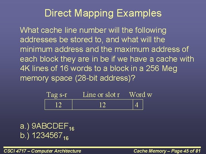
Direct Mapping Examples What cache line number will the following addresses be stored to, and what will the minimum address and the maximum address of each block they are in be if we have a cache with 4 K lines of 16 words to a block in a 256 Meg memory space (28 -bit address)? Tag s-r 12 Line or slot r 12 Word w 4 a. ) 9 ABCDEF 16 b. ) 123456716 CSCI 4717 – Computer Architecture Cache Memory – Page 45 of 81

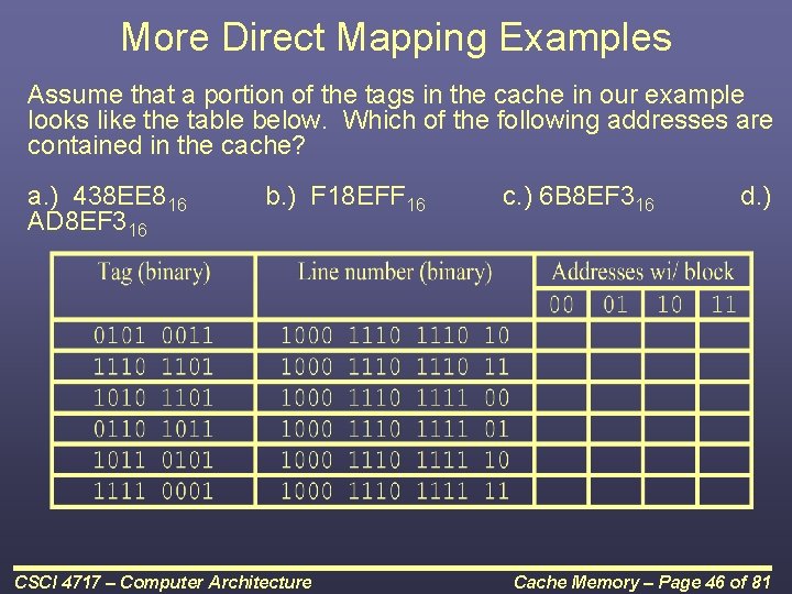
More Direct Mapping Examples Assume that a portion of the tags in the cache in our example looks like the table below. Which of the following addresses are contained in the cache? a. ) 438 EE 816 AD 8 EF 316 b. ) F 18 EFF 16 CSCI 4717 – Computer Architecture c. ) 6 B 8 EF 316 d. ) Cache Memory – Page 46 of 81

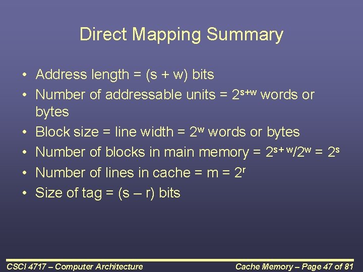
Direct Mapping Summary • Address length = (s + w) bits • Number of addressable units = 2 s+w words or bytes • Block size = line width = 2 w words or bytes • Number of blocks in main memory = 2 s+ w/2 w = 2 s • Number of lines in cache = m = 2 r • Size of tag = (s – r) bits CSCI 4717 – Computer Architecture Cache Memory – Page 47 of 81

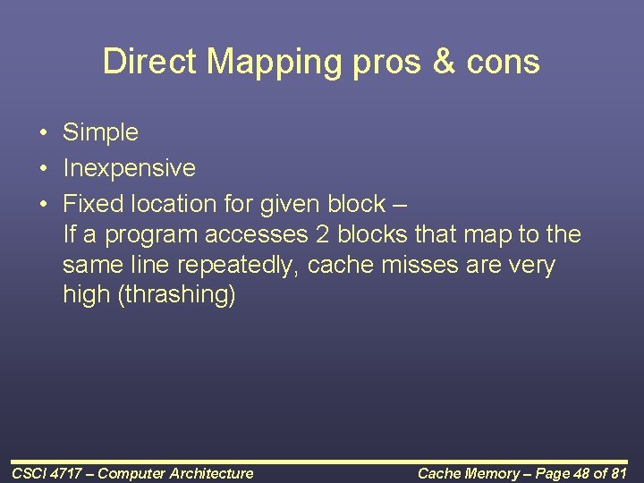
Direct Mapping pros & cons • Simple • Inexpensive • Fixed location for given block – If a program accesses 2 blocks that map to the same line repeatedly, cache misses are very high (thrashing) CSCI 4717 – Computer Architecture Cache Memory – Page 48 of 81

Associative Mapping Traits • A main memory block can load into any line of cache • Memory address is interpreted as: – Least significant w bits = word position within block – Most significant s bits = tag used to identify which block is stored in a particular line of cache • Every line's tag must be examined for a match • Cache searching gets expensive and slower CSCI 4717 – Computer Architecture Cache Memory – Page 49 of 81

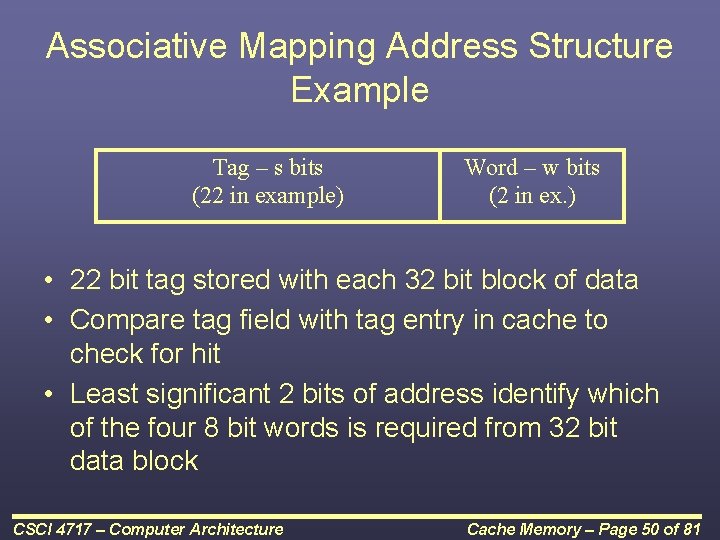
Associative Mapping Address Structure Example Tag – s bits (22 in example) Word – w bits (2 in ex. ) • 22 bit tag stored with each 32 bit block of data • Compare tag field with tag entry in cache to check for hit • Least significant 2 bits of address identify which of the four 8 bit words is required from 32 bit data block CSCI 4717 – Computer Architecture Cache Memory – Page 50 of 81

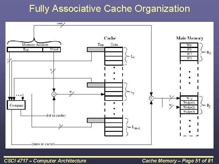
Fully Associative Cache Organization CSCI 4717 – Computer Architecture Cache Memory – Page 51 of 81

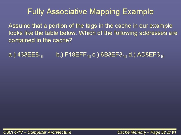
Fully Associative Mapping Example Assume that a portion of the tags in the cache in our example looks like the table below. Which of the following addresses are contained in the cache? a. ) 438 EE 816 b. ) F 18 EFF 16 c. ) 6 B 8 EF 316 d. ) AD 8 EF 316 CSCI 4717 – Computer Architecture Cache Memory – Page 52 of 81

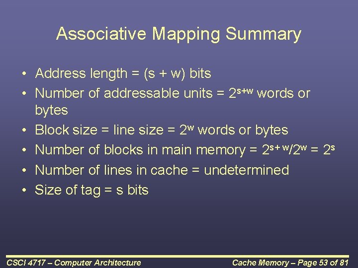
Associative Mapping Summary • Address length = (s + w) bits • Number of addressable units = 2 s+w words or bytes • Block size = line size = 2 w words or bytes • Number of blocks in main memory = 2 s+ w/2 w = 2 s • Number of lines in cache = undetermined • Size of tag = s bits CSCI 4717 – Computer Architecture Cache Memory – Page 53 of 81

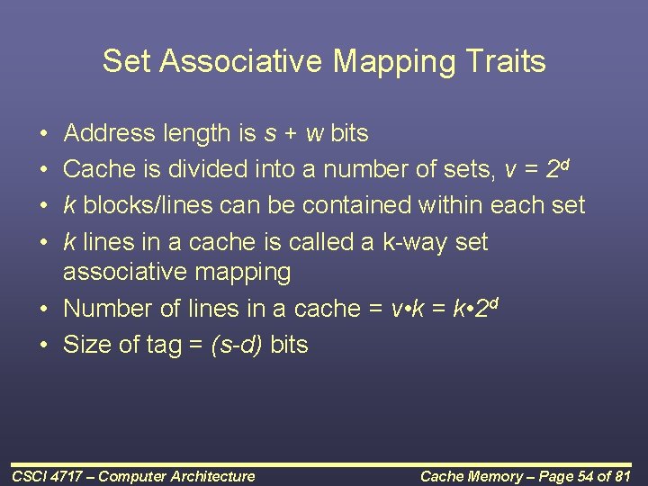
Set Associative Mapping Traits • • Address length is s + w bits Cache is divided into a number of sets, v = 2 d k blocks/lines can be contained within each set k lines in a cache is called a k-way set associative mapping • Number of lines in a cache = v • k = k • 2 d • Size of tag = (s-d) bits CSCI 4717 – Computer Architecture Cache Memory – Page 54 of 81

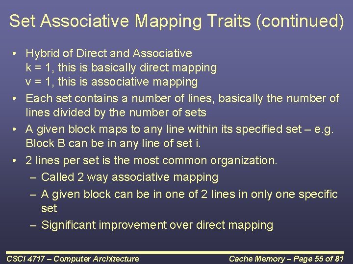
Set Associative Mapping Traits (continued) • Hybrid of Direct and Associative k = 1, this is basically direct mapping v = 1, this is associative mapping • Each set contains a number of lines, basically the number of lines divided by the number of sets • A given block maps to any line within its specified set – e. g. Block B can be in any line of set i. • 2 lines per set is the most common organization. – Called 2 way associative mapping – A given block can be in one of 2 lines in only one specific set – Significant improvement over direct mapping CSCI 4717 – Computer Architecture Cache Memory – Page 55 of 81

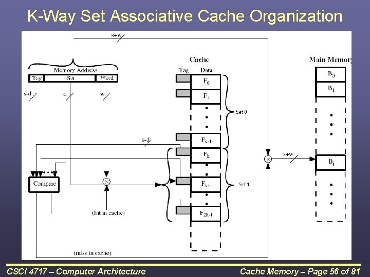
K-Way Set Associative Cache Organization CSCI 4717 – Computer Architecture Cache Memory – Page 56 of 81

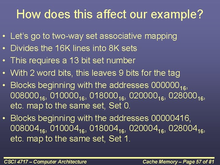
How does this affect our example? • • • Let’s go to two-way set associative mapping Divides the 16 K lines into 8 K sets This requires a 13 bit set number With 2 word bits, this leaves 9 bits for the tag Blocks beginning with the addresses 00000016, 00800016, 01000016, 01800016, 02000016, 02800016, etc. map to the same set, Set 0. • Blocks beginning with the addresses 00000416, 00800416, 01000416, 01800416, 02000416, 02800416, etc. map to the same set, Set 1. CSCI 4717 – Computer Architecture Cache Memory – Page 57 of 81

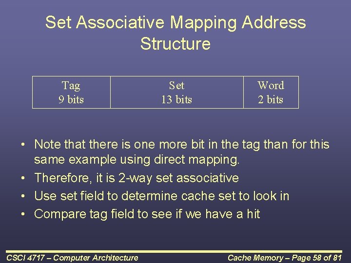
Set Associative Mapping Address Structure Tag 9 bits Set 13 bits Word 2 bits • Note that there is one more bit in the tag than for this same example using direct mapping. • Therefore, it is 2 -way set associative • Use set field to determine cache set to look in • Compare tag field to see if we have a hit CSCI 4717 – Computer Architecture Cache Memory – Page 58 of 81

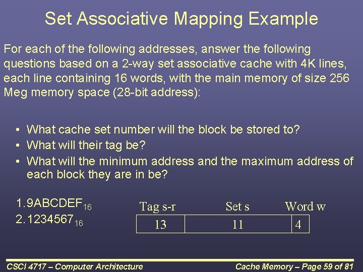
Set Associative Mapping Example For each of the following addresses, answer the following questions based on a 2 -way set associative cache with 4 K lines, each line containing 16 words, with the main memory of size 256 Meg memory space (28 -bit address): • What cache set number will the block be stored to? • What will their tag be? • What will the minimum address and the maximum address of each block they are in be? 1. 9 ABCDEF 16 2. 123456716 Tag s-r 13 CSCI 4717 – Computer Architecture Set s 11 Word w 4 Cache Memory – Page 59 of 81

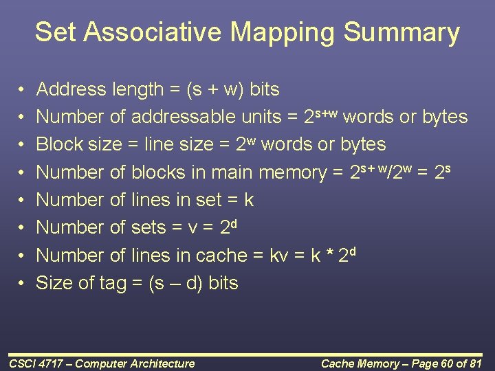
Set Associative Mapping Summary • • Address length = (s + w) bits Number of addressable units = 2 s+w words or bytes Block size = line size = 2 w words or bytes Number of blocks in main memory = 2 s+ w/2 w = 2 s Number of lines in set = k Number of sets = v = 2 d Number of lines in cache = kv = k * 2 d Size of tag = (s – d) bits CSCI 4717 – Computer Architecture Cache Memory – Page 60 of 81

Replacement Algorithms • There must be a method for selecting which line in the cache is going to be replaced when there’s no room for a new line • Hardware implemented algorithm (speed) • Direct mapping – There is no need for a replacement algorithm with direct mapping – Each block only maps to one line – Replace that line CSCI 4717 – Computer Architecture Cache Memory – Page 61 of 81

Associative & Set Associative Replacement Algorithms • Least Recently used (LRU) – Replace the block that hasn't been touched in the longest period of time – Two way set associative simply uses a USE bit. When one block is referenced, its USE bit is set while its partner in the set is cleared • First in first out (FIFO) – replace block that has been in cache longest CSCI 4717 – Computer Architecture Cache Memory – Page 62 of 81

Associative & Set Associative Replacement Algorithms (continued) • Least frequently used (LFU) – replace block which has had fewest hits • Random – only slightly lower performance than use-based algorithms LRU, FIFO, and LFU CSCI 4717 – Computer Architecture Cache Memory – Page 63 of 81

Writing to Cache • Must not overwrite a cache block unless main memory is up to date • Two main problems: – If cache is written to, main memory is invalid or if main memory is written to, cache is invalid – Can occur if I/O can address main memory directly – Multiple CPUs may have individual caches; once one cache is written to, all caches are invalid CSCI 4717 – Computer Architecture Cache Memory – Page 64 of 81

Write through • All writes go to main memory as well as cache • Multiple CPUs can monitor main memory traffic to keep local (to CPU) cache up to date • Lots of traffic • Slows down writes CSCI 4717 – Computer Architecture Cache Memory – Page 65 of 81

Write back • Updates initially made in cache only • Update bit for cache slot is set when update occurs • If block is to be replaced, write to main memory only if update bit is set • Other caches get out of sync • I/O must access main memory through cache • Research shows that 15% of memory references are writes CSCI 4717 – Computer Architecture Cache Memory – Page 66 of 81

Multiple Processors/Multiple Caches • Even if a write through policy is used, other processors may have invalid data in their caches • In other words, if a processor updates its cache and updates main memory, a second processor may have been using the same data in its own cache which is now invalid. CSCI 4717 – Computer Architecture Cache Memory – Page 67 of 81

Solutions to Prevent Problems with Multiprocessor/cache systems • Bus watching with write through – each cache watches the bus to see if data they contain is being written to the main memory by another processor. All processors must be using the write through policy • Hardware transparency – a "big brother" watches all caches, and upon seeing an update to any processor's cache, it updates main memory AND all of the caches • Noncacheable memory – Any shared memory (identified with a chip select) may not be cached. CSCI 4717 – Computer Architecture Cache Memory – Page 68 of 81

Line Size • There is a relationship between line size (i. e. , the number of words in a line in the cache) and hit ratios • As the line size (block size) goes up, the hit ratio could go up due to more words available to the principle of locality of reference • As block size increases, however, the number of blocks goes down, and the hit ratio will begin to go back down after a while • Lastly, as the block size increases, the chances of a hit to a word farther from the initially referenced word goes down CSCI 4717 – Computer Architecture Cache Memory – Page 69 of 81

Multi-Level Caches • Increases in transistor densities have allowed for caches to be placed inside processor chip • Internal caches have very short wires (within the chip itself) and are therefore quite fast, even faster then any zero wait-state memory accesses outside of the chip • This means that a super fast internal cache (level 1) can be inside of the chip while an external cache (level 2) can provide access faster then to main memory CSCI 4717 – Computer Architecture Cache Memory – Page 70 of 81

Unified versus Split Caches • Split into two caches – one for instructions, one for data • Disadvantages – Questionable as unified cache balances data and instructions merely with hit rate. – Hardware is simpler with unified cache • Advantage – What a split cache is really doing is providing one cache for the instruction decoder and one for the execution unit. – This supports pipelined architectures. CSCI 4717 – Computer Architecture Cache Memory – Page 71 of 81

Intel x 86 caches • 80386 – no on chip cache • 80486 – 8 k using 16 byte lines and four-way set associative organization (main memory had 32 address lines – 4 Gig) • Pentium (all versions) – Two on chip L 1 caches – Data & instructions CSCI 4717 – Computer Architecture Cache Memory – Page 72 of 81

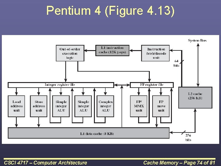
Pentium 4 L 1 and L 2 Caches • L 1 cache – 8 k bytes – 64 byte lines – Four way set associative • L 2 cache – – Feeding both L 1 caches 256 k 128 byte lines 8 way set associative CSCI 4717 – Computer Architecture Cache Memory – Page 73 of 81

Pentium 4 (Figure 4. 13) CSCI 4717 – Computer Architecture Cache Memory – Page 74 of 81

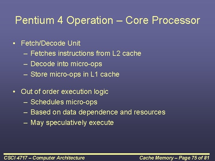
Pentium 4 Operation – Core Processor • Fetch/Decode Unit – Fetches instructions from L 2 cache – Decode into micro-ops – Store micro-ops in L 1 cache • Out of order execution logic – Schedules micro-ops – Based on data dependence and resources – May speculatively execute CSCI 4717 – Computer Architecture Cache Memory – Page 75 of 81

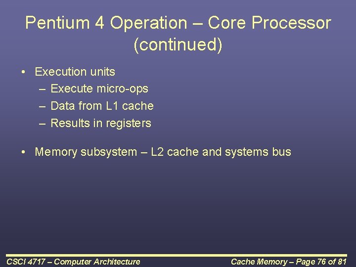
Pentium 4 Operation – Core Processor (continued) • Execution units – Execute micro-ops – Data from L 1 cache – Results in registers • Memory subsystem – L 2 cache and systems bus CSCI 4717 – Computer Architecture Cache Memory – Page 76 of 81

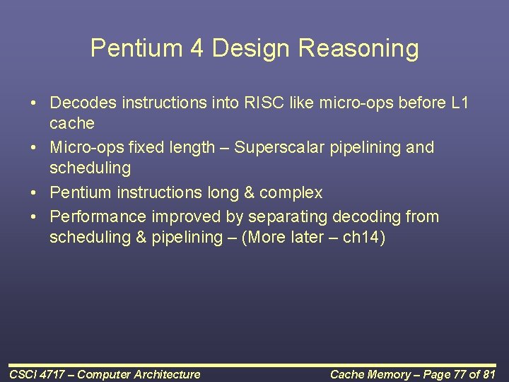
Pentium 4 Design Reasoning • Decodes instructions into RISC like micro-ops before L 1 cache • Micro-ops fixed length – Superscalar pipelining and scheduling • Pentium instructions long & complex • Performance improved by separating decoding from scheduling & pipelining – (More later – ch 14) CSCI 4717 – Computer Architecture Cache Memory – Page 77 of 81

Pentium 4 Design Reasoning (continued) • Data cache is write back – Can be configured to write through • L 1 cache controlled by 2 bits in register – CD = cache disable – NW = not write through – 2 instructions to invalidate (flush) cache and write back then invalidate CSCI 4717 – Computer Architecture Cache Memory – Page 78 of 81

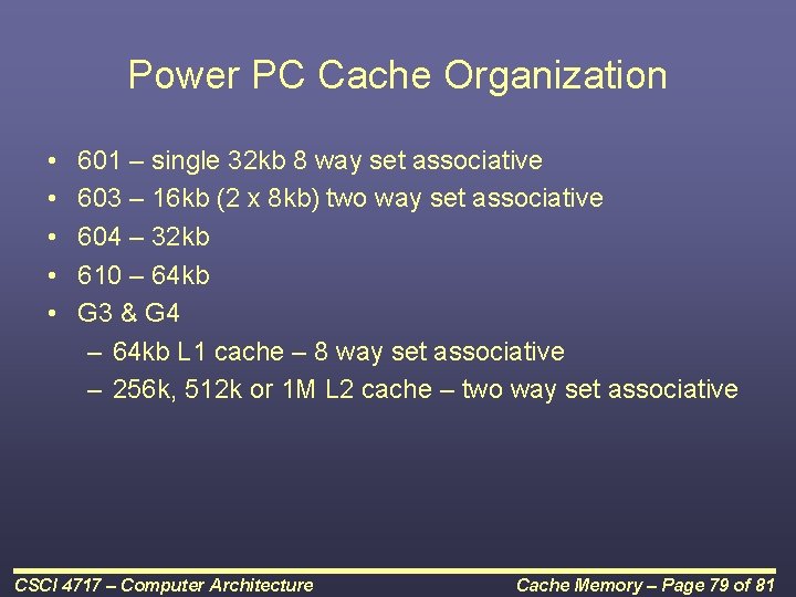
Power PC Cache Organization • • • 601 – single 32 kb 8 way set associative 603 – 16 kb (2 x 8 kb) two way set associative 604 – 32 kb 610 – 64 kb G 3 & G 4 – 64 kb L 1 cache – 8 way set associative – 256 k, 512 k or 1 M L 2 cache – two way set associative CSCI 4717 – Computer Architecture Cache Memory – Page 79 of 81

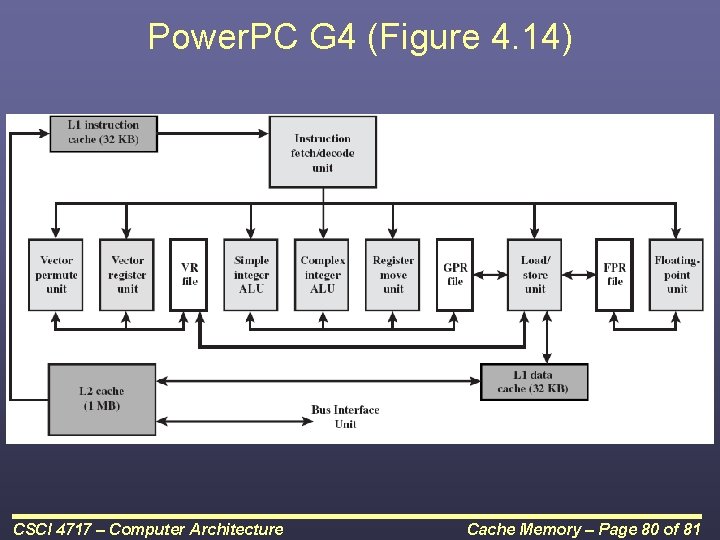
Power. PC G 4 (Figure 4. 14) CSCI 4717 – Computer Architecture Cache Memory – Page 80 of 81

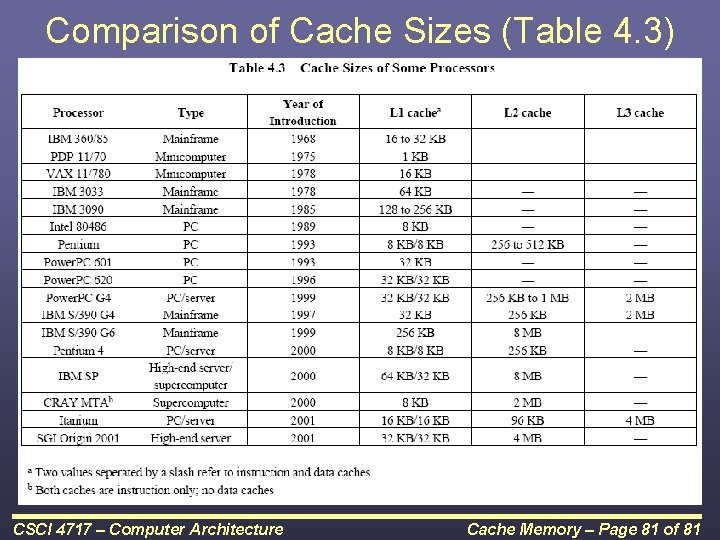
Comparison of Cache Sizes (Table 4. 3) CSCI 4717 – Computer Architecture Cache Memory – Page 81 of 81