Course 2 deciphering a schematic CERN Summer school
- Slides: 29

Course 2 : deciphering a schematic CERN Summer school 2003 C. de LA TAILLE LAL Orsay 9 -11 july 2003 C. de La Taille@lal. in 2 p 3. fr Electronics CERN Summer School 2003 1

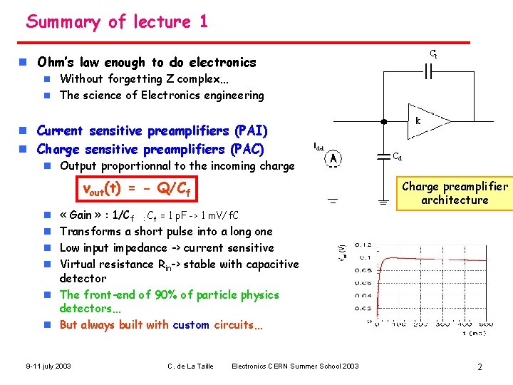
Summary of lecture 1 n Ohm’s law enough to do electronics Without forgetting Z complex… n The science of Electronics engineering n n Current sensitive preamplifiers (PAI) n Charge sensitive preamplifiers (PAC) n Output proportionnal to the incoming charge vout(t) = - Q/Cf « Gain » : 1/Cf : Cf = 1 p. F -> 1 m. V/f. C Transforms a short pulse into a long one Low input impedance -> current sensitive Virtual resistance Rin-> stable with capacitive detector n The front-end of 90% of particle physics detectors… n But always built with custom circuits… Charge preamplifier architecture n n 9 -11 july 2003 C. de La Taille Electronics CERN Summer School 2003 2

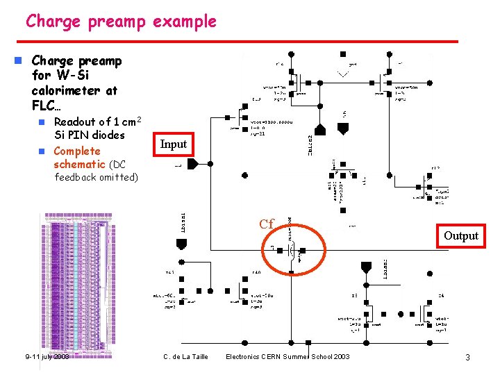
Charge preamp example n Charge preamp for W-Si calorimeter at FLC… Readout of 1 cm 2 Si PIN diodes n Complete schematic (DC n Input feedback omitted) Cf 9 -11 july 2003 C. de La Taille Electronics CERN Summer School 2003 Output 3

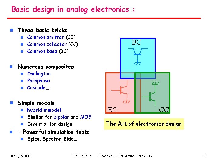
Basic design in analog electronics : n Three basic bricks Common emitter (CE) n Common collector (CC) n Common base (BC) n n BC Numerous composites Darlington n Paraphase n Cascode… n n Simple models hybrid π model n Similar for bipolar and MOS n Essential for design n n + Powerful simulation tools n EC CC The Art of electronics design Spice, Spectre, Eldo… 9 -11 july 2003 C. de La Taille Electronics CERN Summer School 2003 4

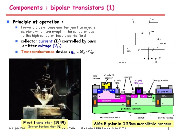
Components : bipolar transistors (1) n Principle of operation : n Forward bias of base emitter junction injects carriers which are swept in the collector due to the high collector-base electric field collector current (IC) controlled by base -emitter voltage (VBE) n Transconductance device : gm = ∂IC /∂VBE n First transistor (1949) 9 -11 july 2003 (Brattain-Bardeen Nobel 56) C. de La Taille Si. Ge Bipolar in 0. 35µm monolithic process Electronics CERN Summer School 2003 5

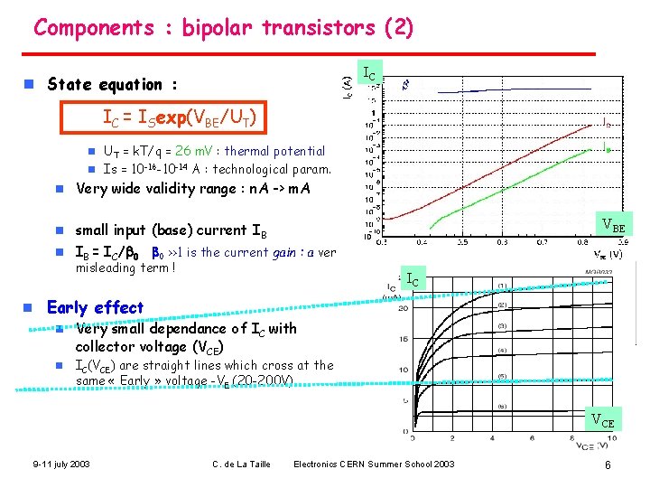
Components : bipolar transistors (2) IC n State equation : IC = ISexp(VBE/UT) n UT = k. T/q = 26 m. V : thermal potential n Is = 10 -16 -10 -14 A : technological param. n Very wide validity range : n. A -> m. A VBE small input (base) current IB n IB = IC/b 0 >>1 is the current gain : a very n misleading term ! n IC Early effect n n Very small dependance of IC with collector voltage (VCE) IC(VCE) are straight lines which cross at the same « Early » voltage -VE (20 -200 V) VCE 9 -11 july 2003 C. de La Taille Electronics CERN Summer School 2003 6

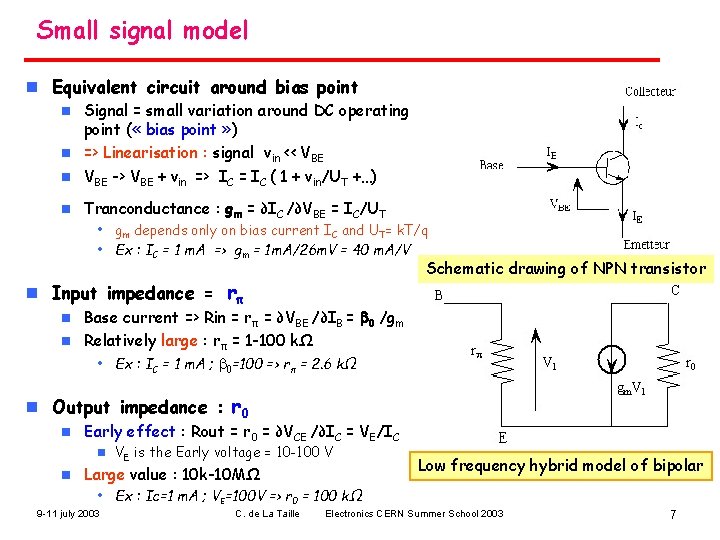
Small signal model n Equivalent circuit around bias point Signal = small variation around DC operating point ( « bias point » ) n => Linearisation : signal vin << VBE n VBE -> VBE + vin => IC = IC ( 1 + vin/UT +…) n n Tranconductance : gm = ∂IC /∂VBE = IC/UT • gm depends only on bias current IC and UT= k. T/q • Ex : IC = 1 m. A => gm = 1 m. A/26 m. V = 40 m. A/V Schematic drawing of NPN transistor n Input impedance = rπ Base current => Rin = rπ = ∂VBE /∂IB = b 0 /gm n Relatively large : rπ = 1 -100 kΩ • Ex : IC = 1 m. A ; b 0=100 => rπ = 2. 6 kΩ n n Output impedance : r 0 n Early effect : Rout = r 0 = ∂VCE /∂IC = VE/IC n VE is the Early voltage = 10 -100 V n Large value : 10 k-10 MΩ Low frequency hybrid model of bipolar • Ex : Ic=1 m. A ; VE=100 V => r 0 = 100 kΩ 9 -11 july 2003 C. de La Taille Electronics CERN Summer School 2003 7

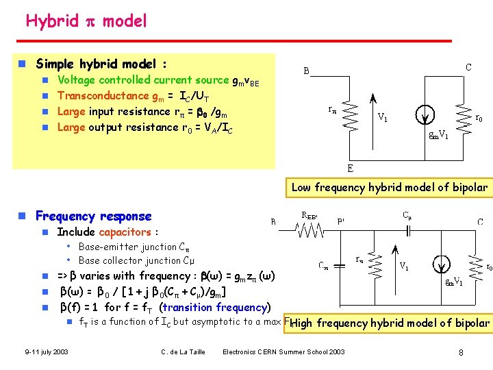
Hybrid p model n Simple hybrid model : Voltage controlled current source gmv. BE n Transconductance gm = IC/UT n Large input resistance rπ = b 0 /gm n Large output resistance r 0 = VA/IC n Low frequency hybrid model of bipolar n Frequency response n Include capacitors : • Base-emitter junction Cπ • Base collector junction Cμ => β varies with frequency : b(ω) = gmzπ (ω) n β(ω) = β 0 / [ 1 + j β 0(Cπ + Cμ)/gm] n β(f) = 1 for f = f. T (transition frequency) n n f. T is a function of IC but asymptotic to a max FHigh T 9 -11 july 2003 C. de La Taille frequency hybrid model of bipolar Electronics CERN Summer School 2003 8

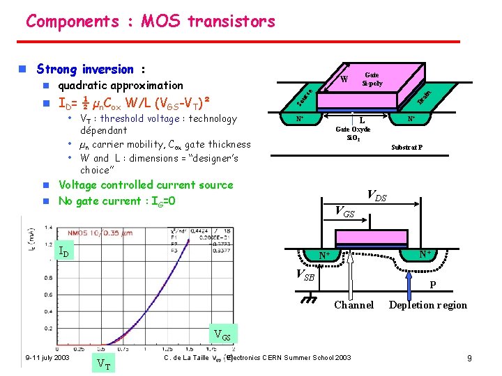
Components : MOS transistors n Strong inversion : n ai Dr ID= ½ µn. Cox W/L (VGS-VT)² ce n ur quadratic approximation Gate Si-poly So n W • VT : threshold voltage : technology dépendant • µn carrier mobility, Cox gate thickness • W and L : dimensions = “designer’s choice” N+ N+ L Gate Oxyde Si. O 2 Substrat P Voltage controlled current source n No gate current : IG=0 n VGS ID VDS N+ N+ VSB P Channel Depletion region VGS 9 -11 july 2003 VT C. de La Taille Electronics CERN Summer School 2003 9

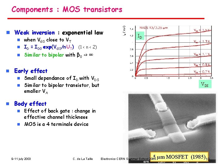
Components : MOS transistors n Weak inversion : exponential law when VGS close to VT n ID = ID 0 exp(VGS/n. UT) (1 < n < 2) n n n ID Similar to bipolar with β 0 -> ∞ Early effect Small dependance of ID with VDS n Similar to bipolar transistor, but smaller VA n n VDS Body effect Effect of back gate : change in effective channel thickness n MOS is a 4 terminals device n 9 -11 july 2003 C. de La Taille 5 µm MOSFET (1985)10 Electronics CERN Summer School 2003

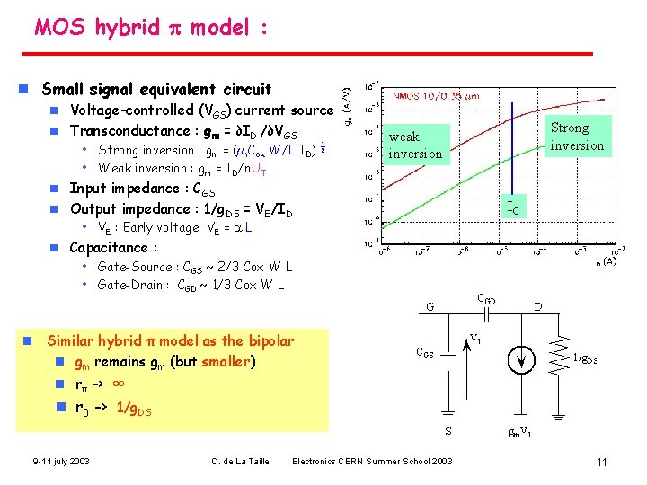
MOS hybrid p model : n Small signal equivalent circuit Voltage-controlled (VGS) current source (ID) n Transconductance : gm = ∂ID /∂VGS n • Strong inversion : gm = (µn. Cox W/L ID) ½ • Weak inversion : gm = ID/n. UT Strong inversion weak inversion Input impedance : CGS n Output impedance : 1/g. DS = VE/ID n IC • VE : Early voltage VE = a L n Capacitance : • Gate-Source : CGS ~ 2/3 Cox W L • Gate-Drain : CGD ~ 1/3 Cox W L n Similar hybrid π model as the bipolar n gm remains gm (but smaller) n rπ -> ∞ n r 0 -> 1/g. DS 9 -11 july 2003 C. de La Taille Electronics CERN Summer School 2003 11

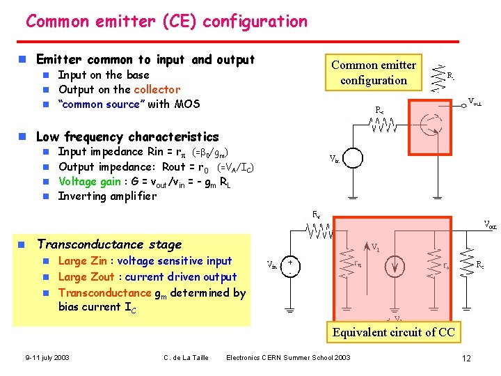
Common emitter (CE) configuration n Emitter common to input and output Input on the base n Output on the collector n “common source” with MOS n Common emitter configuration n Low frequency characteristics Input impedance Rin = rp (=b 0/gm) n Output impedance: Rout = r 0 (=VA/IC) n Voltage gain : G = vout/vin = - gm RL n Inverting amplifier n n Transconductance stage Large Zin : voltage sensitive input n Large Zout : current driven output n Transconductance gm determined by bias current IC n Equivalent circuit of CC 9 -11 july 2003 C. de La Taille Electronics CERN Summer School 2003 12

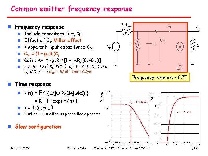
Common emitter frequency response n Frequency response n n n Include capacitors : Cπ, Cμ Effect of Cμ: Miller effect = apparent input capacitance CMi = (1 + gm. RL)Cμ Gain : Av = -gm. RL/[1 + jw. RS(Cπ+CMi)] Ex : RS=1 kΩ RL=20 kΩ gm=1 m. A/V Cπ=2. 5 p. F Cμ=0. 5 p. F => CMi = 10 p. F tau=12. 5 ns Frequency response of CE n Time response n H(t) = F -1 { 1/jω R/(1+jωRC) } = R [ 1 - exp(-t/ τ) ] n τ = RS(Cπ+CMi) n Similar calculation as photodiode preamp n Slow configuration 9 -11 july 2003 C. de La Taille Electronics CERN Summer School 2003 13

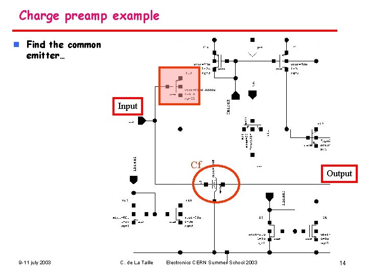
Charge preamp example n Find the common emitter… Input Cf 9 -11 july 2003 C. de La Taille Electronics CERN Summer School 2003 Output 14

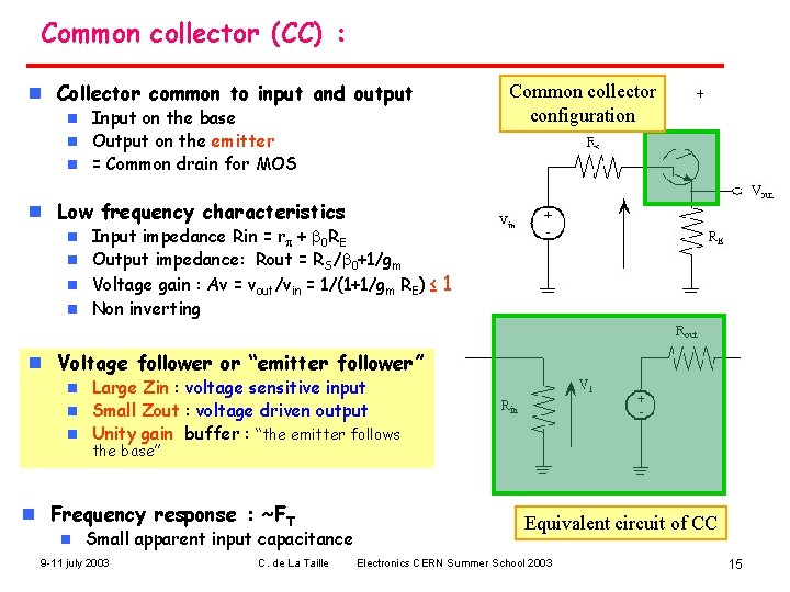
Common collector (CC) : n Collector common to input and output Input on the base n Output on the emitter n = Common drain for MOS n Common collector configuration n Low frequency characteristics Input impedance Rin = rp + b 0 RE n Output impedance: Rout = RS/b 0+1/gm n Voltage gain : Av = vout/vin = 1/(1+1/gm RE) ≤ 1 n Non inverting n n Voltage follower or “emitter follower” Large Zin : voltage sensitive input n Small Zout : voltage driven output n Unity gain buffer : “the emitter follows n the base” n Frequency response : ~FT n Small apparent input capacitance 9 -11 july 2003 C. de La Taille Equivalent circuit of CC Electronics CERN Summer School 2003 15

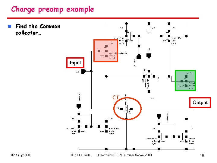
Charge preamp example n Find the Common collector… Input Cf 9 -11 july 2003 C. de La Taille Electronics CERN Summer School 2003 Output 16

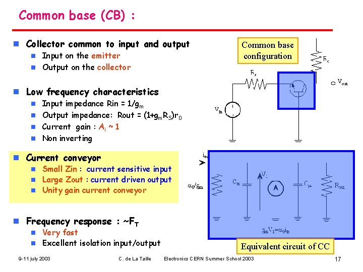
Common base (CB) : n Collector common to input and output Input on the emitter n Output on the collector n Common base configuration n Low frequency characteristics Input impedance Rin = 1/gm n Output impedance: Rout = (1+gm. RS)r 0 n Current gain : Ai ~ 1 n Non inverting n n Current conveyor Small Zin : current sensitive input n Large Zout : current driven output n Unity gain current conveyor n n Frequency response : ~FT Very fast n Excellent isolation input/output n 9 -11 july 2003 C. de La Taille Equivalent circuit of CC Electronics CERN Summer School 2003 17

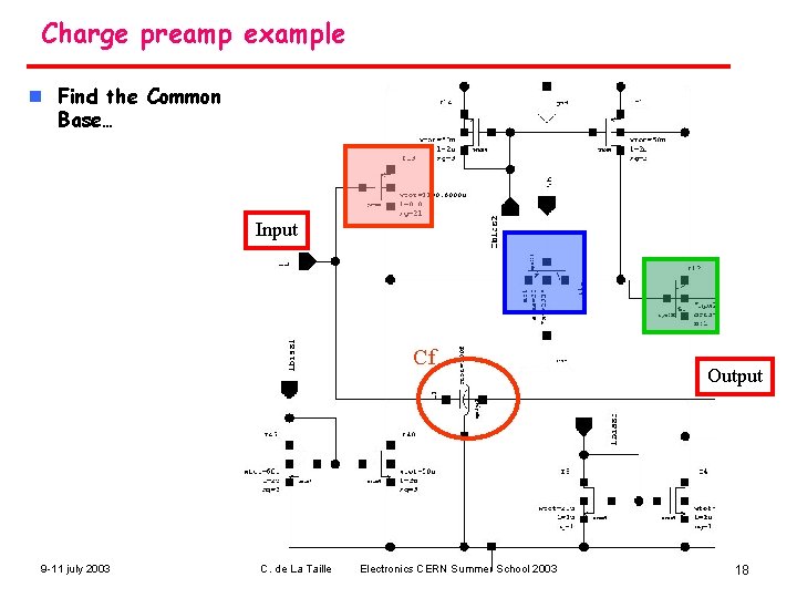
Charge preamp example n Find the Common Base… Input Cf 9 -11 july 2003 C. de La Taille Electronics CERN Summer School 2003 Output 18

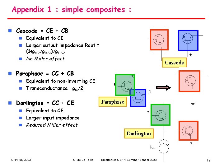
Appendix 1 : simple composites : n Cascode = CE + CB Equivalent to CE n Larger output impedance Rout = (1+gm 2/g. DS 1)/g. DS 2 n No Miller effect n Cascode n Paraphase = CC + CB Equivalent to non-inverting CE n Transconductance : gm/2 n n Darlington = CC + CE Paraphase Equivalent to CE n Larger input impedance n Reduced Miller effect n Darlington 9 -11 july 2003 C. de La Taille Electronics CERN Summer School 2003 19

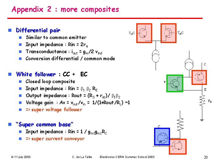
Appendix 2 : more composites n Differential pair Similar to common emitter n Input impedance : Rin = 2 rp n Transconductance : iout = gm/2 vind n Conversion differential / common mode n n White follower : CC + EC n n n Closed loop composite Input impedance : Rin = b 1 b 2 RE Output impedance : Rout = (RS + rp 1)/ b 1 b 2 Voltage gain : Av = vout/vin = 1/(1+Rout/RL) ~1 => super voltage follower n “Super common base” Input impedance : Rin = 1 / gm 1 gm 2 RC n => super current conveyor n 9 -11 july 2003 C. de La Taille Electronics CERN Summer School 2003 20

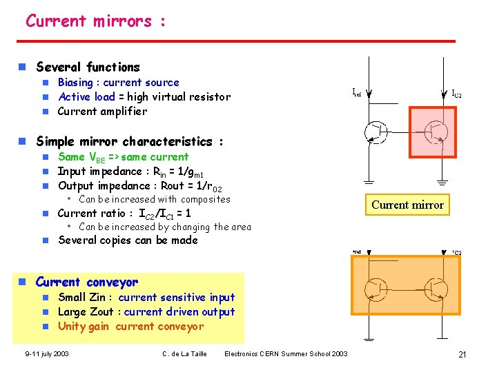
Current mirrors : n Several functions Biasing : current source n Active load = high virtual resistor n Current amplifier n n Simple mirror characteristics : Same VBE => same current n Input impedance : Rin = 1/gm 1 n Output impedance : Rout = 1/r 02 n • Can be increased with composites n Current ratio : IC 2/IC 1 = 1 Current mirror • Can be increased by changing the area n Several copies can be made n Current conveyor Small Zin : current sensitive input n Large Zout : current driven output n Unity gain current conveyor n 9 -11 july 2003 C. de La Taille Electronics CERN Summer School 2003 21

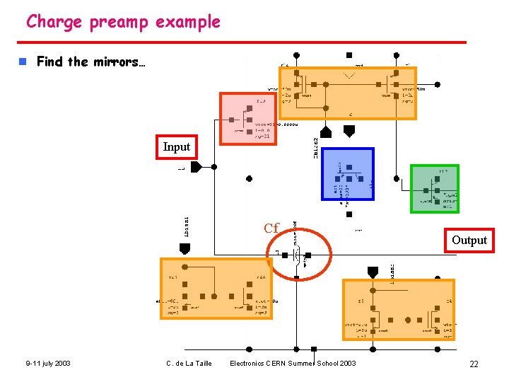
Charge preamp example n Find the mirrors… Input Cf 9 -11 july 2003 C. de La Taille Electronics CERN Summer School 2003 Output 22

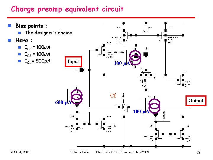
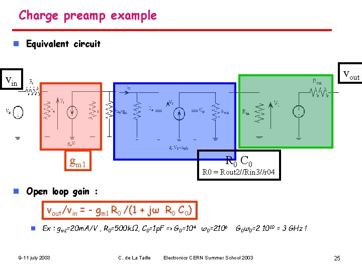
Charge preamp equivalent circuit n Bias points : n The designer’s choice n Here : IC 3 = 100µA n IC 2 = 100µA n IC 1 = 500µA n Input 100 µA Cf Output 600 µA 100 µA 9 -11 july 2003 C. de La Taille Electronics CERN Summer School 2003 23

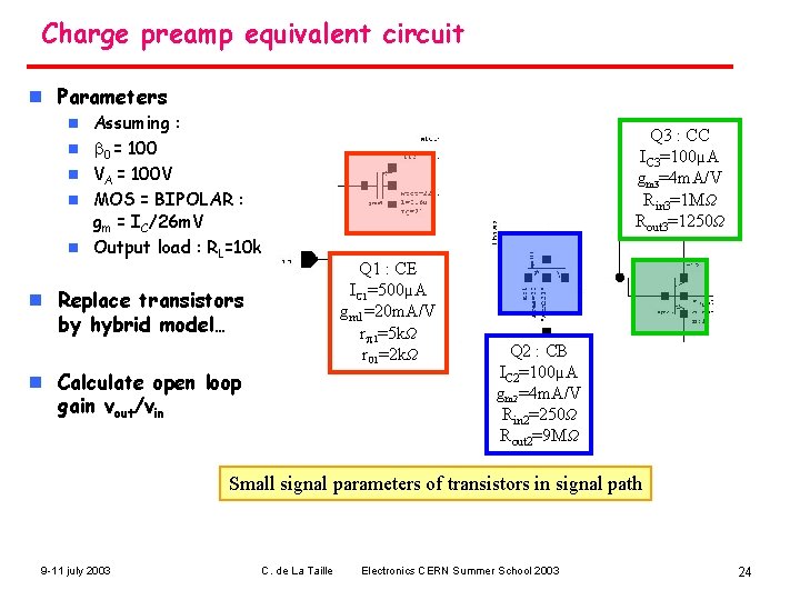
Charge preamp equivalent circuit n Parameters n n n Assuming : b 0 = 100 VA = 100 V MOS = BIPOLAR : gm = IC/26 m. V Output load : RL=10 k n Replace transistors by hybrid model… n Calculate open loop gain vout/vin Q 3 : CC IC 3=100µA gm 3=4 m. A/V Rin 3=1 MΩ Rout 3=1250Ω Q 1 : CE IC 1=500µA gm 1=20 m. A/V rp 1=5 kΩ r 01=2 kΩ Q 2 : CB IC 2=100µA gm 2=4 m. A/V Rin 2=250Ω Rout 2=9 MΩ Small signal parameters of transistors in signal path 9 -11 july 2003 C. de La Taille Electronics CERN Summer School 2003 24

Charge preamp example n Equivalent circuit vout vin R 0 C 0 gm 1 R 0 = Rout 2//Rin 3//r 04 n Open loop gain : vout/vin = - gm 1 R 0 /(1 + jω R 0 C 0) n Ex : gm 1=20 m. A/V , R 0=500 kΩ, C 0=1 p. F => G 0=104 ω0=2106 9 -11 july 2003 C. de La Taille G 0ω0=2 1010 = 3 GHz ! Electronics CERN Summer School 2003 25

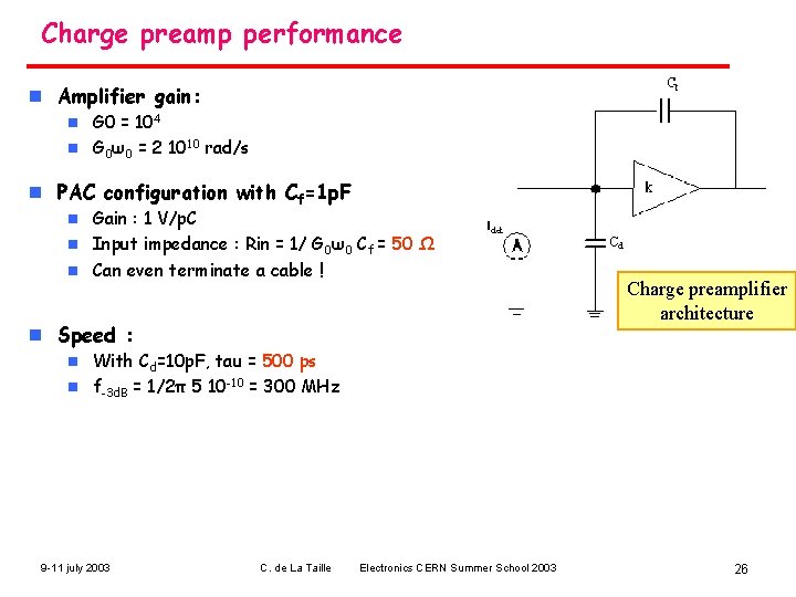
Charge preamp performance n Amplifier gain: G 0 = 104 n G 0ω0 = 2 1010 rad/s n n PAC configuration with Cf=1 p. F Gain : 1 V/p. C n Input impedance : Rin = 1/ G 0ω0 Cf = 50 Ω n Can even terminate a cable ! n n Speed : Charge preamplifier architecture With Cd=10 p. F, tau = 500 ps n f-3 d. B = 1/2π 5 10 -10 = 300 MHz n 9 -11 july 2003 C. de La Taille Electronics CERN Summer School 2003 26

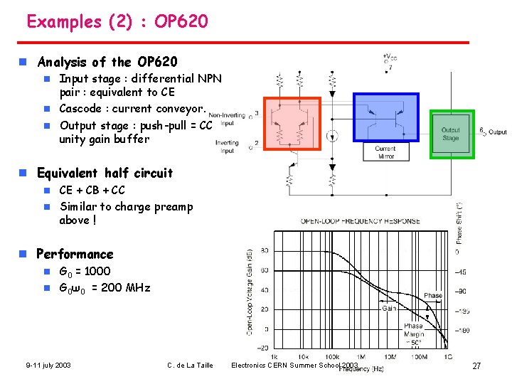
Examples (2) : OP 620 n Analysis of the OP 620 Input stage : differential NPN pair : equivalent to CE n Cascode : current conveyor. n Output stage : push-pull = CC unity gain buffer n n Equivalent half circuit CE + CB + CC n Similar to charge preamp above ! n n Performance G 0 = 1000 n G 0ω0 = 200 MHz n 9 -11 july 2003 C. de La Taille Electronics CERN Summer School 2003 27

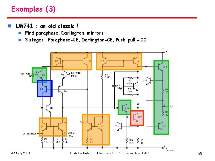
Examples (3) n LM 741 : an old classic ! Find paraphase, Darlington, mirrors n 3 stages : Paraphase=CE, Darlington=CE, Push-pull = CC n G 0 = 200 000, GBW = 1 MHz n 9 -11 july 2003 C. de La Taille Electronics CERN Summer School 2003 28

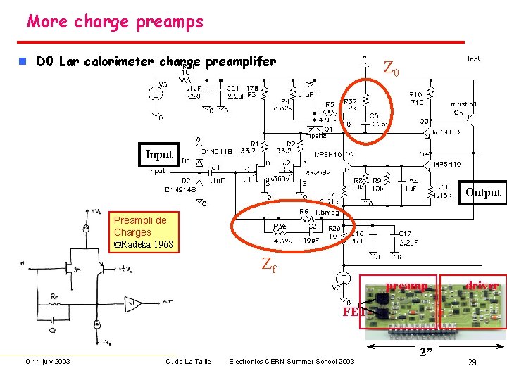
More charge preamps n D 0 Lar calorimeter charge preamplifer Z 0 Input Output Préampli de Charges ©Radeka 1968 Zf preamp driver FET 9 -11 july 2003 C. de La Taille Electronics CERN Summer School 2003 2” 29