Chapter 27 Diodes and Diode Applications Topics Covered
- Slides: 43

Chapter 27 Diodes and Diode Applications Topics Covered in Chapter 27 • 27 -1: Semiconductor Materials • 27 -2: The PN Junction Diode • 27 -3: Volt-Ampere Characteristic Curve • 27 -4: Diode Approximations • 27 -5: Diode Ratings • 27 -6: Rectifier Diodes • 27 -7: Special Diodes © 2007 The Mc. Graw-Hill Companies, Inc. All rights reserved.

27 -1: Semiconductor Materials § Semiconductors conduct less than metal conductors but more than insulators. § Some common semiconductor materials are silicon (Si), germanium (Ge), and carbon (C). § Silicon is the most widely used semiconductor material in the electronics industry. § Almost all diodes, transistors, and ICs manufactured today are made from silicon.

27 -1: Semiconductor Materials § Intrinsic semiconductors are semiconductors in their purest form. § Extrinsic semiconductors are semiconductors with other atoms mixed in. § These other atoms are called impurity atoms. § The process of adding impurity atoms is called doping.

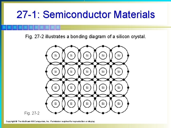
27 -1: Semiconductor Materials Fig. 27 -2 illustrates a bonding diagram of a silicon crystal. Fig. 27 -2 Copyright © The Mc. Graw-Hill Companies, Inc. Permission required for reproduction or display.

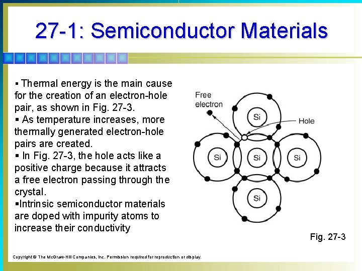
27 -1: Semiconductor Materials § Thermal energy is the main cause for the creation of an electron-hole pair, as shown in Fig. 27 -3. § As temperature increases, more thermally generated electron-hole pairs are created. § In Fig. 27 -3, the hole acts like a positive charge because it attracts a free electron passing through the crystal. §Intrinsic semiconductor materials are doped with impurity atoms to increase their conductivity Copyright © The Mc. Graw-Hill Companies, Inc. Permission required for reproduction or display. Fig. 27 -3

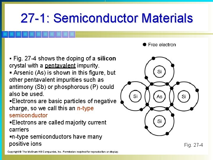
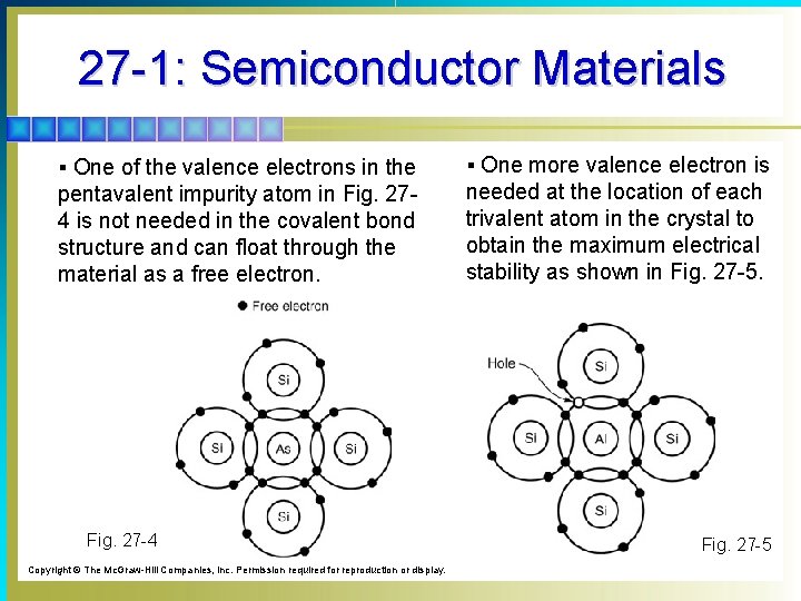
27 -1: Semiconductor Materials § Fig. 27 -4 shows the doping of a silicon crystal with a pentavalent impurity. § Arsenic (As) is shown in this figure, but other pentavalent impurities such as antimony (Sb) or phosphorous (P) could also be used. §Electrons are basic particles of negative charge, so we call this an n-type semiconductor §Electrons are called majority current carriers §n-type semiconductors have many positive ions Copyright © The Mc. Graw-Hill Companies, Inc. Permission required for reproduction or display. Fig. 27 -4

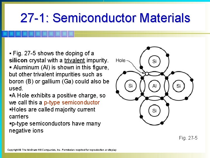
27 -1: Semiconductor Materials § Fig. 27 -5 shows the doping of a silicon crystal with a trivalent impurity. § Aluminum (Al) is shown in this figure, but other trivalent impurities such as boron (B) or gallium (Ga) could also be used. §A Hole exhibits a positive charge, so we call this a p-type semiconductor §Holes are called majority current carriers §p-type semiconductors have many negative ions Fig. 27 -5 Copyright © The Mc. Graw-Hill Companies, Inc. Permission required for reproduction or display.

27 -1: Semiconductor Materials § One of the valence electrons in the pentavalent impurity atom in Fig. 274 is not needed in the covalent bond structure and can float through the material as a free electron. Fig. 27 -4 Copyright © The Mc. Graw-Hill Companies, Inc. Permission required for reproduction or display. § One more valence electron is needed at the location of each trivalent atom in the crystal to obtain the maximum electrical stability as shown in Fig. 27 -5

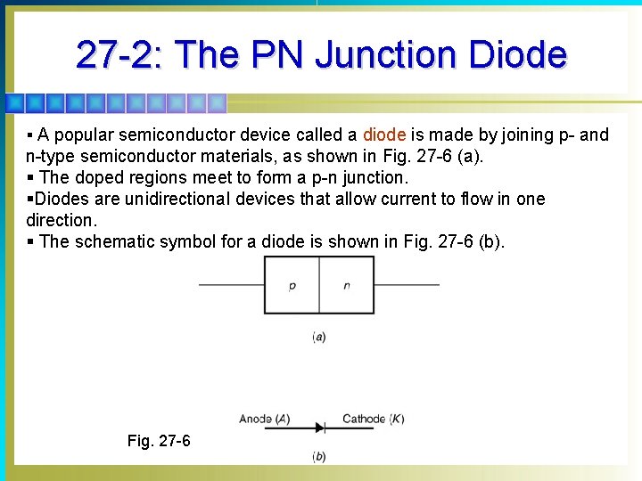
27 -2: The PN Junction Diode § A popular semiconductor device called a diode is made by joining p- and n-type semiconductor materials, as shown in Fig. 27 -6 (a). § The doped regions meet to form a p-n junction. §Diodes are unidirectional devices that allow current to flow in one direction. § The schematic symbol for a diode is shown in Fig. 27 -6 (b). Fig. 27 -6

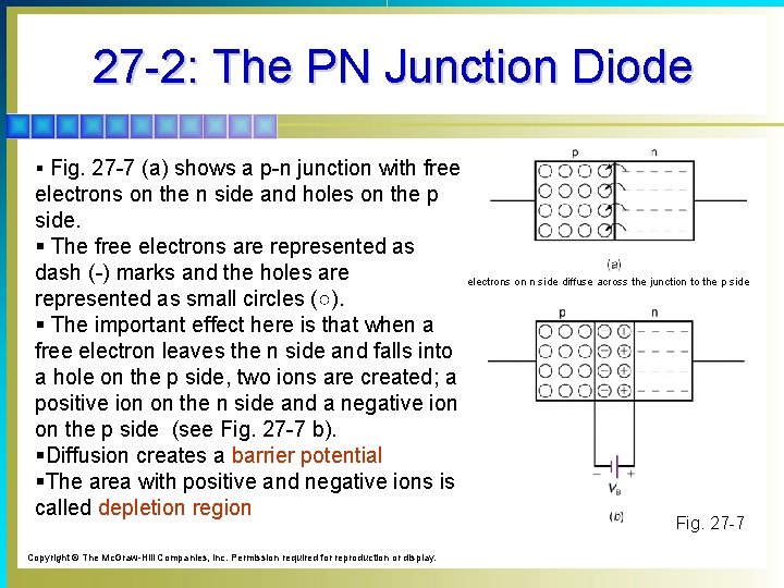
27 -2: The PN Junction Diode § Fig. 27 -7 (a) shows a p-n junction with free electrons on the n side and holes on the p side. § The free electrons are represented as dash (-) marks and the holes are represented as small circles (○). § The important effect here is that when a free electron leaves the n side and falls into a hole on the p side, two ions are created; a positive ion on the n side and a negative ion on the p side (see Fig. 27 -7 b). §Diffusion creates a barrier potential §The area with positive and negative ions is called depletion region Copyright © The Mc. Graw-Hill Companies, Inc. Permission required for reproduction or display. electrons on n side diffuse across the junction to the p side Fig. 27 -7

27 -2: The PN Junction Diode § The term bias voltage is defined as the DC voltage applied across the terminals of a PN junction §A PN junction is forward biased when a positive voltage is applied to the P-region with respect to the N-region §A PN junction is reversed-biased when the voltage polarity is reversed Copyright © The Mc. Graw-Hill Companies, Inc. Permission required for reproduction or display.

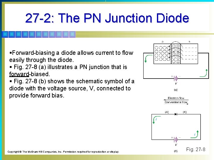
27 -2: The PN Junction Diode §Forward-biasing a diode allows current to flow easily through the diode. § Fig. 27 -8 (a) illustrates a PN junction that is forward-biased. § Fig. 27 -8 (b) shows the schematic symbol of a diode with the voltage source, V, connected to provide forward bias. Copyright © The Mc. Graw-Hill Companies, Inc. Permission required for reproduction or display. Fig. 27 -8

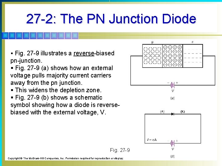
27 -2: The PN Junction Diode § Fig. 27 -9 illustrates a reverse-biased pn-junction. § Fig. 27 -9 (a) shows how an external voltage pulls majority current carriers away from the pn junction. § This widens the depletion zone. § Fig. 27 -9 (b) shows a schematic symbol showing how a diode is reversebiased with the external voltage, V. Fig. 27 -9 Copyright © The Mc. Graw-Hill Companies, Inc. Permission required for reproduction or display.

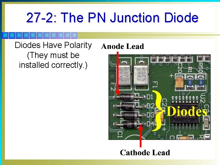
27 -2: The PN Junction Diodes Have Polarity (They must be installed correctly. )

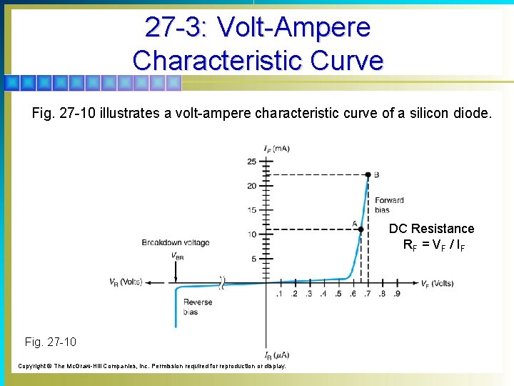
27 -3: Volt-Ampere Characteristic Curve § Figure 27 -10 (next slide) is a graph of diode current versus diode voltage for a silicon diode. § The graph includes the diode current for both forwardand reverse-bias voltages. § The upper right quadrant of the graph represents the forward-bias condition. § Beyond 0. 6 V of forward bias the diode current increases sharply. § The lower left quadrant of the graph represents the reverse-bias condition. § Only a small current flows until breakdown is reached.

27 -3: Volt-Ampere Characteristic Curve Fig. 27 -10 illustrates a volt-ampere characteristic curve of a silicon diode. DC Resistance RF = VF / IF Fig. 27 -10 Copyright © The Mc. Graw-Hill Companies, Inc. Permission required for reproduction or display.

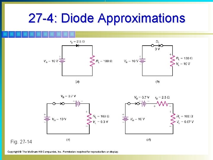
27 -4: Diode Approximations § Three different approximations can be used when analyzing diode circuits. § The one used depends on the desired accuracy of your circuit calculations. § These approximations are referred to as § The first approximation § The second approximation § The third approximation

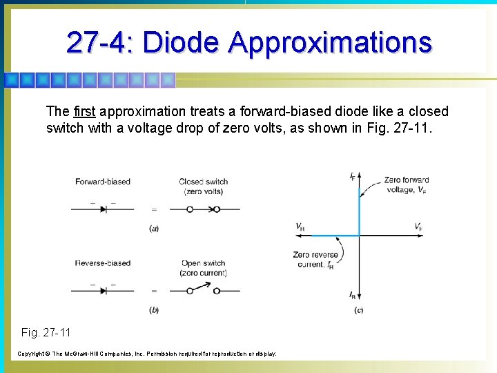
27 -4: Diode Approximations The first approximation treats a forward-biased diode like a closed switch with a voltage drop of zero volts, as shown in Fig. 27 -11 Copyright © The Mc. Graw-Hill Companies, Inc. Permission required for reproduction or display.

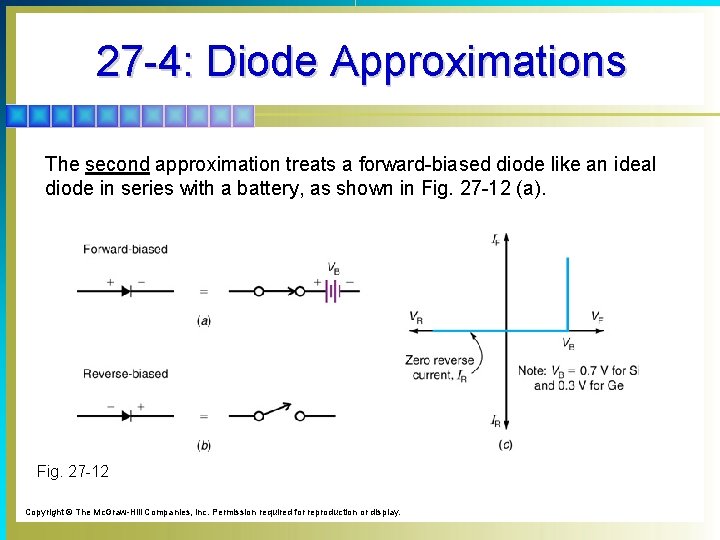
27 -4: Diode Approximations The second approximation treats a forward-biased diode like an ideal diode in series with a battery, as shown in Fig. 27 -12 (a). Fig. 27 -12 Copyright © The Mc. Graw-Hill Companies, Inc. Permission required for reproduction or display.

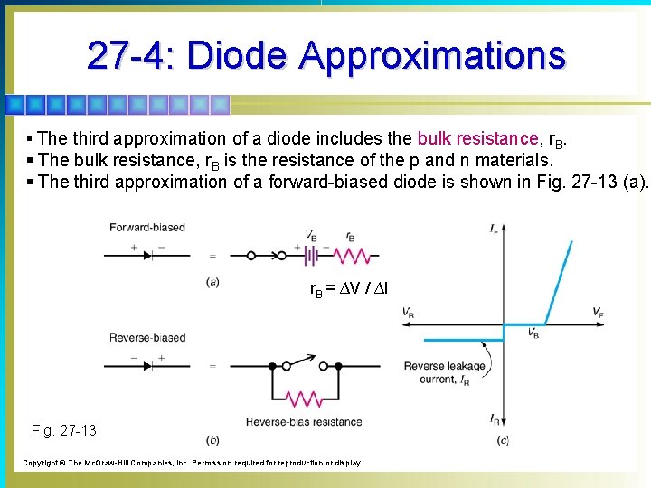
27 -4: Diode Approximations § The third approximation of a diode includes the bulk resistance, r. B. § The bulk resistance, r. B is the resistance of the p and n materials. § The third approximation of a forward-biased diode is shown in Fig. 27 -13 (a). r. B = ∆V / ∆I Fig. 27 -13 Copyright © The Mc. Graw-Hill Companies, Inc. Permission required for reproduction or display.

27 -4: Diode Approximations Fig. 27 -14 Copyright © The Mc. Graw-Hill Companies, Inc. Permission required for reproduction or display.

27 -5: Diode Ratings § Diode ratings include maximum ratings and electrical characteristics. § Typical ratings are § Breakdown Voltage Rating, VBR § Average Forward-Current rating, IO § Maximum Forward-Surge Current Rating, IFSM § Maximum Reverse Current, IR

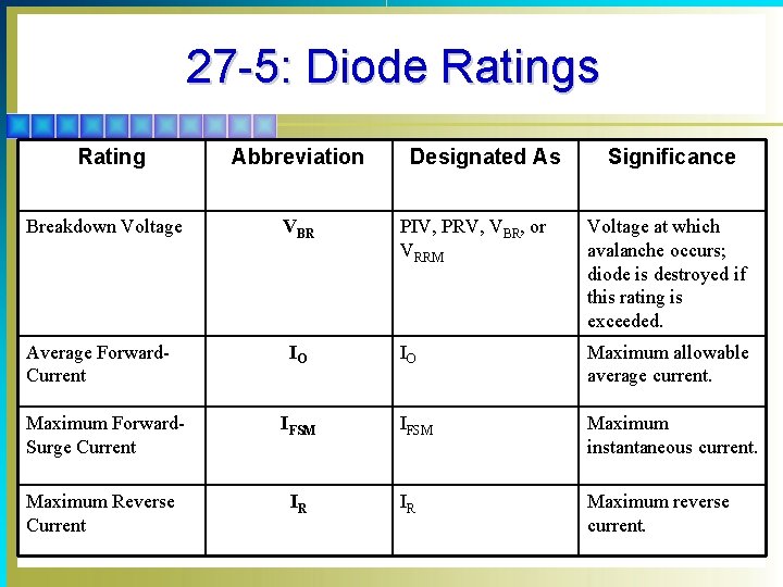
27 -5: Diode Ratings Rating Breakdown Voltage Average Forward. Current Abbreviation VBR IO Maximum Forward. Surge Current IFSM Maximum Reverse Current IR Designated As Significance PIV, PRV, VBR, or VRRM Voltage at which avalanche occurs; diode is destroyed if this rating is exceeded. IO Maximum allowable average current. IFSM Maximum instantaneous current. IR Maximum reverse current.

27 -6: Rectifier Diodes § A circuit that converts the ac power-line voltage to the required dc value is called a power supply. § The most important components in power supplies are rectifier diodes, which convert ac line voltage to dc voltage. § Diodes are able to produce a dc output voltage because they are unidirectional devices allowing current to flow through them in only one direction.

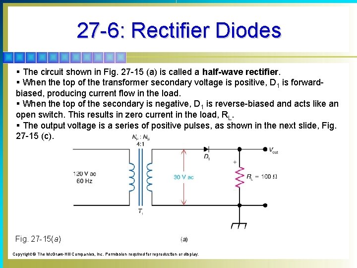
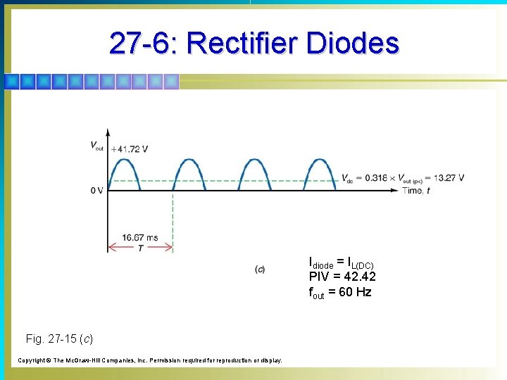
27 -6: Rectifier Diodes § The circuit shown in Fig. 27 -15 (a) is called a half-wave rectifier. § When the top of the transformer secondary voltage is positive, D 1 is forwardbiased, producing current flow in the load. § When the top of the secondary is negative, D 1 is reverse-biased and acts like an open switch. This results in zero current in the load, RL. § The output voltage is a series of positive pulses, as shown in the next slide, Fig. 27 -15 (c). Fig. 27 -15(a) Copyright © The Mc. Graw-Hill Companies, Inc. Permission required for reproduction or display.

27 -6: Rectifier Diodes Idiode = IL(DC) PIV = 42. 42 fout = 60 Hz Fig. 27 -15 (c) Copyright © The Mc. Graw-Hill Companies, Inc. Permission required for reproduction or display.

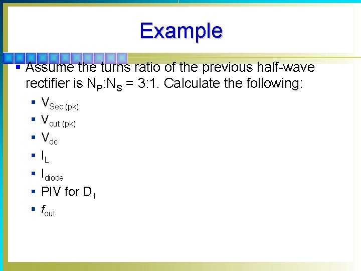
Example § Assume the turns ratio of the previous half-wave rectifier is NP: NS = 3: 1. Calculate the following: § VSec (pk) § Vout (pk) § § § Vdc IL Idiode PIV for D 1 fout

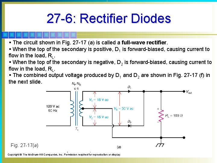
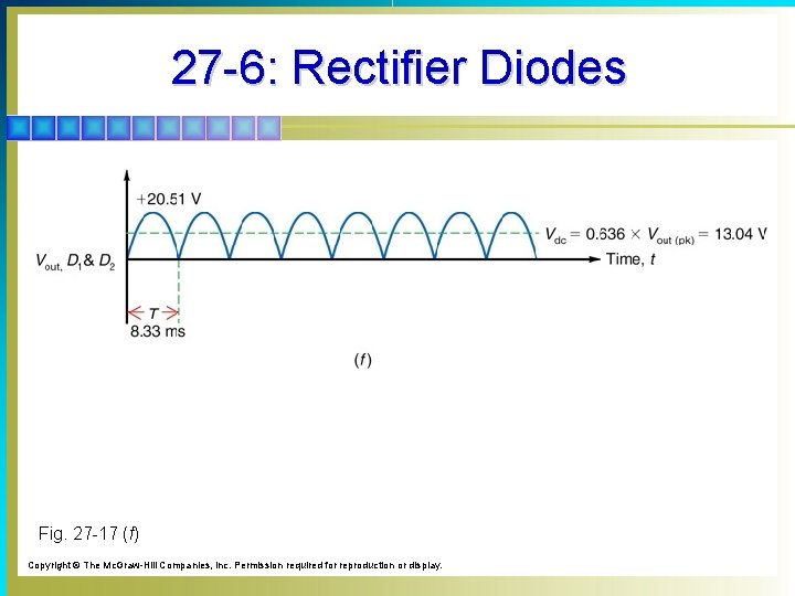
27 -6: Rectifier Diodes § The circuit shown in Fig. 27 -17 (a) is called a full-wave rectifier. § When the top of the secondary is positive, D 1 is forward-biased, causing current to flow in the load, RL. § When the top of the secondary is negative, D 2 is forward-biased, causing current to flow in the load, RL. § The combined output voltage produced by D 1 and D 2 are shown in Fig. 27 -17 (f) in the next slide. Fig. 27 -17(a) Copyright © The Mc. Graw-Hill Companies, Inc. Permission required for reproduction or display.

27 -6: Rectifier Diodes Fig. 27 -17 (f) Copyright © The Mc. Graw-Hill Companies, Inc. Permission required for reproduction or display.

Example § Assume the turns ratio of the previous full-wave rectifier is NP: NS = 3: 1. Calculate the following using the second approximation: § VSec (pk) § Vout (pk) § § § Vdc IL Idiode PIV for D 1 fout

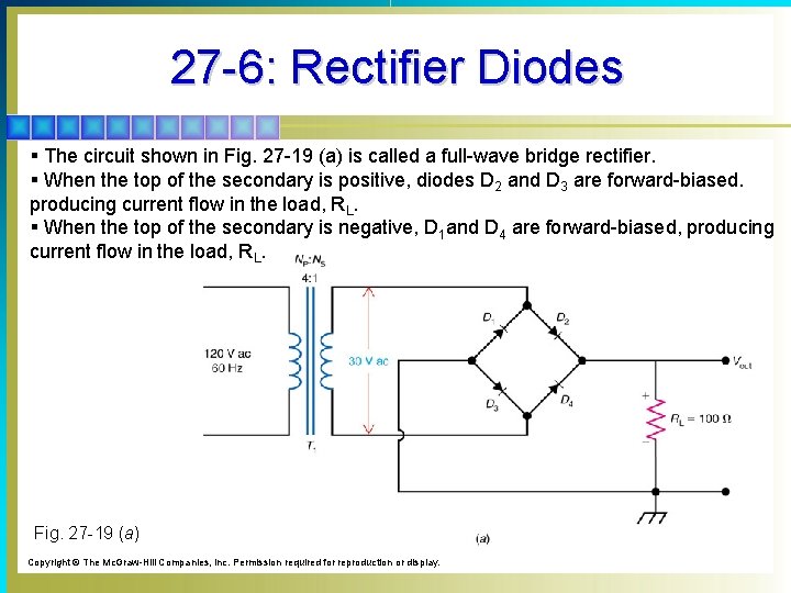
27 -6: Rectifier Diodes § The circuit shown in Fig. 27 -19 (a) is called a full-wave bridge rectifier. § When the top of the secondary is positive, diodes D 2 and D 3 are forward-biased. producing current flow in the load, RL. § When the top of the secondary is negative, D 1 and D 4 are forward-biased, producing current flow in the load, RL. Fig. 27 -19 (a) Copyright © The Mc. Graw-Hill Companies, Inc. Permission required for reproduction or display.

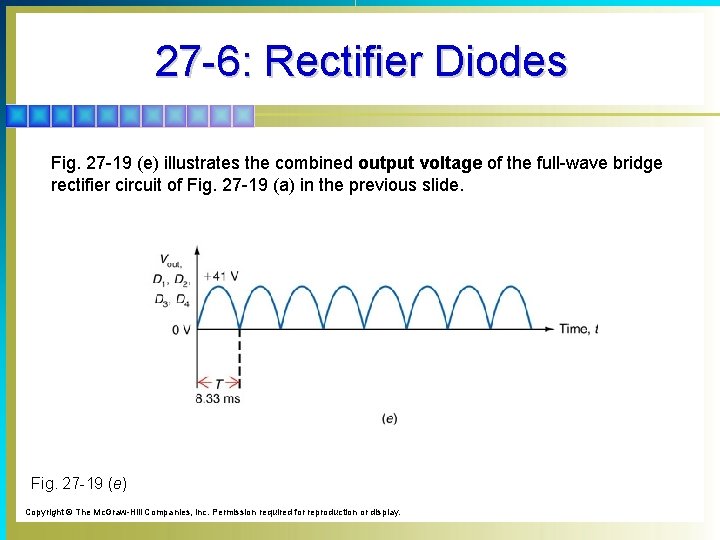
27 -6: Rectifier Diodes Fig. 27 -19 (e) illustrates the combined output voltage of the full-wave bridge rectifier circuit of Fig. 27 -19 (a) in the previous slide. Fig. 27 -19 (e) Copyright © The Mc. Graw-Hill Companies, Inc. Permission required for reproduction or display.

Example § Assume the turns ratio of the previous full-wave bridge rectifier is NP: NS = 3: 1. Calculate the following: § VS § Vdc § IL § Idiode § PIV for each diode § fout

27 -7: Special Diodes § Besides rectification, a semiconductor diode has many other useful applications. § Semiconductor diodes can be manufactured to regulate voltage or emit different colors of light. § Examples of two special purpose diodes are § Light-emitting diode § Zener diode

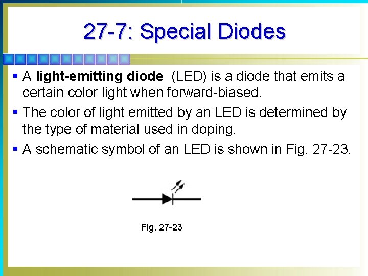
27 -7: Special Diodes § A light-emitting diode (LED) is a diode that emits a certain color light when forward-biased. § The color of light emitted by an LED is determined by the type of material used in doping. § A schematic symbol of an LED is shown in Fig. 27 -23

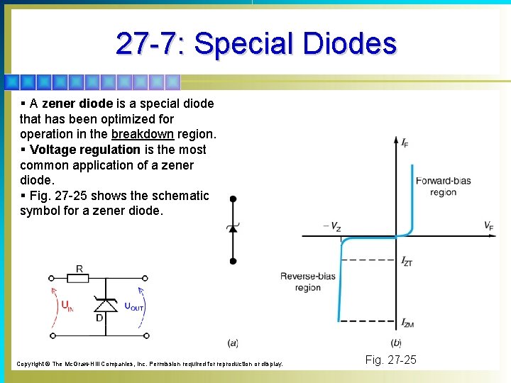
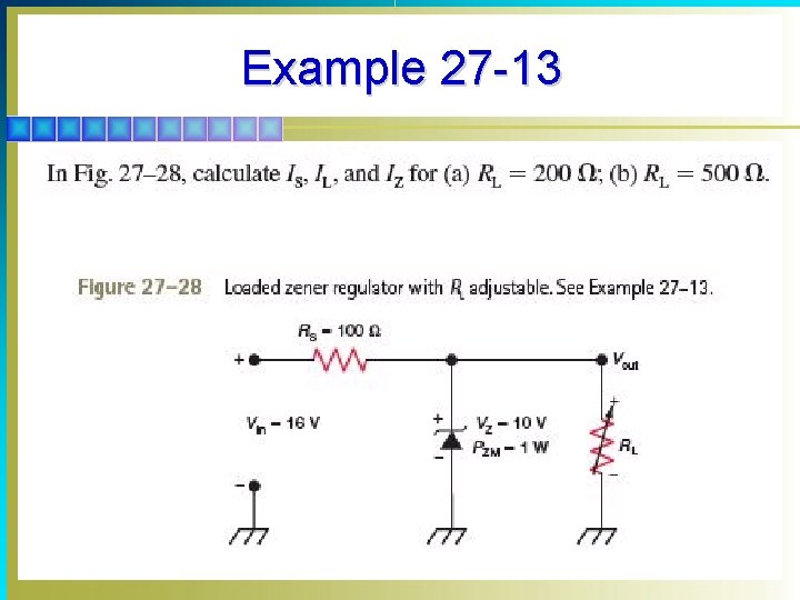
27 -7: Special Diodes § A zener diode is a special diode that has been optimized for operation in the breakdown region. § Voltage regulation is the most common application of a zener diode. § Fig. 27 -25 shows the schematic symbol for a zener diode. Copyright © The Mc. Graw-Hill Companies, Inc. Permission required for reproduction or display. Fig. 27 -25

Example 27 -13

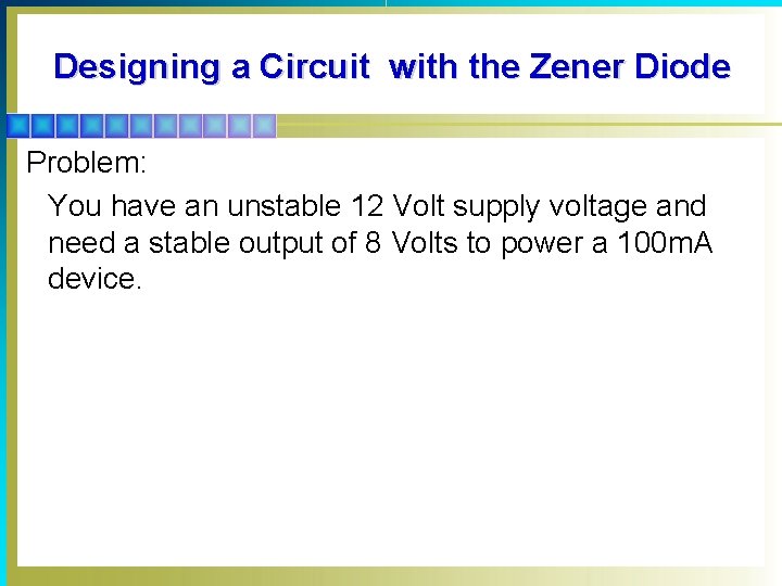
Designing a Circuit with the Zener Diode Problem: You have an unstable 12 Volt supply voltage and need a stable output of 8 Volts to power a 100 m. A device.

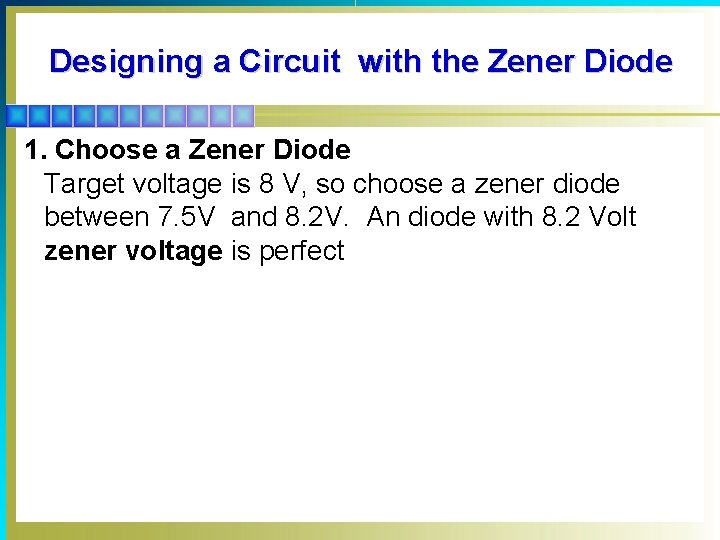
Designing a Circuit with the Zener Diode 1. Choose a Zener Diode Target voltage is 8 V, so choose a zener diode between 7. 5 V and 8. 2 V. An diode with 8. 2 Volt zener voltage is perfect

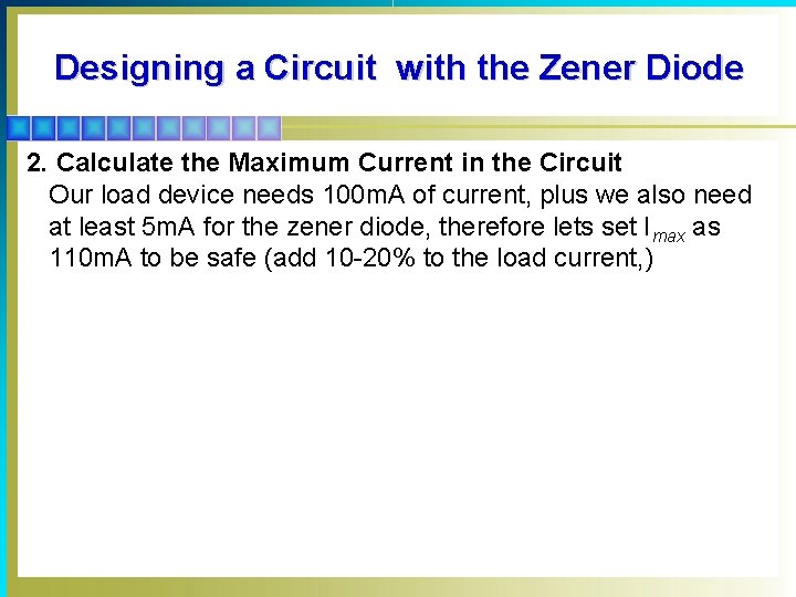
Designing a Circuit with the Zener Diode 2. Calculate the Maximum Current in the Circuit Our load device needs 100 m. A of current, plus we also need at least 5 m. A for the zener diode, therefore lets set Imax as 110 m. A to be safe (add 10 -20% to the load current, )

Designing a Circuit with the Zener Diode 3. Select the Power Rating of the Zener Diode If a large current flows through a small zener diode it will be destroyed, therefore we calculate the power to be lost in the diode and select a diode rated above that value. zener power rating = 8. 2 * 0. 110 = 0. 9 Watts. Because, no current is flowing through the load when the device is switched off. Therefore a 1. 3 Watt power rated zener diode should be perfect.

Designing a Circuit with the Zener Diode 4. Select the Resistor The voltage dropped across the resistor is equal to the difference between the source voltage and the zener voltage = 12 -8 = 4 Volts, and therefore the resistance according to Ohm's Law is the voltage drop divided by Imax = 4/0. 110 = 36 Ohms so choose a 39 Ohm resistor. If the source voltage is likely to be much over the 12 Volts stated then the voltage dropped across the resistor will be larger and so a resistor with a larger resistance may be required.

Designing a Circuit with the Zener Diode 5. Select the Power Rating of the Resistor The power dissipated in the resistor is equal to the voltage drop across the resistor multiplied by Imax. Therefore in this example power = 4 * 0. 110 = 0. 440 Watts. Using a 0. 5 Watt resistor would be cutting it a bit fine - particularly if the source voltage is going to fluctuate higher regularly, therefore a 1 or 2 Watt rated resistor should be used here despite it costing a few pennies extra.