William Stallings Computer Organization and Architecture 6 th
")


 • Sequential (循序的) —Start at the beginning and read through in")
 • Random —Individual addresses identify(確認) locations exactly —Access time is independent")
 —Time between presenting the address and getting the")
 • Non-random-access memory N TN = TA")

 Volatility (揮發性) Erasable Power consumption")


 of Reference (參考) • During the course of the execution of a")


 —Cache block of 4")


 (j ) 0 m 1 m+1")


 bits • Number of")


 bits Number")
")


 •")
 bits Number")

 Direct mapping • No choice • Each block only maps to")
 Associative & Set Associative • • • Hardware implemented(實行) algorithm (speed)")


 • Bus watching with write through — Each cache controller monitor")


")


- Slides: 58
William Stallings Computer Organization and Architecture 6 th Edition Chapter 4 Cache Memory (快取,快速緩衝貯存區)
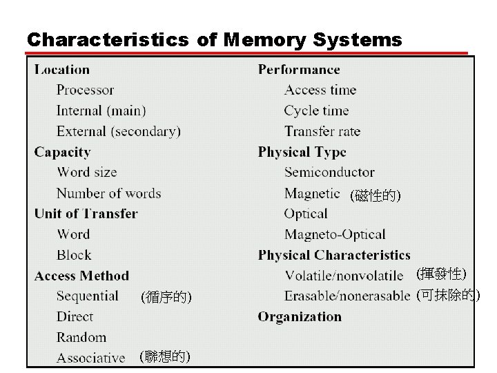
Location • CPU — Registers, Control Memory • Internal —Cache —Main Memory • External — Disk, Tape, …
Capacity • Word size —The natural unit of organisation —Number of bits to represent a number —Instruction length • Number of words —or Bytes (External)
Unit of Transfer • Internal —Usually governed by data bus width • External —Usually a block which is much larger than a word • Addressable unit 唯一地 —Smallest location which can be uniquely addressed —Word internally A: Length of an address (in bits) —Cluster on disks N: Number of addressable units 叢、群 A N=2
Access Methods (1) • Sequential (循序的) —Start at the beginning and read through in order —Access time depends on location of data and previous location —e. g. tape • Direct —Individual blocks have unique address —Access is by jumping to vicinity plus sequential search 附近 —Access time depends on location and previous location —e. g. disk
Access Methods (2) • Random —Individual addresses identify(確認) locations exactly —Access time is independent of location or previous access —e. g. RAM (Random Access Memory) • Associative (聯想的) —Data is located by a comparison with contents of a portion of the store —A word is retrieved (取回) based on a portion of its contents rather than its address —Access time is independent of location or previous access —e. g. cache
Performance • Access time (latency 潛伏、遲延) —Time between presenting the address and getting the valid data (RAM) —Time it takes to position the read-write mechanism at the desired location (non-random-access memory) • Memory Cycle time —Time may be required for the memory to “recover” (eg. destructively read) before next access —Cycle time is access + recovery • Transfer Rate —Rate at which data can be moved
Transfer Rate • RAM — 1/(cycle time) • Non-random-access memory N TN = TA + — R TN TA N R = = Average time to read or write N bits Average access time Number of bits Transfer rate (bps)
Physical Types • Semiconductor —RAM • Magnetic —Disk & Tape • Optical —CD & DVD • Others —Bubble (磁泡) —Holographic (Optical 3 D storage)
Physical Characteristics • • Decay (衰減) Volatility (揮發性) Erasable Power consumption
Organization • Physical arrangement of bits into words • Not always obvious • e. g. interleaved (交錯)
Memory Hierarchy • Registers —In CPU • Internal or Main memory —May include one or more levels of cache —“RAM” • External memory —Backing store
Memory Hierarchy - Diagram MO: Magneto Optical WORM: Write Once, Read Many
The Bottom Line • How much? —Capacity • How fast? —Time is money • How expensive?
Hierarchy List • • Registers L 1 Cache L 2 Cache Main memory Disk cache Disk Optical Tape
So you want fast? • It is possible to build a computer which uses only static RAM (see later) • This would be very fast • This would need no cache —How can you cache? • This would cost a very large amount
Locality (位置) of Reference (參考) • During the course of the execution of a program, memory references tend to cluster • e. g. loops • Spatial (空間的) Locality Page 129 — The tendency (傾向) of execution to involve (包括) a number of memory locations that are clustered • Temporal (暫時的) Locality — The tendency for a processor to access memory locations that have been used recently. Appendix 4 A
Cache • Small amount of fast memory • Sits between normal main memory and CPU • May be located on CPU chip or module
Cache/Main Memory Structure 1 Block = K words Memory: 2 n words, M Blocks (M = 2 n/K) Cache: C Blocks (Lines) C << M
Cache operation - Overview • • CPU requests contents of memory location Check cache for this data If present, get from cache (fast) If not present, read required block from main memory to cache • Then deliver from cache to CPU • Cache includes tags to identify which block of main memory is in each cache slot (槽)
Cache Read Operation - Flowchart
Cache Design
Size does matter • Cost —More cache is expensive • Speed —More cache is faster (up to a point) —Checking cache for data takes time
Typical Cache Organization
Mapping Function • Example: —Cache of 64 KByte (216 bytes) —Cache block of 4 bytes – i. e. cache is 16 k (214) lines of 4 bytes —Main memory: 16 MBytes – 24 bit address (224=16 M) 1 KBytes = 210 bytes 1 MBytes = 220 bytes 1 GBytes = 230 bytes
Direct Mapping • Each block of main memory maps to only one cache line —i. e. if a block is in cache, it must be in one specific place • • Address is in two parts (Significant: 顯著的) Least Significant w bits identify unique word Most Significant s bits specify one memory block The MSBs are split into a cache line field r and a tag of s-r (most significant) s bits w bits s-r bits w bits tag line # word #
Direct Mapping Address Structure Tag s-r 8 Line or Slot r Word w 14 • 24 bit address • 2 bit word identifier (4 byte block) • 22 bit block identifier — 8 bit tag (=22 -14) — 14 bit slot or line (214 lines in cache) • No two blocks in the same line have the same Tag field • Check contents of cache by finding line and checking Tag 2
Direct Mapping Cache Line Table Cache line (i) (j ) 0 m 1 m+1 Main Memory blocks held 0, m, 2 m, … 2 s- 1, m+1, 2 m+1, … 2 s- i =m-1 j modulo m , where m is 2 m-1, the number in cache m-1, 3 m-1, of…lines 2 s-1 modulo (以. . . 為模) 17 mod 6 = 5 20 mod 8 = 4
Direct Mapping Cache Organization 1 2 4‘ 3 4
Direct Mapping Example
Direct Mapping Summary • Address length = (s + w) bits • Number of addressable units = 2 s+w words or bytes • Block size = line size = 2 w words or bytes • Number of blocks in main memory = 2 s+w/2 w = 2 s • Number of lines in cache = m = 2 r • Size of tag = (s – r) bits
Direct Mapping pros & cons • Simple • Inexpensive • Fixed location for given block —If a program accesses 2 blocks that map to the same line repeatedly, cache misses are very high
Associative Mapping • A main memory block can load into any line of cache • Memory address is interpreted as tag and word • Tag uniquely identifies block of memory • Every line’s tag is examined for a match • Cache searching gets expensive
Fully Associative Cache Organization 1 2 2‘
Associative Mapping Example 3 9 C 0011100 E 7
Associative Mapping Address Structure Tag 22 bit Word 2 bit • 22 bit tag stored with each 32 bit block of data • Compare tag field with tag entry in cache to check for hit • Least significant 2 bits of address identify which word is required from 32 bit data block • e. g. —Address Tag —FFFFFC 3 FFFFF related Data 2468 * not related Cache line 3 FFF
Associative Mapping Summary • • • Address length = (s + w) bits Number of addressable units = 2 s+w words or bytes Block size = line size = 2 w words or bytes Number of blocks in main memory = 2 s+ w/2 w = 2 s Number of lines in cache = undetermined (未確定的) Size of tag = s bits (not determined by address format)
Set Associative Mapping • Cache is divided into a number of sets (v sets) • Each set contains a number of lines ( k lines) m = v k, where m is the number of lines in cache • A given block maps to any line in a given set — e. g. Block j can be in any line of set i i = j modulo v • e. g. 2 (k) lines per set — 2 (k) way associative mapping —A given block can be in one of 2 (k) lines in only one set
Two Way Set Associative Cache Organization v = 2 d 1 3‘ 2 3
Set Associative Mapping Address Structure Tag 9 bit Word 2 bit Set 13 bit • Use set field to determine cache set to look in • Compare tag field to see if we have a hit • e. g —Address — 1 FF 7 FFC — 001 7 FFC Tag 1 FF 001 Data 12345678 11223344 related Set number 1 FFF
Two Way Set Associative Mapping Example
Set Associative Mapping Example • 13 bit set number (i. e. 213 sets) • Block number in main memory is modulo 213 • 000000, 008000, …, FF 8000 map to set 0
Set Associative Mapping Summary • • Address length = (s + w) bits Number of addressable units = 2 s+w words or bytes Block size = line size = 2 w words or bytes Number of blocks in main memory = 2 s Number of lines in set = k Number of sets = v = 2 d Number of lines in cache = kv = k * 2 d Size of tag = (s – d) bits
Assignment 2 • Cache size: 512 KBytes • Cache block size: 32 Bytes • Main memory size: 2 GBytes • What is the address format of — Direct Mapping — Fully Associative — 4 -way Associative
Replacement Algorithms (1) Direct mapping • No choice • Each block only maps to one line • Replace that line
Replacement Algorithms (2) Associative & Set Associative • • • Hardware implemented(實行) algorithm (speed) Least Recently used (LRU) best hit ratio e. g. in 2 way set associative —Which of the 2 block is lru? (USE bit per line) • First in first out (FIFO) —replace block that has been in cache longest • Least frequently used (LFU) (use counters) —replace block which has had fewest hits • Random
Write Policy • Must not overwrite a cache block unless main memory is up to date • Multiple CPUs may have individual caches • I/O may address main memory directly
Write through • All writes go to main memory as well as cache • Multiple CPUs can monitor main memory traffic to keep local (to CPU) cache up to date • Lots of traffic • Slows down writes
Write back • Updates initially made in cache only • Update bit for cache slot is set when update occurs • If block is to be replaced, write to main memory only if update bit is set • Other caches get out of sync • I/O must access main memory through cache • 15% of memory references are writes
Cache Coherency (一致性) • Bus watching with write through — Each cache controller monitor the bus. • Hardware Transparency (透通性) — use additional hardware to ensure that all updates to main memory via cache are reflected in all caches. • Noncacheable Memory —Only a portion of main memory (noncacheable) is shared by more than one processor.
Other Issues • Line Size —By principle of locality, the hit ratio at first increases when the block size increases. —When the block size becomes even bigger, the hit ratio begin to decrease. • Number of Caches —Multilevel Caches – On-chip cache (L 1) – Off-chip (external) cache (L 2) —Unified vs. Split Caches – Data cache / Instruction cache
Pentium 4 Cache • 80386 – no on chip cache • 80486 – 8 k using 16 byte lines and four way set associative organization • Pentium (all versions) – two on chip L 1 caches — Data & instructions • Pentium 4 – L 1 data caches — 8 k bytes — 64 byte lines — four way set associative • L 2 cache — Feeding both L 1 caches — 256 k — 128 byte lines — 8 way set associative
Pentium 4 Diagram (Simplified)
Pentium 4 Core Processor • Fetch/Decode Unit — Fetches instructions from L 2 cache — Decode into micro-ops — Store micro-ops in L 1 cache • Out of order execution logic — Schedules micro-ops — Based on data dependence and resources — May speculatively execute • Execution units — Execute micro-ops — Data from L 1 cache — Results in registers • Memory subsystem — L 2 cache and systems bus
Pentium 4 Design Reasoning • Decodes instructions into RISC like micro-ops before L 1 cache • Micro-ops fixed length — Superscalar pipelining and scheduling • Pentium instructions long & complex • Performance improved by separating decoding from scheduling & pipelining — (More later – ch 14) • Data cache is write back — Can be configured to write through • L 1 cache controlled by 2 bits in register — CD = cache disable — NW = not write through — 2 instructions to invalidate (flush) cache and write back then invalidate
Comparison of Cache Sizes
Itanium