VLSI Testing Lecture 16 RF Testing I Dr
- Slides: 28

VLSI Testing Lecture 16: RF Testing I Dr. Vishwani D. Agrawal James J. Danaher Professor of Electrical and Computer Engineering Auburn University, Alabama 36849, USA vagrawal@eng. auburn. edu http: //www. eng. auburn. edu/~vagrawal IIT Delhi, Aug 27, 2013, 2: 30 -4: 30 PM Copyright 2008, Agrawal Lectures 16: RF Testing 1

References 1. S. Bhattacharya and A. Chatterjee, "RF Testing, " Chapter 16, pages 2. 3. 4. 5. 6. 745 -789, in System on Chip Test Architectures, edited by L. -T. Wang, C. E. Stroud and N. A. Touba, Amsterdam: Morgan-Kaufman, 2008. M. L. Bushnell and V. D. Agrawal, Essentials of Electronic Testing for Digital, Memory & Mixed-Signal VLSI Circuits, Boston: Springer, 2000. J. Kelly and M. Engelhardt, Advanced Production Testing of RF, So. C, and Si. P Devices, Boston: Artech House, 2007. B. Razavi, RF Microelectronics, Upper Saddle River, New Jersey: Prentice Hall PTR, 1998. J. Rogers, C. Plett and F. Dai, Integrated Circuit Design for High. Speed Frequency Synthesis, Boston: Artech House, 2006. K. B. Schaub and J. Kelly, Production Testing of RF and System-on-achip Devices for Wireless Communications, Boston: Artech House, 2004. Copyright 2008, Agrawal Lectures 16: RF Testing 2

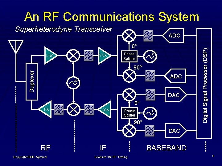
An RF Communications System Superheterodyne Transceiver 0° VGA LNA Phase Splitter LO Duplexer 90° ADC LO DAC 0° PA VGA Phase Splitter LO 90° Digital Signal Processor (DSP) ADC DAC RF Copyright 2008, Agrawal IF Lectures 16: RF Testing BASEBAND 3

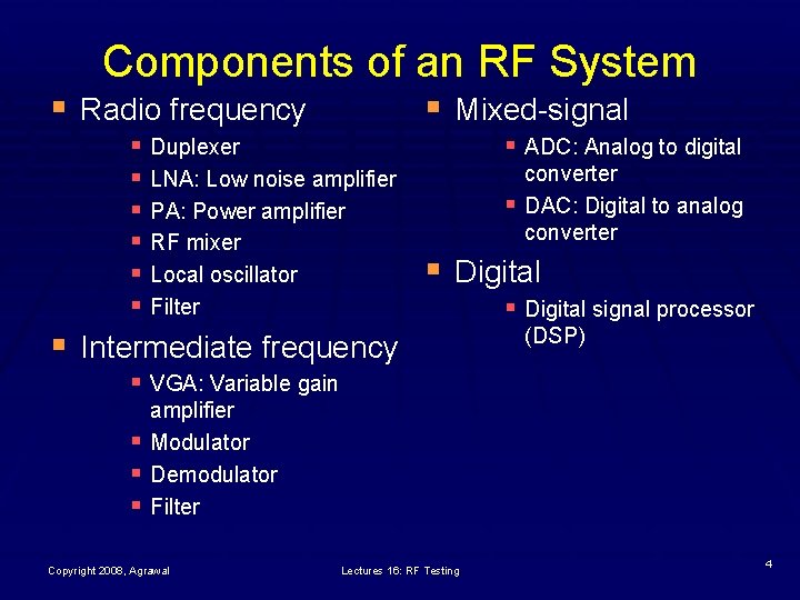
Components of an RF System § Radio frequency § Mixed-signal § Duplexer § LNA: Low noise amplifier § PA: Power amplifier § RF mixer § Local oscillator § Filter § ADC: Analog to digital converter § DAC: Digital to analog converter § Digital § Intermediate frequency § Digital signal processor (DSP) § VGA: Variable gain amplifier § Modulator § Demodulator § Filter Copyright 2008, Agrawal Lectures 16: RF Testing 4

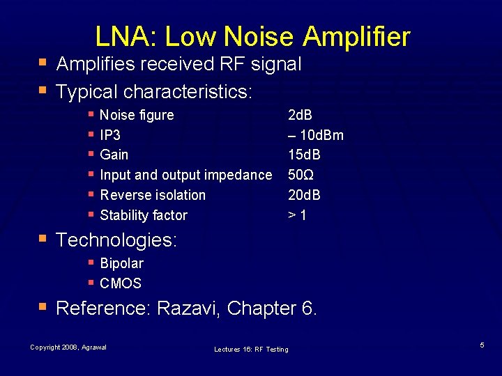
LNA: Low Noise Amplifier § Amplifies received RF signal § Typical characteristics: § Noise figure § IP 3 § Gain § Input and output impedance § Reverse isolation § Stability factor 2 d. B – 10 d. Bm 15 d. B 50Ω 20 d. B >1 § Technologies: § Bipolar § CMOS § Reference: Razavi, Chapter 6. Copyright 2008, Agrawal Lectures 16: RF Testing 5

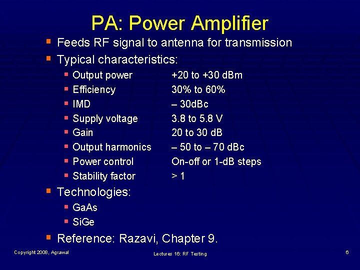
PA: Power Amplifier § Feeds RF signal to antenna for transmission § Typical characteristics: § § § Output power +20 to +30 d. Bm § Efficiency 30% to 60% § IMD – 30 d. Bc § Supply voltage 3. 8 to 5. 8 V § Gain 20 to 30 d. B § Output harmonics – 50 to – 70 d. Bc § Power control On-off or 1 -d. B steps § Stability factor >1 Technologies: § Ga. As § Si. Ge Reference: Razavi, Chapter 9. Copyright 2008, Agrawal Lectures 16: RF Testing 6

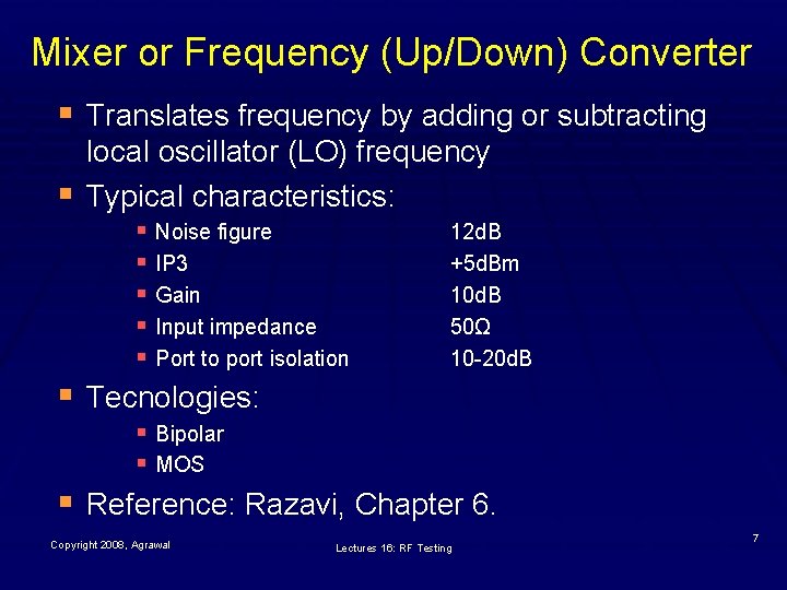
Mixer or Frequency (Up/Down) Converter § Translates frequency by adding or subtracting § local oscillator (LO) frequency Typical characteristics: § Noise figure § IP 3 § Gain § Input impedance § Port to port isolation 12 d. B +5 d. Bm 10 d. B 50Ω 10 -20 d. B § Tecnologies: § Bipolar § MOS § Reference: Razavi, Chapter 6. Copyright 2008, Agrawal Lectures 16: RF Testing 7

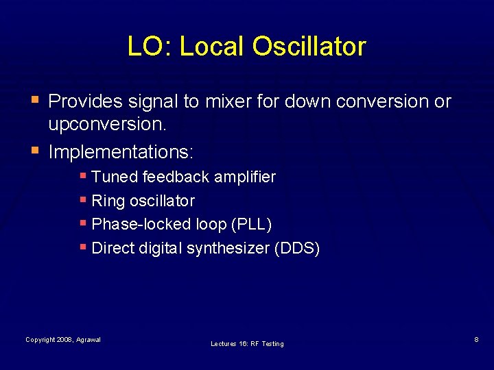
LO: Local Oscillator § Provides signal to mixer for down conversion or § upconversion. Implementations: § Tuned feedback amplifier § Ring oscillator § Phase-locked loop (PLL) § Direct digital synthesizer (DDS) Copyright 2008, Agrawal Lectures 16: RF Testing 8

SOC: System-on-a-Chip § All components of a system are implemented on § § the same VLSI chip. Requires same technology (usually CMOS) used for all components. Components not implemented on present-day SOC: § Antenna § Power amplifier (PA) Copyright 2008, Agrawal Lectures 16: RF Testing 9

RF Tests § Basic tests § § § Scattering parameters (S-parameters) § Frequency and gain measurements § Power efficiency measurements Distortion measurements Noise measurements Copyright 2008, Agrawal Lectures 16: RF Testing 10

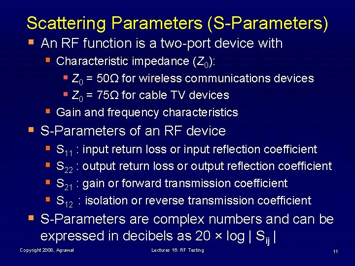
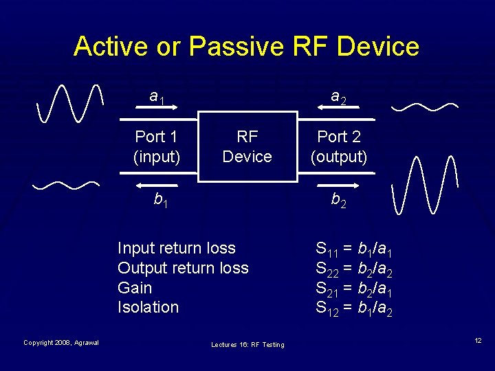
Scattering Parameters (S-Parameters) § An RF function is a two-port device with § Characteristic impedance (Z 0): § Z 0 = 50Ω for wireless communications devices § Z 0 = 75Ω for cable TV devices § Gain and frequency characteristics § S-Parameters of an RF device § S 11 : input return loss or input reflection coefficient § S 22 : output return loss or output reflection coefficient § S 21 : gain or forward transmission coefficient § S 12 : isolation or reverse transmission coefficient § S-Parameters are complex numbers and can be expressed in decibels as 20 × log | Sij | Copyright 2008, Agrawal Lectures 16: RF Testing 11

Active or Passive RF Device a 1 Port 1 (input) a 2 RF Device b 1 b 2 Input return loss Output return loss Gain Isolation Copyright 2008, Agrawal Port 2 (output) Lectures 16: RF Testing S 11 = b 1/a 1 S 22 = b 2/a 2 S 21 = b 2/a 1 S 12 = b 1/a 2 12

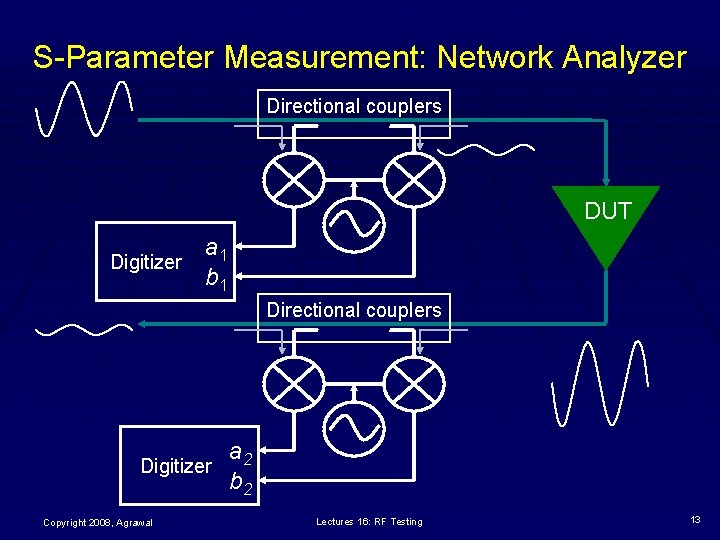
S-Parameter Measurement: Network Analyzer Directional couplers DUT a 1 Digitizer b 1 Directional couplers a 2 Digitizer b 2 Copyright 2008, Agrawal Lectures 16: RF Testing 13

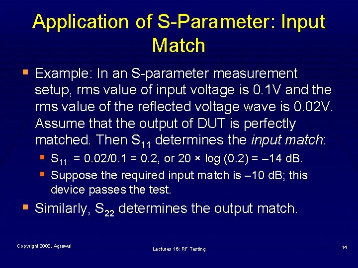
Application of S-Parameter: Input Match § Example: In an S-parameter measurement setup, rms value of input voltage is 0. 1 V and the rms value of the reflected voltage wave is 0. 02 V. Assume that the output of DUT is perfectly matched. Then S 11 determines the input match: § S 11 = 0. 02/0. 1 = 0. 2, or 20 × log (0. 2) = – 14 d. B. § Suppose the required input match is – 10 d. B; this device passes the test. § Similarly, S 22 determines the output match. Copyright 2008, Agrawal Lectures 16: RF Testing 14

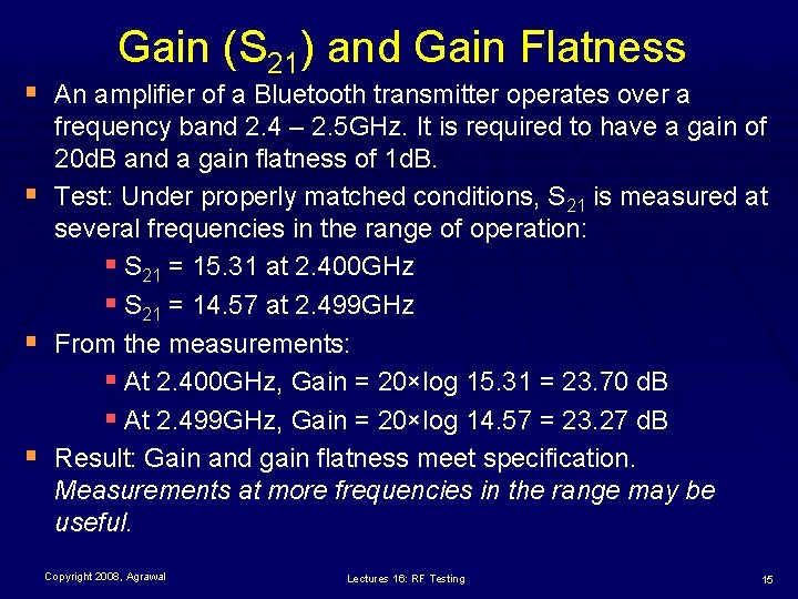
Gain (S 21) and Gain Flatness § An amplifier of a Bluetooth transmitter operates over a § § § frequency band 2. 4 – 2. 5 GHz. It is required to have a gain of 20 d. B and a gain flatness of 1 d. B. Test: Under properly matched conditions, S 21 is measured at several frequencies in the range of operation: § S 21 = 15. 31 at 2. 400 GHz § S 21 = 14. 57 at 2. 499 GHz From the measurements: § At 2. 400 GHz, Gain = 20×log 15. 31 = 23. 70 d. B § At 2. 499 GHz, Gain = 20×log 14. 57 = 23. 27 d. B Result: Gain and gain flatness meet specification. Measurements at more frequencies in the range may be useful. Copyright 2008, Agrawal Lectures 16: RF Testing 15

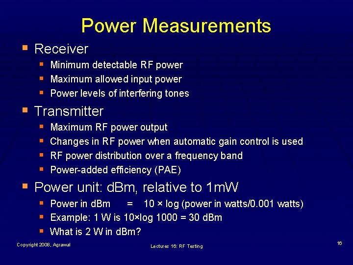
Power Measurements § Receiver § § § Minimum detectable RF power Maximum allowed input power Power levels of interfering tones § Transmitter § § Maximum RF power output Changes in RF power when automatic gain control is used RF power distribution over a frequency band Power-added efficiency (PAE) § Power unit: d. Bm, relative to 1 m. W § § § Power in d. Bm = 10 × log (power in watts/0. 001 watts) Example: 1 W is 10×log 1000 = 30 d. Bm What is 2 W in d. Bm? Copyright 2008, Agrawal Lectures 16: RF Testing 16

Harmonic Measurements § Multiples of the carrier frequency are called § § harmonics. Harmonics are generated due to nonlinearity in semiconductor devices and clipping (saturation) in amplifiers. Harmonics may interfere with other signals and must be measured to verify that a manufactured device meets the specification. Copyright 2008, Agrawal Lectures 16: RF Testing 17

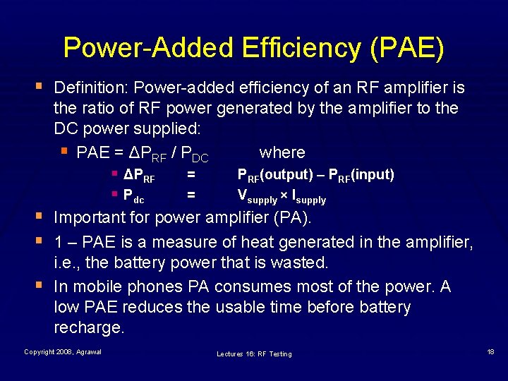
Power-Added Efficiency (PAE) § Definition: Power-added efficiency of an RF amplifier is § § § the ratio of RF power generated by the amplifier to the DC power supplied: § PAE = ΔPRF / PDC where § ΔPRF = PRF(output) – PRF(input) § Pdc = Vsupply × Isupply Important for power amplifier (PA). 1 – PAE is a measure of heat generated in the amplifier, i. e. , the battery power that is wasted. In mobile phones PA consumes most of the power. A low PAE reduces the usable time before battery recharge. Copyright 2008, Agrawal Lectures 16: RF Testing 18

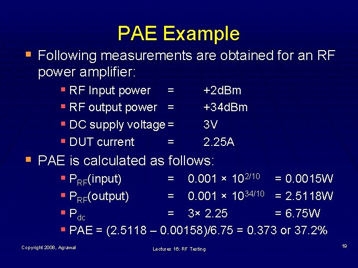
PAE Example § Following measurements are obtained for an RF § power amplifier: § RF Input power = +2 d. Bm § RF output power = +34 d. Bm § DC supply voltage = 3 V § DUT current = 2. 25 A PAE is calculated as follows: § PRF(input) = 0. 001 × 102/10 = 0. 0015 W § PRF(output) = 0. 001 × 1034/10 = 2. 5118 W § Pdc = 3× 2. 25 = 6. 75 W § PAE = (2. 5118 – 0. 00158)/6. 75 = 0. 373 or 37. 2% Copyright 2008, Agrawal Lectures 16: RF Testing 19

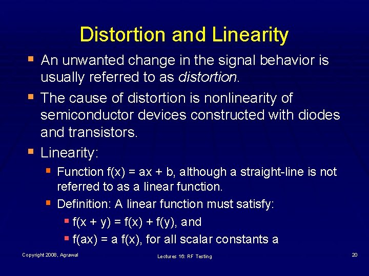
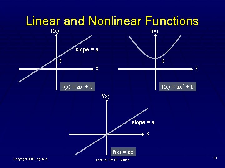
Distortion and Linearity § An unwanted change in the signal behavior is § § usually referred to as distortion. The cause of distortion is nonlinearity of semiconductor devices constructed with diodes and transistors. Linearity: § Function f(x) = ax + b, although a straight-line is not § referred to as a linear function. Definition: A linear function must satisfy: § f(x + y) = f(x) + f(y), and § f(ax) = a f(x), for all scalar constants a Copyright 2008, Agrawal Lectures 16: RF Testing 20

Linear and Nonlinear Functions f(x) slope = a b b x x f(x) = ax + b f(x) = ax 2 + b f(x) slope = a x f(x) = ax Copyright 2008, Agrawal Lectures 16: RF Testing 21

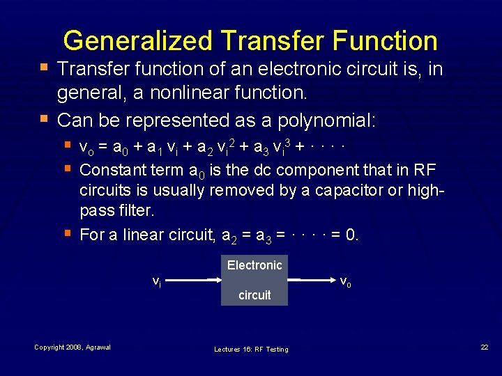
Generalized Transfer Function § Transfer function of an electronic circuit is, in § general, a nonlinear function. Can be represented as a polynomial: § vo = a 0 + a 1 vi + a 2 vi 2 + a 3 vi 3 + · · § Constant term a 0 is the dc component that in RF § circuits is usually removed by a capacitor or highpass filter. For a linear circuit, a 2 = a 3 = · · = 0. Electronic vi Copyright 2008, Agrawal circuit Lectures 16: RF Testing vo 22

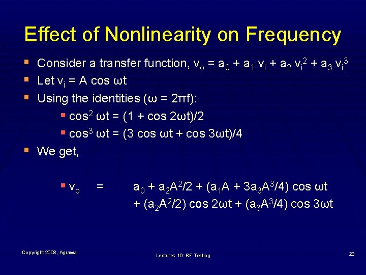
Effect of Nonlinearity on Frequency § § Consider a transfer function, vo = a 0 + a 1 vi + a 2 vi 2 + a 3 vi 3 Let vi = A cos ωt Using the identities (ω = 2πf): § cos 2 ωt = (1 + cos 2ωt)/2 § cos 3 ωt = (3 cos ωt + cos 3ωt)/4 We get, § vo Copyright 2008, Agrawal = a 0 + a 2 A 2/2 + (a 1 A + 3 a 3 A 3/4) cos ωt + (a 2 A 2/2) cos 2ωt + (a 3 A 3/4) cos 3ωt Lectures 16: RF Testing 23

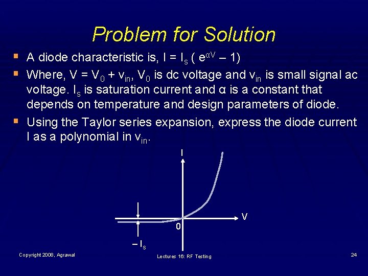
Problem for Solution § A diode characteristic is, I = Is ( eαV – 1) § Where, V = V 0 + vin, V 0 is dc voltage and vin is small signal ac § voltage. Is is saturation current and α is a constant that depends on temperature and design parameters of diode. Using the Taylor series expansion, express the diode current I as a polynomial in vin. I 0 V – Is Copyright 2008, Agrawal Lectures 16: RF Testing 24

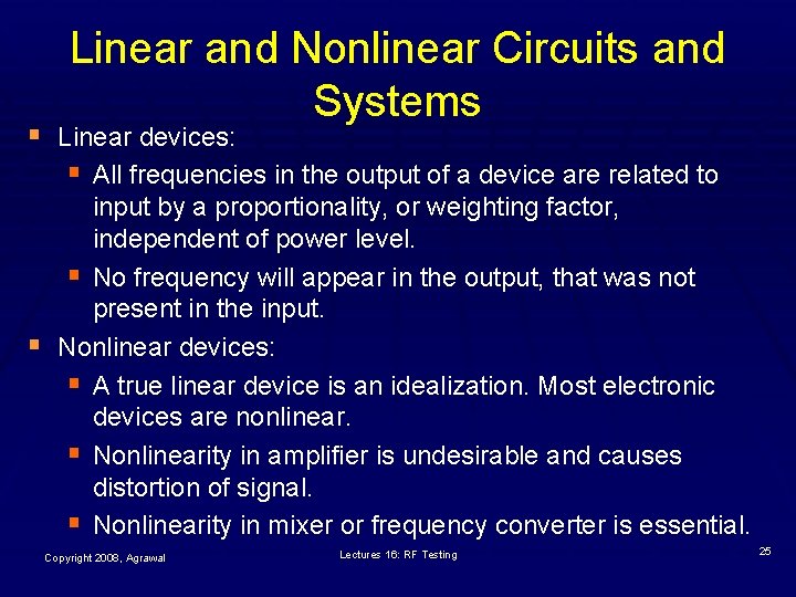
Linear and Nonlinear Circuits and Systems § Linear devices: § All frequencies in the output of a device are related to § input by a proportionality, or weighting factor, independent of power level. § No frequency will appear in the output, that was not present in the input. Nonlinear devices: § A true linear device is an idealization. Most electronic devices are nonlinear. § Nonlinearity in amplifier is undesirable and causes distortion of signal. § Nonlinearity in mixer or frequency converter is essential. Copyright 2008, Agrawal Lectures 16: RF Testing 25

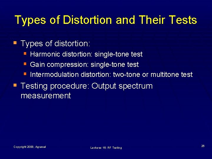
Types of Distortion and Their Tests § Types of distortion: § Harmonic distortion: single-tone test § Gain compression: single-tone test § Intermodulation distortion: two-tone or multitone test § Testing procedure: Output spectrum measurement Copyright 2008, Agrawal Lectures 16: RF Testing 26

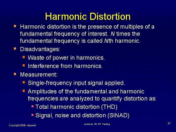
Harmonic Distortion § Harmonic distortion is the presence of multiples of a § § fundamental frequency of interest. N times the fundamental frequency is called Nth harmonic. Disadvantages: § Waste of power in harmonics. § Interference from harmonics. Measurement: § Single-frequency input signal applied. § Amplitudes of the fundamental and harmonic frequencies are analyzed to quantify distortion as: § Total harmonic distortion (THD) § Signal, noise and distortion (SINAD) Copyright 2008, Agrawal Lectures 16: RF Testing 27

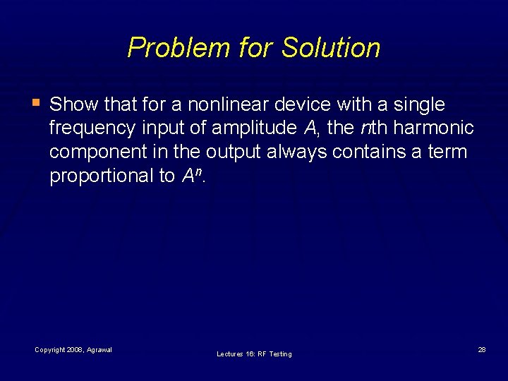
Problem for Solution § Show that for a nonlinear device with a single frequency input of amplitude A, the nth harmonic component in the output always contains a term proportional to An. Copyright 2008, Agrawal Lectures 16: RF Testing 28