VLSI Testing Lecture 17 RF Testing II Dr
![Other Noise Types § Shot noise [Schottky, 1928]: Broadband noise due to random § Other Noise Types § Shot noise [Schottky, 1928]: Broadband noise due to random §](https://slidetodoc.com/presentation_image/5178218b488f60e141d6d00ebca6f0c8/image-27.jpg)
![Phase Noise Analysis [V + δ(t)] sin [ωt + φ(t)] = [V + δ(t)] Phase Noise Analysis [V + δ(t)] sin [ωt + φ(t)] = [V + δ(t)]](https://slidetodoc.com/presentation_image/5178218b488f60e141d6d00ebca6f0c8/image-40.jpg)
- Slides: 45

VLSI Testing Lecture 17: RF Testing II Dr. Vishwani D. Agrawal James J. Danaher Professor of Electrical and Computer Engineering Auburn University, Alabama 36849, USA vagrawal@eng. auburn. edu http: //www. eng. auburn. edu/~vagrawal IIT Delhi, Aug 27, 2013, 2: 30 -4: 30 PM Copyright 2008, Agrawal Lectures 17: RF Testing II 1

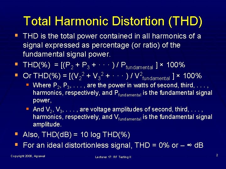
Total Harmonic Distortion (THD) § THD is the total power contained in all harmonics of a § § signal expressed as percentage (or ratio) of the fundamental signal power. THD(%) = [(P 2 + P 3 + · · · ) / Pfundamental ] × 100% Or THD(%) = [(V 22 + V 32 + · · · ) / V 2 fundamental ] × 100% § Where P 2, P 3, . . . , are the power in watts of second, third, . . . , § harmonics, respectively, and Pfundamental is the fundamental signal power, And V 2, V 3, . . . , are voltage amplitudes of second, third, . . . , harmonics, respectively, and Vfundamental is the fundamental signal amplitude. § Also, THD(d. B) = 10 log THD(%) § For an ideal distortionless signal, THD = 0% or – ∞ d. B Copyright 2008, Agrawal Lectures 17: RF Testing II 2

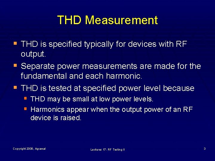
THD Measurement § THD is specified typically for devices with RF § § output. Separate power measurements are made for the fundamental and each harmonic. THD is tested at specified power level because § THD may be small at low power levels. § Harmonics appear when the output power of an RF device is raised. Copyright 2008, Agrawal Lectures 17: RF Testing II 3

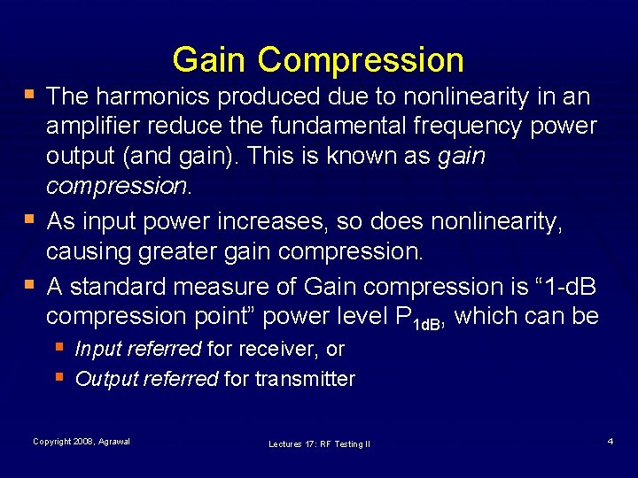
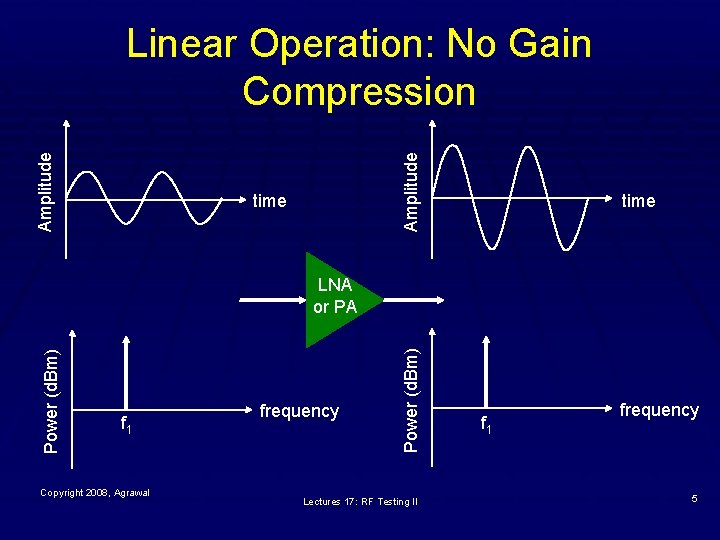
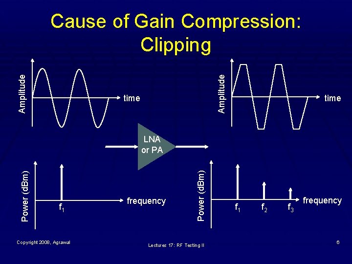
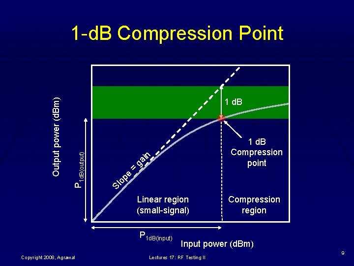
Gain Compression § The harmonics produced due to nonlinearity in an § § amplifier reduce the fundamental frequency power output (and gain). This is known as gain compression. As input power increases, so does nonlinearity, causing greater gain compression. A standard measure of Gain compression is “ 1 -d. B compression point” power level P 1 d. B, which can be § Input referred for receiver, or § Output referred for transmitter Copyright 2008, Agrawal Lectures 17: RF Testing II 4

Amplitude Linear Operation: No Gain Compression time f 1 Copyright 2008, Agrawal frequency Power (d. Bm) LNA or PA Lectures 17: RF Testing II f 1 frequency 5

Amplitude Cause of Gain Compression: Clipping time f 1 Copyright 2008, Agrawal frequency Power (d. Bm) LNA or PA Lectures 17: RF Testing II f 1 f 2 f 3 frequency 6

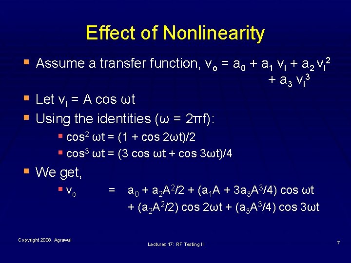
Effect of Nonlinearity § Assume a transfer function, vo = a 0 + a 1 vi + a 2 vi 2 § Let vi = A cos ωt § Using the identities (ω = 2πf): § + a 3 v i 3 § cos 2 ωt = (1 + cos 2ωt)/2 § cos 3 ωt = (3 cos ωt + cos 3ωt)/4 We get, § vo = a 0 + a 2 A 2/2 + (a 1 A + 3 a 3 A 3/4) cos ωt + (a 2 A 2/2) cos 2ωt + (a 3 A 3/4) cos 3ωt Copyright 2008, Agrawal Lectures 17: RF Testing II 7

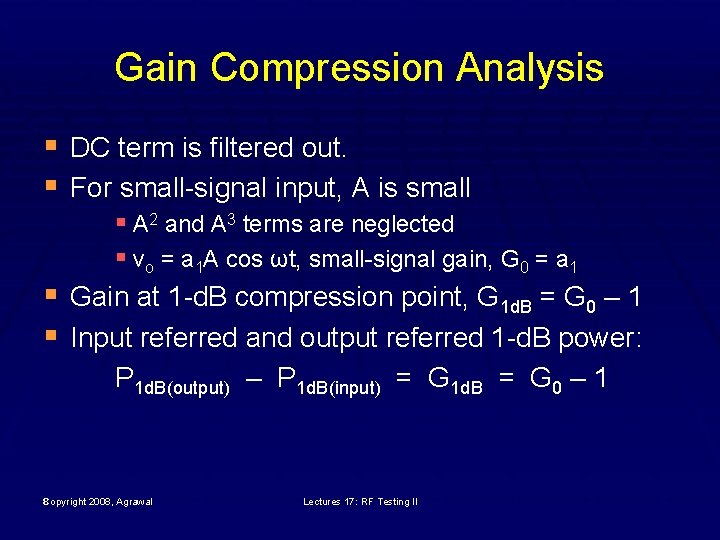
Gain Compression Analysis § DC term is filtered out. § For small-signal input, A is small § § § A 2 and A 3 terms are neglected § vo = a 1 A cos ωt, small-signal gain, G 0 = a 1 Gain at 1 -d. B compression point, G 1 d. B = G 0 – 1 Input referred and output referred 1 -d. B power: P 1 d. B(output) – P 1 d. B(input) = G 1 d. B = G 0 – 1 Copyright 2008, Agrawal 8 Lectures 17: RF Testing II

1 d. B op e = ga i n 1 d. B Compression point Sl P 1 d. B(output) Output power (d. Bm) 1 -d. B Compression Point Linear region (small-signal) P 1 d. B(input) Copyright 2008, Agrawal Compression region Input power (d. Bm) Lectures 17: RF Testing II 9

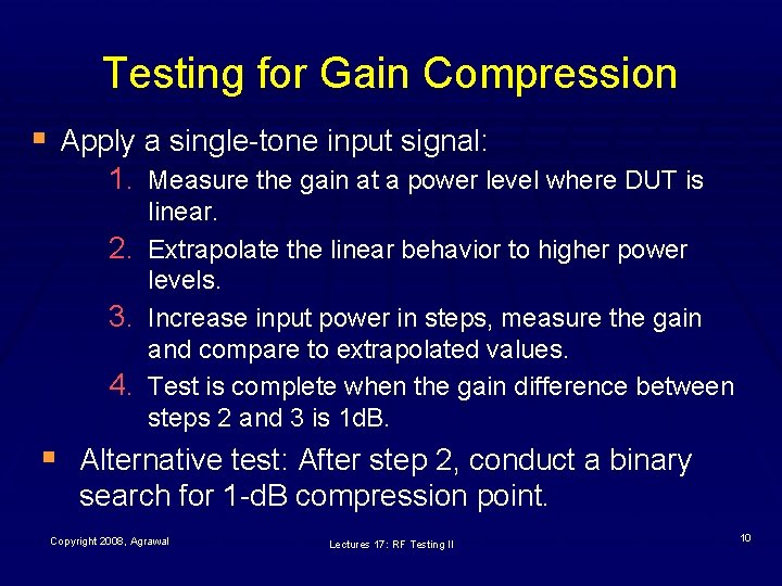
Testing for Gain Compression § Apply a single-tone input signal: 1. Measure the gain at a power level where DUT is linear. 2. Extrapolate the linear behavior to higher power levels. 3. Increase input power in steps, measure the gain and compare to extrapolated values. 4. Test is complete when the gain difference between steps 2 and 3 is 1 d. B. § Alternative test: After step 2, conduct a binary search for 1 -d. B compression point. Copyright 2008, Agrawal Lectures 17: RF Testing II 10

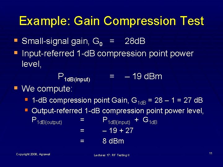
Example: Gain Compression Test § Small-signal gain, G 0 = 28 d. B § Input-referred 1 -d. B compression point power level, § P 1 d. B(input) = – 19 d. Bm We compute: § 1 -d. B compression point Gain, G 1 d. B = 28 – 1 = 27 d. B § Output-referred 1 -d. B compression point power level, P 1 d. B(output) Copyright 2008, Agrawal = = = P 1 d. B(input) + G 1 d. B – 19 + 27 8 d. Bm Lectures 17: RF Testing II 11

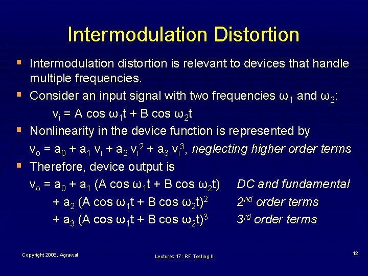
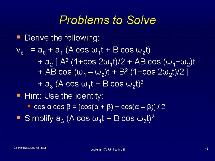
Intermodulation Distortion § Intermodulation distortion is relevant to devices that handle § § § multiple frequencies. Consider an input signal with two frequencies ω1 and ω2: vi = A cos ω1 t + B cos ω2 t Nonlinearity in the device function is represented by vo = a 0 + a 1 vi + a 2 vi 2 + a 3 vi 3, neglecting higher order terms Therefore, device output is vo = a 0 + a 1 (A cos ω1 t + B cos ω2 t) DC and fundamental + a 2 (A cos ω1 t + B cos ω2 t)2 2 nd order terms + a 3 (A cos ω1 t + B cos ω2 t)3 3 rd order terms Copyright 2008, Agrawal Lectures 17: RF Testing II 12

Problems to Solve § Derive the following: vo = a 0 + a 1 (A cos ω1 t + B cos ω2 t) + a 2 [ A 2 (1+cos 2ω1 t)/2 + AB cos (ω1+ω2)t + AB cos (ω1 – ω2)t + B 2 (1+cos 2ω2 t)/2 ] + a 3 (A cos ω1 t + B cos ω2 t)3 § Hint: Use the identity: § cos α cos β = [cos(α + β) + cos(α – β)] / 2 § Simplify a 3 (A cos ω1 t + B cos ω2 t)3 Copyright 2008, Agrawal Lectures 17: RF Testing II 13

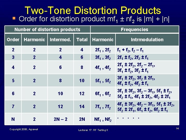
Two-Tone Distortion Products § Order for distortion product mf 1 ± nf 2 is |m| + |n| Nunber of distortion products Order Harmonic Frequencies Intermod. Total Harmonic Intrmodulation 2 2 2 4 2 f 1 , 2 f 2 f 1 + f 2 , f 2 – f 1 3 2 4 6 3 f 1 , 3 f 2 2 f 1 ± f 2, 2 f 2 ± f 1 4 2 6 8 4 f 1 , 4 f 2 2 f 1 ± 2 f 2, 2 f 2 – 2 f 1, 3 f 1 ± f 2, 3 f 2 ± f 1 5 2 8 10 5 f 1 , 5 f 2 3 f 1 ± 2 f 2, 3 f 2 ± 2 f 1, 4 f 1 ± f 2, 4 f 2 ± f 1 6 2 10 12 6 f 1 , 6 f 2 3 f 1 ± 3 f 2, 3 f 2 – 3 f 1, 5 f 1 ± f 2, 5 f 2 ± f 1, 4 f 1 ± 2 f 2, 4 f 2 ± 2 f 1 7 2 12 14 7 f 1 , 7 f 2 4 f 1 ± 3 f 2, 4 f 2 – 3 f 1, 5 f 1 ± 2 f 2, 5 f 2 ± 2 f 1, 6 f 1 ± f 2, 6 f 2 ± f 1 N 2 2 N – 2 2 N Nf 1 , Nf 2 Copyright 2008, Agrawal Lectures 17: RF Testing II . . . 14

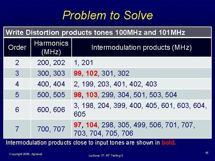
Problem to Solve Write Distortion products tones 100 MHz and 101 MHz Harmonics Order Intermodulation products (MHz) 2 200, 202 1, 201 3 300, 303 99, 102, 301, 302 4 400, 404 2, 199, 203, 401, 402, 403 5 500, 505 98, 103, 299, 304, 501, 503, 504 3, 198, 204, 399, 400, 405, 601, 603, 604, 6 600, 606 605 97, 104, 298, 305, 499, 506, 701, 707, 7 700, 707 703, 704, 705, 706 Intermodulation products close to input tones are shown in bold. Copyright 2008, Agrawal Lectures 17: RF Testing II 15

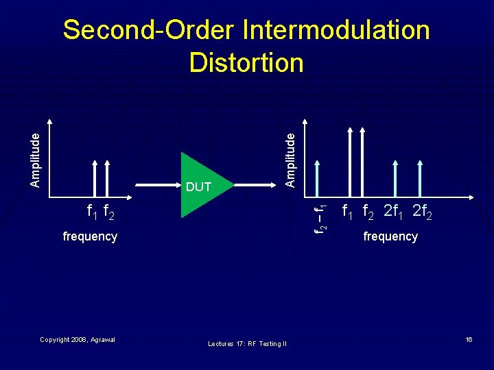
DUT Amplitude Second-Order Intermodulation Distortion f 2 – f 1 f 2 frequency Copyright 2008, Agrawal Lectures 17: RF Testing II f 1 f 2 2 f 1 2 f 2 frequency 16

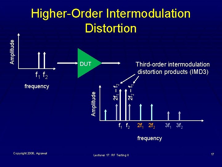
Amplitude Higher-Order Intermodulation Distortion DUT Third-order intermodulation distortion products (IMD 3) 2 f 2 – f 1 Amplitude frequency 2 f 1 – f 2 f 1 f 2 2 f 1 2 f 2 3 f 1 3 f 2 frequency Copyright 2008, Agrawal Lectures 17: RF Testing II 17

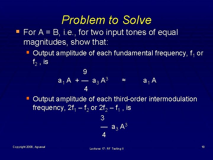
Problem to Solve § For A = B, i. e. , for two input tones of equal magnitudes, show that: § Output amplitude of each fundamental frequency, f 1 or f 2 , is § 9 a 1 A + — a 3 A 3 ≈ a 1 A 4 Output amplitude of each third-order intermodulation frequency, 2 f 1 – f 2 or 2 f 2 – f 1 , is 3 — a 3 A 3 4 Copyright 2008, Agrawal Lectures 17: RF Testing II 18

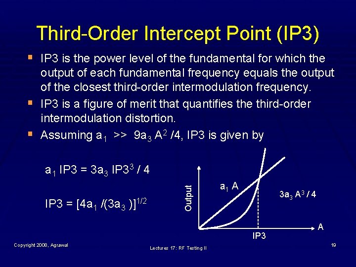
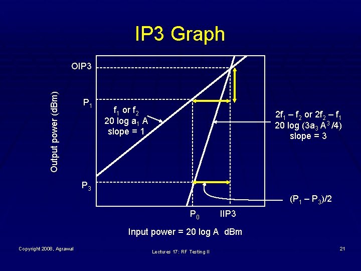
Third-Order Intercept Point (IP 3) § IP 3 is the power level of the fundamental for which the § § output of each fundamental frequency equals the output of the closest third-order intermodulation frequency. IP 3 is a figure of merit that quantifies the third-order intermodulation distortion. Assuming a 1 >> 9 a 3 A 2 /4, IP 3 is given by IP 3 = [4 a 1 /(3 a 3 )]1/2 Output a 1 IP 3 = 3 a 3 IP 33 / 4 a 1 A 3 a 3 A 3 / 4 IP 3 Copyright 2008, Agrawal Lectures 17: RF Testing II A 19

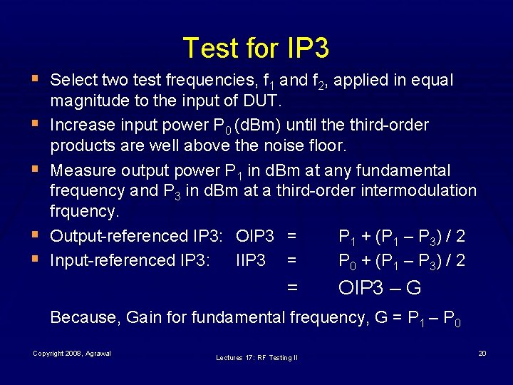
Test for IP 3 § Select two test frequencies, f 1 and f 2, applied in equal § § magnitude to the input of DUT. Increase input power P 0 (d. Bm) until the third-order products are well above the noise floor. Measure output power P 1 in d. Bm at any fundamental frequency and P 3 in d. Bm at a third-order intermodulation frquency. Output-referenced IP 3: OIP 3 = P 1 + (P 1 – P 3) / 2 Input-referenced IP 3: IIP 3 = P 0 + (P 1 – P 3) / 2 = OIP 3 – G Because, Gain for fundamental frequency, G = P 1 – P 0 Copyright 2008, Agrawal Lectures 17: RF Testing II 20

IP 3 Graph Output power (d. Bm) OIP 3 P 1 f 1 or f 2 20 log a 1 A slope = 1 2 f 1 – f 2 or 2 f 2 – f 1 20 log (3 a 3 A 3 /4) slope = 3 P 3 (P 1 – P 3)/2 P 0 IIP 3 Input power = 20 log A d. Bm Copyright 2008, Agrawal Lectures 17: RF Testing II 21

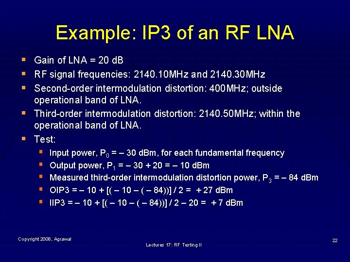
Example: IP 3 of an RF LNA § § § Gain of LNA = 20 d. B RF signal frequencies: 2140. 10 MHz and 2140. 30 MHz Second-order intermodulation distortion: 400 MHz; outside operational band of LNA. Third-order intermodulation distortion: 2140. 50 MHz; within the operational band of LNA. Test: § § § Input power, P 0 = – 30 d. Bm, for each fundamental frequency Output power, P 1 = – 30 + 20 = – 10 d. Bm Measured third-order intermodulation distortion power, P 3 = – 84 d. Bm OIP 3 = – 10 + [( – 10 – ( – 84))] / 2 = + 27 d. Bm IIP 3 = – 10 + [( – 10 – ( – 84))] / 2 – 20 = + 7 d. Bm Copyright 2008, Agrawal Lectures 17: RF Testing II 22

What is Noise? § Noise in an RF system is unwanted random fluctuations in a desired § § § signal. Noise is a natural phenomenon and is always present in the environment. Effects of noise: § Interferes with detection of signal (hides the signal). § Causes errors in information transmission by changing signal. § Sometimes noise might imitate a signal falsely. All communications system design and operation must account for noise. Copyright 2008, Agrawal Lectures 17: RF Testing II 23

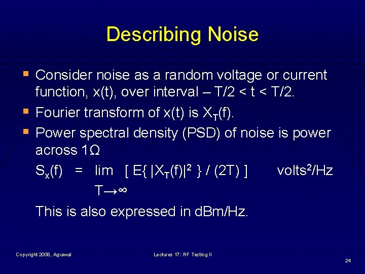
Describing Noise § Consider noise as a random voltage or current § § function, x(t), over interval – T/2 < t < T/2. Fourier transform of x(t) is XT(f). Power spectral density (PSD) of noise is power across 1Ω Sx(f) = lim [ E{ |XT(f)|2 } / (2 T) ] volts 2/Hz T→∞ This is also expressed in d. Bm/Hz. Copyright 2008, Agrawal Lectures 17: RF Testing II 24

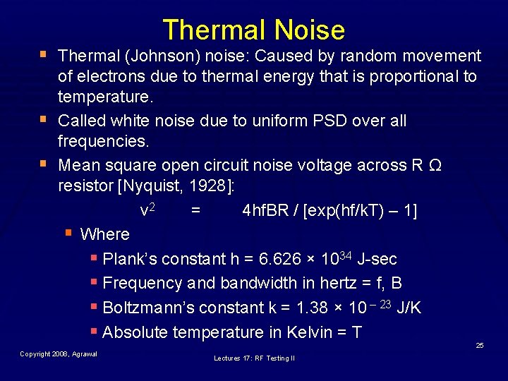
Thermal Noise § Thermal (Johnson) noise: Caused by random movement § § of electrons due to thermal energy that is proportional to temperature. Called white noise due to uniform PSD over all frequencies. Mean square open circuit noise voltage across R Ω resistor [Nyquist, 1928]: v 2 = 4 hf. BR / [exp(hf/k. T) – 1] § Where § Plank’s constant h = 6. 626 × 1034 J-sec § Frequency and bandwidth in hertz = f, B § Boltzmann’s constant k = 1. 38 × 10 – 23 J/K § Absolute temperature in Kelvin = T 25 Copyright 2008, Agrawal Lectures 17: RF Testing II

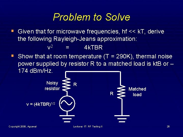
Problem to Solve § Given that for microwave frequencies, hf << k. T, derive § the following Rayleigh-Jeans approximation: v 2 = 4 k. TBR Show that at room temperature (T = 290 K), thermal noise power supplied by resistor R to a matched load is kt. B or – 174 d. Bm/Hz. Noisy resistor R R Matched load v = (4 k. TBR)1/2 Copyright 2008, Agrawal Lectures 17: RF Testing II 26
![Other Noise Types Shot noise Schottky 1928 Broadband noise due to random Other Noise Types § Shot noise [Schottky, 1928]: Broadband noise due to random §](https://slidetodoc.com/presentation_image/5178218b488f60e141d6d00ebca6f0c8/image-27.jpg)
Other Noise Types § Shot noise [Schottky, 1928]: Broadband noise due to random § § behavior of charge carriers in semiconductor devices. Flicker (1/f) noise: Low-frequency noise in semiconductor devices, perhaps due to material defects; power spectrum falls off as 1/f. Can be significant at audio frequencies. Quantization noise: Caused by conversion of continuous valued analog signal to discrete-valued digital signal; minimized by using more digital bits. Quantum noise: Broadband noise caused by the quantized nature of charge carriers; significant at very low temperatures (~0 K) or very high bandwidth ( > 1015 Hz). Plasma noise: Caused by random motion of charges in ionized medium, possibly resulting from sparking in electrical contacts; generally, not a concern. Copyright 2008, Agrawal 27 Lectures 17: RF Testing II

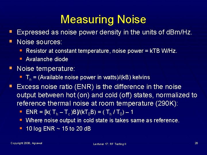
Measuring Noise § Expressed as noise power density in the units of d. Bm/Hz. § Noise sources: § Resistor at constant temperature, noise power = k. TB W/Hz. § Avalanche diode § Noise temperature: § Tn = (Available noise power in watts)/(k. B) kelvins § Excess noise ratio (ENR) is the difference in the noise output between hot (on) and cold (off) states, normalized to reference thermal noise at room temperature (290 K): § ENR = [k( Th – Tc )B]/(k. T 0 B) = ( Th / T 0) – 1 § Where noise output in cold state is takes same as reference. § 10 log ENR ~ 15 to 20 d. B Copyright 2008, Agrawal Lectures 17: RF Testing II 28

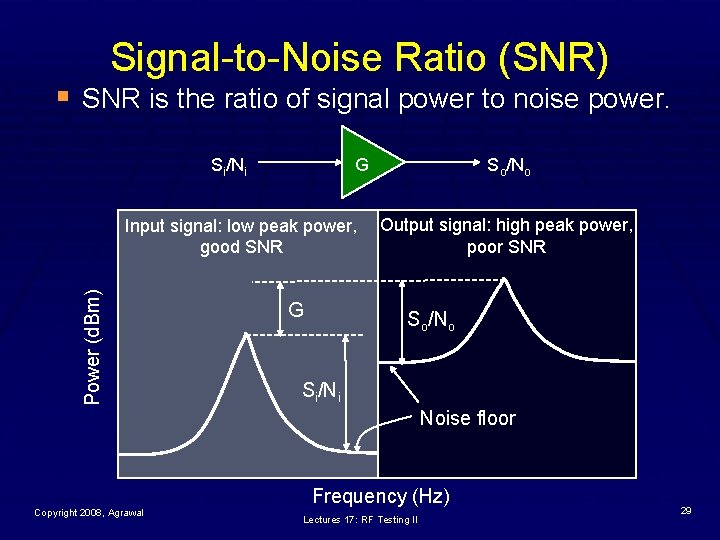
Signal-to-Noise Ratio (SNR) § SNR is the ratio of signal power to noise power. Si/Ni G Power (d. Bm) Input signal: low peak power, good SNR G So/No Output signal: high peak power, poor SNR So/No Si/Ni Noise floor Copyright 2008, Agrawal Frequency (Hz) Lectures 17: RF Testing II 29

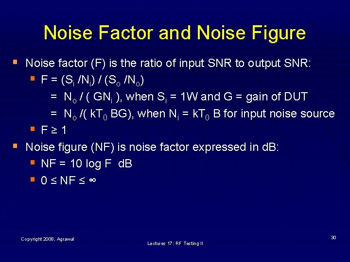
Noise Factor and Noise Figure § Noise factor (F) is the ratio of input SNR to output SNR: § F = (Si /Ni) / (So /No) § = No / ( GNi ), when Si = 1 W and G = gain of DUT = No /( k. T 0 BG), when Ni = k. T 0 B for input noise source § F≥ 1 Noise figure (NF) is noise factor expressed in d. B: § NF = 10 log F d. B § 0 ≤ NF ≤ ∞ Copyright 2008, Agrawal Lectures 17: RF Testing II 30

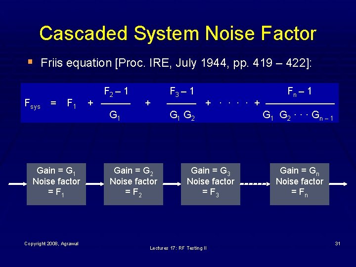
Cascaded System Noise Factor § Friis equation [Proc. IRE, July 1944, pp. 419 – 422]: Fsys = F 1 Gain = G 1 Noise factor = F 1 Copyright 2008, Agrawal F 2 – 1 + ——— G 1 + Gain = G 2 Noise factor = F 2 F 3 – 1 Fn – 1 ——— + · · + ——————— G 1 G 2 · · · G n – 1 Gain = G 3 Noise factor = F 3 Lectures 17: RF Testing II Gain = Gn Noise factor = Fn 31

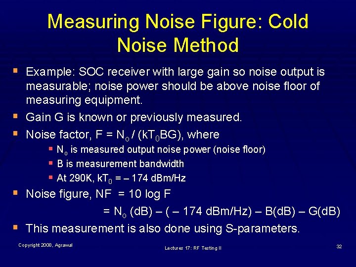
Measuring Noise Figure: Cold Noise Method § Example: SOC receiver with large gain so noise output is § § measurable; noise power should be above noise floor of measuring equipment. Gain G is known or previously measured. Noise factor, F = No / (k. T 0 BG), where § No is measured output noise power (noise floor) § B is measurement bandwidth § At 290 K, k. T 0 = – 174 d. Bm/Hz Noise figure, NF = 10 log F = No (d. B) – ( – 174 d. Bm/Hz) – B(d. B) – G(d. B) This measurement is also done using S-parameters. Copyright 2008, Agrawal Lectures 17: RF Testing II 32

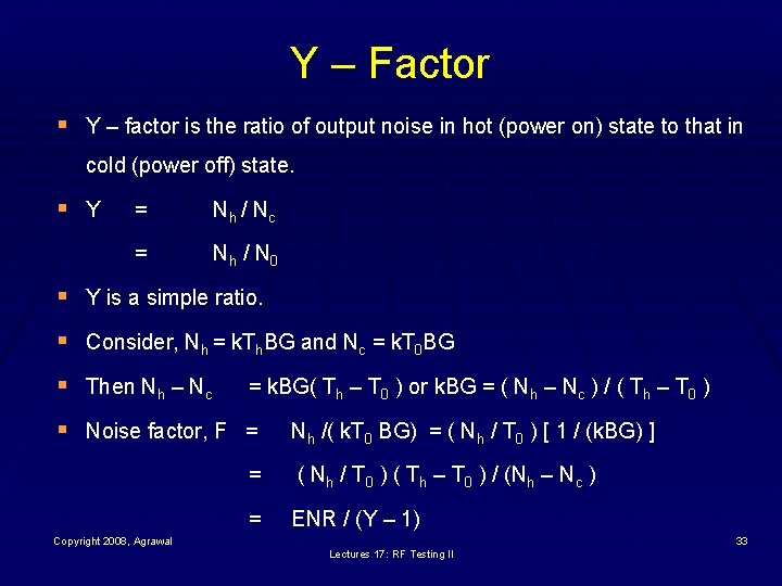
Y – Factor § Y – factor is the ratio of output noise in hot (power on) state to that in cold (power off) state. § Y = Nh / N c = Nh / N 0 § Y is a simple ratio. § Consider, Nh = k. Th. BG and Nc = k. T 0 BG § Then Nh – Nc = k. BG( Th – T 0 ) or k. BG = ( Nh – Nc ) / ( Th – T 0 ) § Noise factor, F = Nh /( k. T 0 BG) = ( Nh / T 0 ) [ 1 / (k. BG) ] = ( Nh / T 0 ) ( Th – T 0 ) / (Nh – Nc ) = ENR / (Y – 1) Copyright 2008, Agrawal 33 Lectures 17: RF Testing II

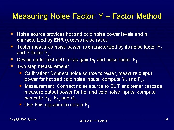
Measuring Noise Factor: Y – Factor Method § Noise source provides hot and cold noise power levels and is § § § characterized by ENR (excess noise ratio). Tester measures noise power, is characterized by its noise factor F 2 and Y-factor Y 2. Device under test (DUT) has gain G 1 and noise factor F 1. Two-step measurement: § Calibration: Connect noise source to tester, measure output power for hot and cold noise inputs, compute Y 2 and F 2. § Measurement: Connect noise source to DUT and tester cascade, measure output power for hot and cold noise inputs, compute Y 12, F 12 and G 1. § Use Friis equation to obtain F 1. Copyright 2008, Agrawal Lectures 17: RF Testing II 34

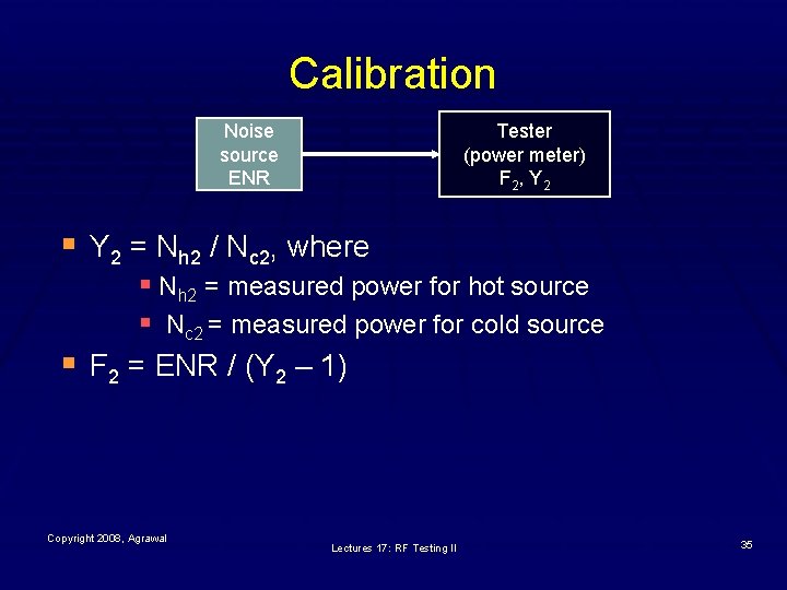
Calibration Noise source ENR Tester (power meter) F 2 , Y 2 § Y 2 = Nh 2 / Nc 2, where § § Nh 2 = measured power for hot source § Nc 2 = measured power for cold source F 2 = ENR / (Y 2 – 1) Copyright 2008, Agrawal Lectures 17: RF Testing II 35

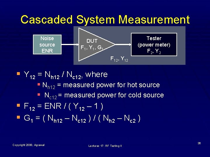
Cascaded System Measurement Noise source ENR Tester (power meter) F 2 , Y 2 DUT F 1 , Y 1 , G 1 F 12, Y 12 § Y 12 = Nh 12 / Nc 12, where § § § Nh 12 = measured power for hot source § Nc 12 = measured power for cold source F 12 = ENR / ( Y 12 – 1 ) G 1 = ( Nh 12 – Nc 12 ) / ( Nh 2 – Nc 2 ) Copyright 2008, Agrawal Lectures 17: RF Testing II 36

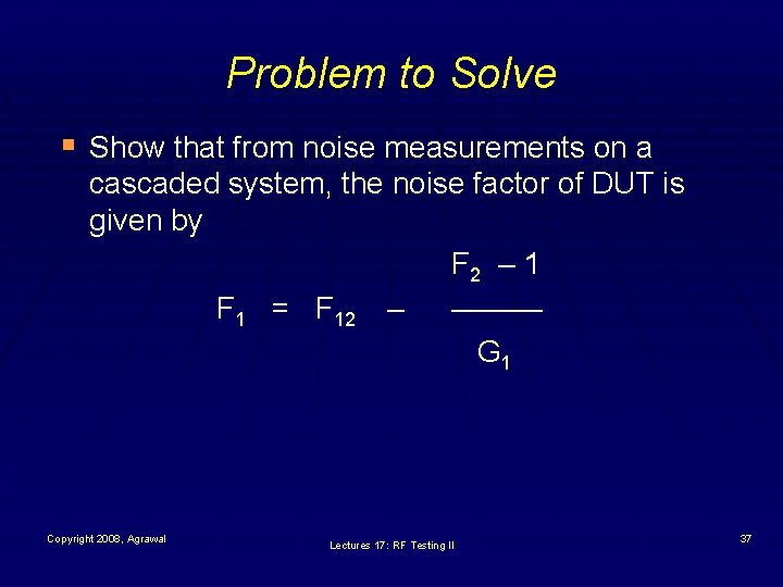
Problem to Solve § Show that from noise measurements on a cascaded system, the noise factor of DUT is given by F 2 – 1 F 1 = F 12 – ——— G 1 Copyright 2008, Agrawal Lectures 17: RF Testing II 37

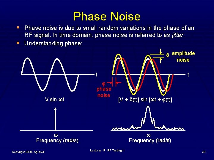
Phase Noise § Phase noise is due to small random variations in the phase of an § RF signal. In time domain, phase noise is referred to as jitter. Understanding phase: δ amplitude noise t V sin ωt φ phase noise t [V + δ(t)] sin [ωt + φ(t)] ω Frequency (rad/s) Copyright 2008, Agrawal ω Frequency (rad/s) Lectures 17: RF Testing II 38

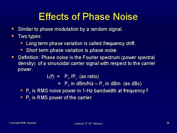
Effects of Phase Noise § Similar to phase modulation by a random signal. § Two types: § Long term phase variation is called frequency drift. § Short term phase variation is phase noise. § Definition: Phase noise is the Fourier spectrum (power spectral density) of a sinusoidal carrier signal with respect to the carrier power. L(f) = Pn /Pc (as ratio) = Pn in d. Bm/Hz – Pc in d. Bm (as d. Bc) § Pn is RMS noise power in 1 -Hz bandwidth at frequency f § Pc is RMS power of the carrier Copyright 2008, Agrawal Lectures 17: RF Testing II 39
![Phase Noise Analysis V δt sin ωt φt V δt Phase Noise Analysis [V + δ(t)] sin [ωt + φ(t)] = [V + δ(t)]](https://slidetodoc.com/presentation_image/5178218b488f60e141d6d00ebca6f0c8/image-40.jpg)
Phase Noise Analysis [V + δ(t)] sin [ωt + φ(t)] = [V + δ(t)] [sin ωt cos φ(t) + cos ωt sin φ(t)] ≈ [V + δ(t)] sin ωt + [V + δ(t)] φ(t) cos ωt In-phase carrier frequency with amplitude noise White noise δ(t) corresponds to noise floor Quadrature-phase carrier frequency with amplitude and phase noise Short-term phase noise corresponds to phase noise spectrum Phase spectrum, L(f) = Sφ(f)/2 Where Sφ(f) is power spectrum of φ(t) Copyright 2008, Agrawal Lectures 17: RF Testing II 40

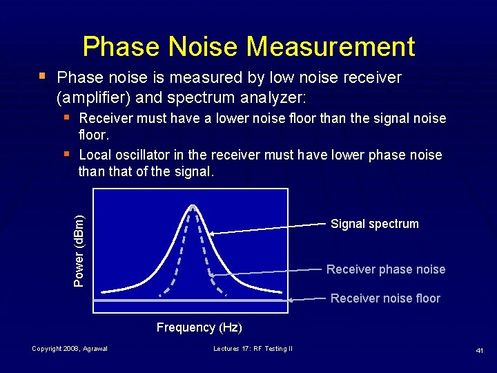
Phase Noise Measurement § Phase noise is measured by low noise receiver (amplifier) and spectrum analyzer: § Receiver must have a lower noise floor than the signal noise Power (d. Bm) § floor. Local oscillator in the receiver must have lower phase noise than that of the signal. Signal spectrum Receiver phase noise Receiver noise floor Frequency (Hz) Copyright 2008, Agrawal Lectures 17: RF Testing II 41

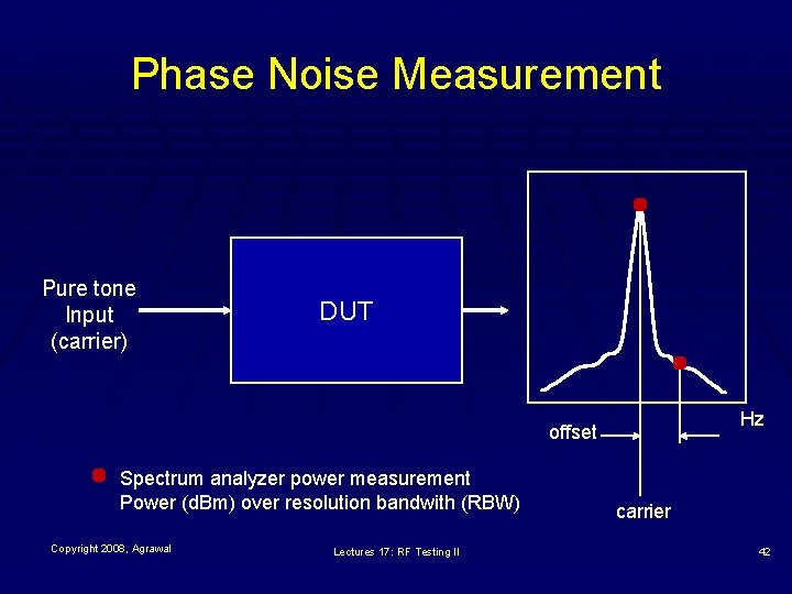
Phase Noise Measurement Pure tone Input (carrier) DUT Hz offset Spectrum analyzer power measurement Power (d. Bm) over resolution bandwith (RBW) Copyright 2008, Agrawal Lectures 17: RF Testing II carrier 42

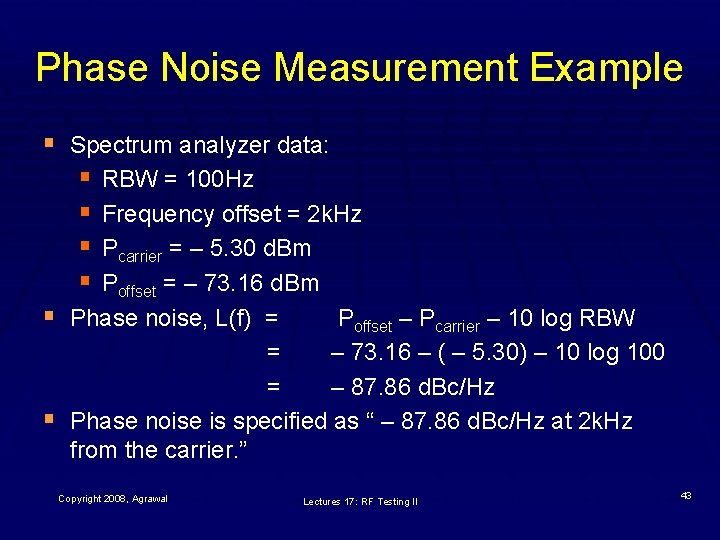
Phase Noise Measurement Example § Spectrum analyzer data: § RBW = 100 Hz § Frequency offset = 2 k. Hz § Pcarrier = – 5. 30 d. Bm § Poffset = – 73. 16 d. Bm § Phase noise, L(f) = Poffset – Pcarrier – 10 log RBW § = – 73. 16 – ( – 5. 30) – 10 log 100 = – 87. 86 d. Bc/Hz Phase noise is specified as “ – 87. 86 d. Bc/Hz at 2 k. Hz from the carrier. ” Copyright 2008, Agrawal Lectures 17: RF Testing II 43

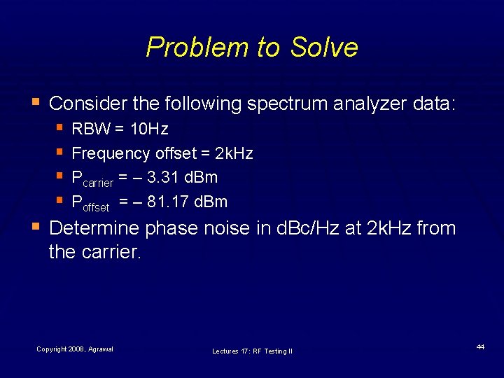
Problem to Solve § Consider the following spectrum analyzer data: § RBW = 10 Hz § Frequency offset = 2 k. Hz § Pcarrier = – 3. 31 d. Bm § Poffset = – 81. 17 d. Bm § Determine phase noise in d. Bc/Hz at 2 k. Hz from the carrier. Copyright 2008, Agrawal Lectures 17: RF Testing II 44

References, Again 1. S. Bhattacharya and A. Chatterjee, "RF Testing, " Chapter 16, pages 2. 3. 4. 5. 6. 745 -789, in System on Chip Test Architectures, edited by L. -T. Wang, C. E. Stroud and N. A. Touba, Amsterdam: Morgan-Kaufman, 2008. M. L. Bushnell and V. D. Agrawal, Essentials of Electronic Testing for Digital, Memory & Mixed-Signal VLSI Circuits, Boston: Springer, 2000. J. Kelly and M. Engelhardt, Advanced Production Testing of RF, So. C, and Si. P Devices, Boston: Artech House, 2007. B. Razavi, RF Microelectronics, Upper Saddle River, New Jersey: Prentice Hall PTR, 1998. J. Rogers, C. Plett and F. Dai, Integrated Circuit Design for High-Speed Frequency Synthesis, Boston: Artech House, 2006. K. B. Schaub and J. Kelly, Production Testing of RF and System-on-a. Chip Devices for Wireless Communications, Boston: Artech House, 2004. Copyright 2008, Agrawal Lectures 17: RF Testing II 45