The ITRS MPU and SOC System Drivers Calibration
The ITRS MPU and SOC System Drivers: Calibration and Implications for Design-Based Equivalent Scaling in the Roadmap Wei-Ting Jonas Chan 1 Andrew B. Kahng 1, 2 Siddhartha Nath 2 Ichiro Yamamoto 3 1 ECE and 2 CSE Departments, UC San Diego, USA 3 Rohm Co. Ltd. , Japan ICCD-2014, 141020 1
Outline • Overview of ITRS Design and System Drivers Roadmaps • Architectural and Area Models of MPU and SOC • Design Capacity Gap and Design Equivalent Scaling • Power Modeling and Power Management Gap • Conclusions ICCD-2014, 141020 2

The ITWGs • International Technology Working Groups (ITWGs) forecast technology requirements, potential solutions 15 -year horizon • Emerging Devices, Emerging Materials: +10 more years outlook System Drivers Design Process Integ, Devices & Structures Front End Processes Emerging Research Devices Emerging Research Materials Lithography Interconnect Factory Integration Assembly & Packaging Test and Test Equipment Metrology Yield Enhancement Modeling & Simulation Environment, Safety & Health RF/AMS Tech for Wireless Comm Each regional working group = industry + government + suppliers + consortia + academia ICCD-2014, 141020 3
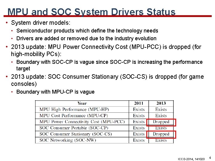
MPU and SOC System Drivers Status • System driver models: • Semiconductor products which define the technology needs • Drivers are added or removed due to the industry evolution • 2013 update: MPU Power Connectivity Cost (MPU-PCC) is dropped (for high-mobility PCs): • Boundary with SOC-CP is vague since SOC-CP is increasing the performance target • 2013 update: SOC Consumer Stationary (SOC-CS) is dropped (for game consoles) • Boundary with MPU-CP is vague ICCD-2014, 141020 4

Outline • Overview of ITRS Design and System Drivers Chapters • Architectural and Area Models of MPU and SOC • Design Capacity Gap and Design Equivalent Scaling • Power Modeling and Power Management Gap • Conclusions ICCD-2014, 141020 5

Heartbeat of the ITRS: Technology Nodes • Key metric of (density) progress: half-pitch (F) • Metal-1 (M 1) half-pitch scales by 0. 7 x • 0. 7 x 0. 7 = 0. 49 density doubles at each “technology node” Layer F Normalizations to PM 1 2009 2013 0. 50 M 1 Pitch (PM 1) 1. 00 M 2 Pitch (PM 2) 1. 25 1. 00 Contacted Poly Pitch (CPP) (Ppoly) 1. 50 Fin Pitch (Pfin) -- 0. 75 P/G Track Width -- 1. 50 Scaling in both X, Y dimensions ICCD-2014, 141020 6

Logic A-factor Model with Fin. FET (2013) • Logic A-factor models developed using NAND 2 layout (UNAND 2) area now use Fin. FET devices • New patterning limiter: Pfin • Assumption: Pfin = 0. 75 PM 1 3 Ppoly Contact WAS: NAND 2 A-factor = 175 in 2011 model IS: NAND 2 A-factor = 155 in 2013 model NWell Poly P/G Rail Mx Poly Contact Fin Metal VIAx MOL VIA 0 9 PM 2 Ulogic = 3 Ppoly 9 PM 2 = 162 F 2 calibrated 155 F 2 ICCD-2014, 141020 7
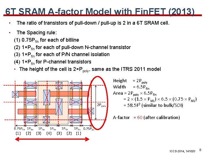
6 T SRAM A-factor Model with Fin. FET (2013) • • The ratio of transistors of pull-down / pull-up is 2 in a 6 T SRAM cell. The Spacing rule: (1) 0. 75 Pfin for each of bitline (2) 1×Pfin for each of pull-down N-channel transistor (3) 1×Pfin for each of P/N channel isolation (4) 1×Pfin for P-channel transistors • The height of the cell is 2×Ppoly, same as the ITRS 2011 model Height = 2 Ppoly Width = 6. 5 Pfin Area = 2 Ppoly × 6. 5 Pfin = 2 × (1. 5 × PM 1) × 6. 5 × (0. 75 × PM 1) = 58. 5 F 2 (similar to bulk/SOI) A-factor = 60 (after calibration) (1) (2) (3) (4) (3) (2) (1) ICCD-2014, 141020 8
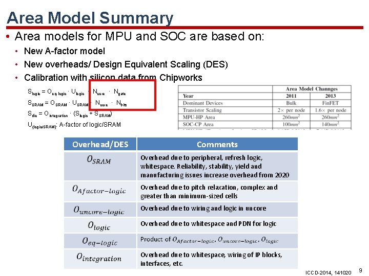
Area Model Summary • Area models for MPU and SOC are based on: • New A-factor model • New overheads/ Design Equivalent Scaling (DES) • Calibration with silicon data from Chipworks Slogic = Oeq-logic ∙ Ulogic ∙ Ncore ∙ Ngate SSRAM = OSRAM ∙ USRAM ∙ Ncore ∙ Nbits Sdie = Ointegration ∙ (Slogic + SSRAM) U{logic/SRAM}: A-factor of logic/SRAM Overhead/DES Comments Overhead due to peripheral, refresh logic, whitespace. Reliability, stability, yield and manufacturing issues increase overhead from 2020 Overhead due to pitch relaxation, complex and greater than minimum-sized cells Overhead due to wiring and logic in uncore Overhead due to whitespace and PDN for logic Overhead due to whitespace, wiring of IP blocks, interfaces, etc. ICCD-2014, 141020 9

MPU Model Revision Ologic core 1 • Calibrated Ointegration • + Previous overheads • OSRAM • Ologic core 2 Accelerators Memory Controller core 4 SRAM 2 SRAM 5 core 3 • New overheads • Ouncore-logic • OAfactor-logic Ouncore-logic SRAM 1 GPUs SRAM 3 OSRAM I/O interfaces SRAM 4 Key components to address different densities and overheads: • Logic • SRAM • Uncore (new in 2013 model) OAfactor-logic Ointegration ICCD-2014, 141020 10

SOC-CP Model Revision • Reference application of SOC-CP is changing • WAS: feature phones with basic applications (by processing engines, PE) • IS: smartphones with rich multimedia/gaming applications • GPU now key component in mobile AP • Design challenge of SOC-CP high diversity of functionalities IS: SOC-CP for smart phone Area: 140 mm 2 WAS: SOC-CP for mobile phone Area: 100 mm 2 Audio Bluetooth 2 D graphics Modem Audio Bluetooth Video Wifi Multi-modem ICCD-2014, 141020 11

SOC-CP Area Trend • WAS: PE / Memory dominate • IS: GPU dominates area (19% in 2013, 44% in 2028) 160. 00 140. 00 Area [mm^2] 120. 00 100. 00 80. 00 60. 00 40. 00 2013 2014 2015 2016 2017 2018 2019 2020 2021 2022 2023 2024 2025 2026 2027 2028 Year Main Memory [mm^2] MPU [mm^2] PE [mm^2] (NEW) GPU [mm^2] (NEW) IO [mm^2] (NEW) RF [mm^2] Interation Overhead Area [mm^2] ICCD-2014, 141020 12

SOC-CP Performance Challenge • Performance requirement is extrapolated from historical demands • Available processing performance improvement • Improved by faster devices • Improved by increasing #PE and GPUs • Significant gap after 2015 calls out for desperate demand for architecture and design methodology improvements {Processing performance} = {#main processors}×{main processor frequency}+ {#GPUs}×{GPU frequency} Performance gap ICCD-2014, 141020 13
Outline • Overview of ITRS Design and System Drivers Chapters • Architectural and Area Models of MPU and SOC • Design Capacity Gap and Design Equivalent Scaling • Power Modeling and Power Management Gap • Conclusions ICCD-2014, 141020 14
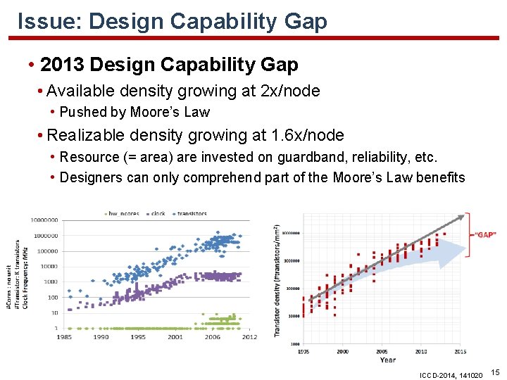
Issue: Design Capability Gap • 2013 Design Capability Gap • Available density growing at 2 x/node • Pushed by Moore’s Law • Realizable density growing at 1. 6 x/node • Resource (= area) are invested on guardband, reliability, etc. • Designers can only comprehend part of the Moore’s Law benefits ICCD-2014, 141020 15
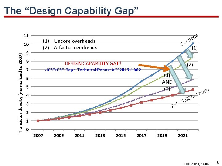
The “Design Capability Gap” 11 Transistor density (normalized to 2007) 10 9 o / n (1) Uncore overheads (2) A-factor overheads 8 2 x DESIGN CAPABILITY GAP! 7 de (1) (2) UCSD CSE Dept. Technical Report #CS 2013 -1002 (1) AND (2) 6 5 4 de no x / 87 1. 5 2/3 ~ 2 3 2 1 0 2007 2009 2011 2013 2015 2017 2019 2021 ICCD-2014, 141020 16
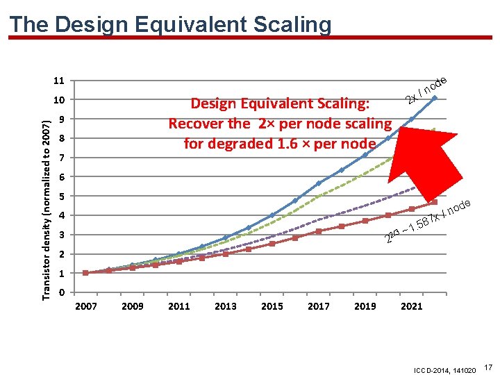
The Design Equivalent Scaling 11 Design Equivalent Scaling: Recover the 2× per node scaling for degraded 1. 6 × per node Transistor density (normalized to 2007) 10 9 8 7 o / n de 2 x 6 5 de 4 no x / 87 1. 5 2/3 ~ 2 3 2 1 0 2007 2009 2011 2013 2015 2017 2019 2021 ICCD-2014, 141020 17

Outline • Overview of ITRS Design and System Drivers Chapters • Architectural and Area Models of MPU and SOC • Design Capacity Gap and Design Equivalent Scaling • Power Modeling and Power Management Gap • Conclusions ICCD-2014, 141020 18
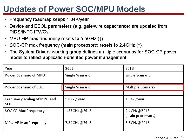
Updates of Power SOC/MPU Models • Frequency roadmap keeps 1. 04×/year • Device and BEOL parameters (e. g. gate/wire capacitance) are updated from PIDS/INTC ITWGs • MPU-HP max frequency resets to 5. 5 GHz (↓) • SOC-CP max frequency (main processors) resets to 2. 4 GHz (↑) • The System Drivers working group defines multiple scenarios for SOC-CP power model to reflect application-oriented power management Year 2011 2013 Power Scenario of MPU Single Scenario Power Scenario of SOC Single Scenario Multiple Scenario Frequency scaling of MPU and SOC 1. 04 x / year 1. 04 x /year SOC-CP Max Frequency 1. 37 GHz@2013 2. 4 GHz@2013 (main processors) MPU-HP Max Frequency 7. 34 GHz@2013 5. 5 GHz@2013 ICCD-2014, 141020 19
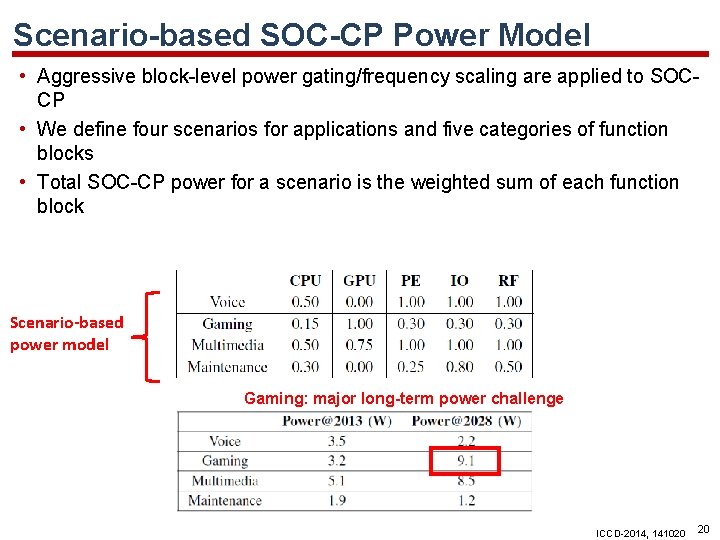
Scenario-based SOC-CP Power Model • Aggressive block-level power gating/frequency scaling are applied to SOCCP • We define four scenarios for applications and five categories of function blocks • Total SOC-CP power for a scenario is the weighted sum of each function block Scenario-based power model Gaming: major long-term power challenge ICCD-2014, 141020 20
![Function Block-Based Frequency Roadmap Frequency [GHz] • (WAS) All function blocks scale at the Function Block-Based Frequency Roadmap Frequency [GHz] • (WAS) All function blocks scale at the](http://slidetodoc.com/presentation_image_h/09786dcde0587bd230b17a6b69279140/image-21.jpg)
Function Block-Based Frequency Roadmap Frequency [GHz] • (WAS) All function blocks scale at the same frequency • (IS) Each block scale the frequency separately 8. 00 7. 00 6. 00 5. 00 4. 00 3. 00 2. 00 1. 00 0. 00 (IS) Main Processor [GHz] (IS) GPU [GHz] (IS) PE [GHz] (WAS) Main Processor / PE / Peripheral [GHz] 2013 2014 2015 2016 2017 2018 2019 2020 2021 2022 2023 2024 2025 2026 2027 2028 Year ICCD-2014, 141020 21
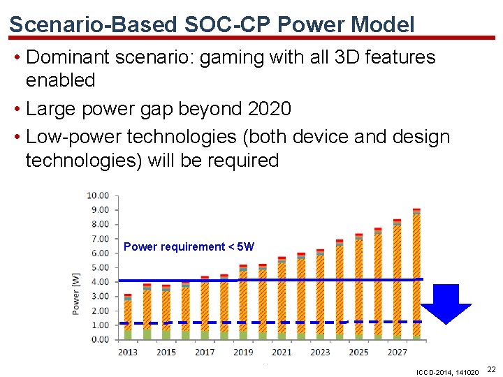
Scenario-Based SOC-CP Power Model • Dominant scenario: gaming with all 3 D features enabled • Large power gap beyond 2020 • Low-power technologies (both device and design technologies) will be required Power requirement < 5 W ICCD-2014, 141020 22
Outline • Overview of ITRS Design and System Drivers Chapters • Design Capacity Gap and Design Equivalent Scaling • Architectural and Area Models of MPU and SOC • Power Modeling and Power Management Gap • Conclusions ICCD-2014, 141020 23

Conclusions • SRAM and logic A-factors are updated with new calibration • Area models are updated with new A-factor, and new overhead models • Design Capability Gap stands between ideal density scaling and actual (realized) density scaling • DES is required to restore the scaling to the Moore’s Law track • Power model is updated with new frequency scaling, device parameters, and new transistor density models • We have shown the low-power design challenge with the scenario-based power model for SOC-CP ICCD-2014, 141020 24

Thank you! ICCD-2014, 141020 25

Backup ICCD-2014, 141020 26

Previous Challenge: Missing Node in Physical Scaling ISRealistic 450 One node missing 400 Solution: Alt-1 MPU Area exploration WAS IS (w/ 6 y-DES) IS (w/o DES) 350 300 Solution: Alt-2 Rescued by DES 250 2013 2014 2015 2016 2017 2018 2019 2020 2021 2022 2023 2024 2025 2026 2027 2028 Ideal WAS Die Area (mm^2) 45 40 35 30 25 20 15 10 5 0 2013 2014 2015 2016 2017 2018 2019 2020 2021 2022 2023 2024 2025 2026 2027 2028 M 1 HP (F) (nm) • Year ICCD-2014, 141020 27
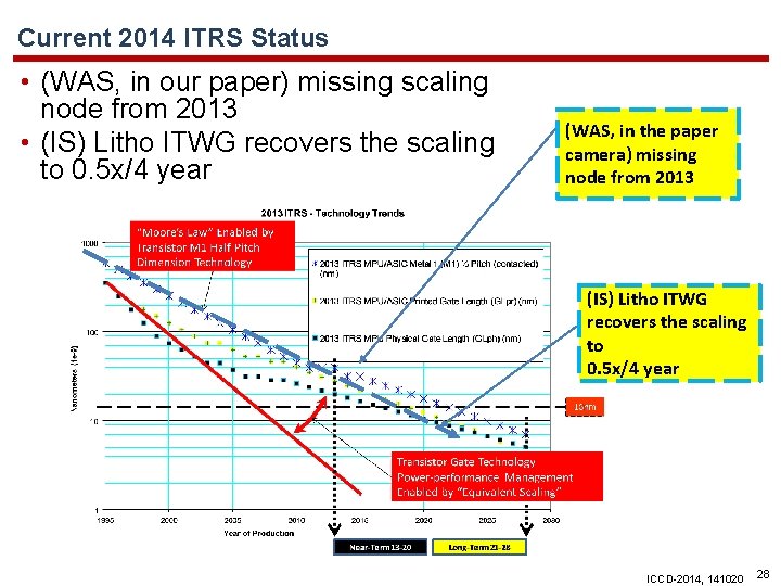
Current 2014 ITRS Status • (WAS, in our paper) missing scaling node from 2013 • (IS) Litho ITWG recovers the scaling to 0. 5 x/4 year (WAS, in the paper camera) missing node from 2013 (IS) Litho ITWG recovers the scaling to 0. 5 x/4 year ICCD-2014, 141020 28
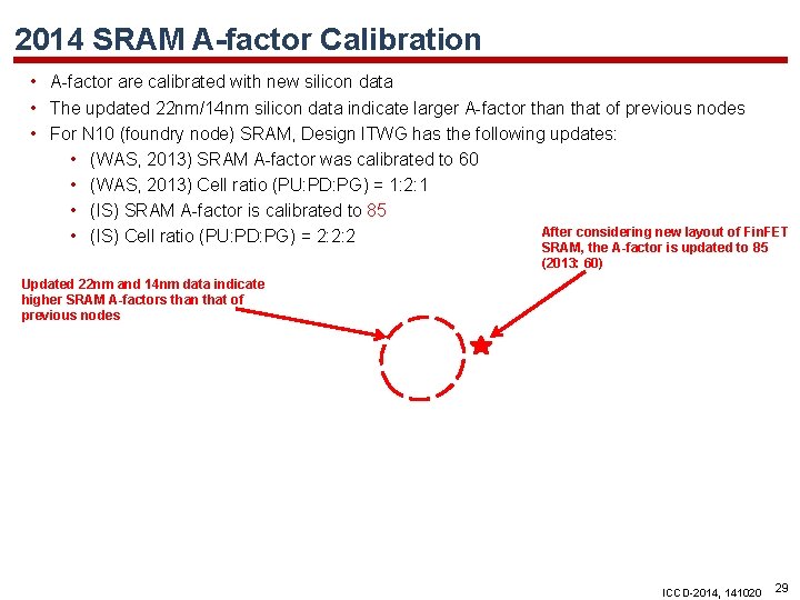
2014 SRAM A-factor Calibration • A-factor are calibrated with new silicon data • The updated 22 nm/14 nm silicon data indicate larger A-factor than that of previous nodes • For N 10 (foundry node) SRAM, Design ITWG has the following updates: • (WAS, 2013) SRAM A-factor was calibrated to 60 • (WAS, 2013) Cell ratio (PU: PD: PG) = 1: 2: 1 • (IS) SRAM A-factor is calibrated to 85 After considering new layout of Fin. FET • (IS) Cell ratio (PU: PD: PG) = 2: 2: 2 SRAM, the A-factor is updated to 85 (2013: 60) Updated 22 nm and 14 nm data indicate higher SRAM A-factors than that of previous nodes ICCD-2014, 141020 29

Calibration of A-factors with Silicon Data • Data extracted from products of major semiconductor manufacturers • Data collected up to 20 nm foundry node After calibration ICCD-2014, 141020 30
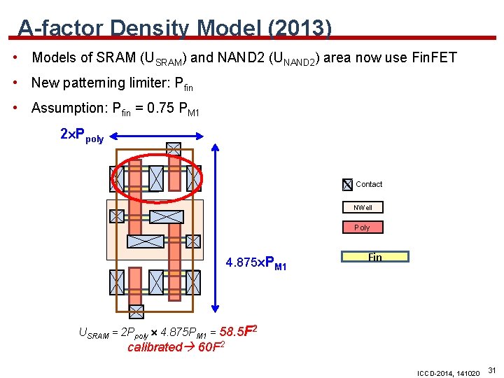
A-factor Density Model (2013) • Models of SRAM (USRAM) and NAND 2 (UNAND 2) area now use Fin. FET • New patterning limiter: Pfin • Assumption: Pfin = 0. 75 PM 1 2 Ppoly Contact NWell Poly Fin 4. 875 PM 1 USRAM = 2 Ppoly 4. 875 PM 1 = 58. 5 F 2 calibrated 60 F 2 ICCD-2014, 141020 31

A-factor Layout Model (2014) Assume Pfin = 0. 75 PM 1 Alt-1: ITRS 2013 / Intel 22 nm Fin. FET 6 T SRAM (1: 2: 1) Assume Ppoly = 1. 5 PM 1 Height = 2 Ppoly PG PD PU Width = 6. 5 Pfin Area = 2 Ppoly × 6. 5 Pfin PD PG PU = 58. 5 F 2 (similar to bulk) A-factor = 60 (after calibration) Assume Pfin = 0. 75 PM 1 Height Width Area = 2 Ppoly = 8. 5 Pfin = 2 Ppoly × 9. 5 Pfin = 85 F 2 (Intel 14 nm SRAM = 87 F 2) Alt-2: Fin. FET 6 T SRAM (1: 2: 1) (Intel 14 nm SRAM) PU PG PD 2 Ppoly PD 0. 75 Pfin 1 Pfin PU 2 Pfin PG 2 Pfin 1 Pfin 0. 75 Pfin ICCD-2014, 141020 32

Mission of ITRS Roadmap • http: //www. itrs. net/ • 15 -year technical outlook for 14 supplier industries and their respective technology areas • 25 -year projection of technology needs for emerging research devices and materials • Drivers for world wide research and funding agencies • Organization divided (EU, Japan, Korea, Taiwan, USA), 1000+ participants • Neutrality with regard to commercial considerations ICCD-2014, 141020 33

Interactions between ITWGs ORTCs INTC PIDS CM P, R , LITHO OL, Jma x Id, sat, Isd, leak CV/I, f. T Vt FEP C, M Design & System Drivers tion a i r va , 3σ D t, C y s o a c sk overl a M ch, pit #cores, max IO freq Test #IOs, max power, thermal, TSV/3 D roadmap Fundamental Models max chip power layout density transistor count chip size #distinct cores #cores max on-chip freq product/market drivers • • A&P ICCD-2014, 141020 34
![Intel MPU Scaling Trends # of Transistors Clock Frequency Power Performance/CLK (ILP) [Sutter 09] Intel MPU Scaling Trends # of Transistors Clock Frequency Power Performance/CLK (ILP) [Sutter 09]](http://slidetodoc.com/presentation_image_h/09786dcde0587bd230b17a6b69279140/image-35.jpg)
Intel MPU Scaling Trends # of Transistors Clock Frequency Power Performance/CLK (ILP) [Sutter 09] ICCD-2014, 141020 35
- Slides: 35