The CMS Silicon Pixel Detector for HLLHC Georg

- Slides: 23

The CMS Silicon Pixel Detector for HL-LHC Georg Steinbrück, Hamburg University for the CMS Collaboration Vertex 2016 September 25 -30, 2016 La Biodola, Isola d'Elba, Italy

Outline The CMS Tracking Detector Upgrade for the HL-LHC Detector layout Status of pixel sensor R&D Planar and 3 D silicon Serial powering Modules CMS Phase II Pixel Upgrade Georg Steinbrück georg. steinbrueck@desy. de 2

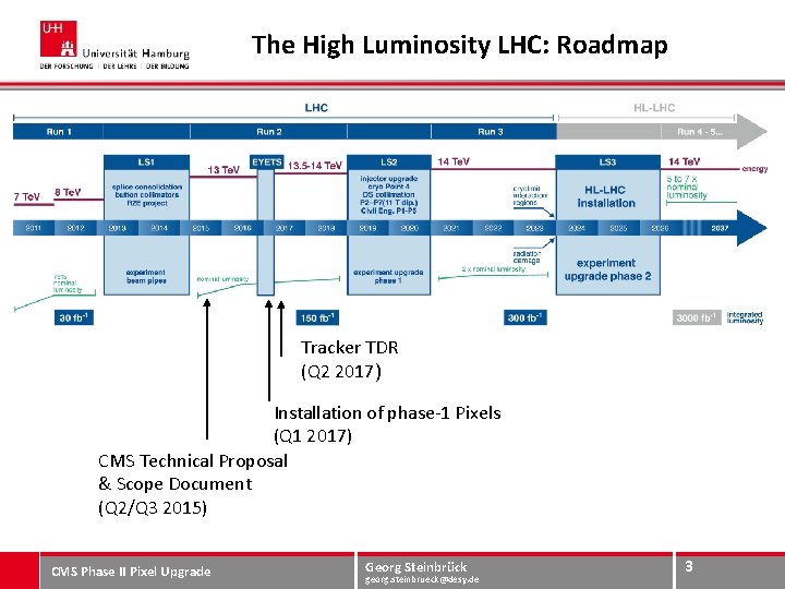
The High Luminosity LHC: Roadmap Tracker TDR (Q 2 2017) Installation of phase-1 Pixels (Q 1 2017) CMS Technical Proposal & Scope Document (Q 2/Q 3 2015) CMS Phase II Pixel Upgrade Georg Steinbrück georg. steinbrueck@desy. de 3

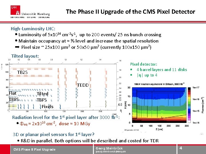
The Phase II Upgrade of the CMS Pixel Detector High-Luminosity LHC: • Luminosity of 5 x 1034 cm-2 s-1, up to 200 events/ 25 ns bunch crossing • Maintain occupancy at ≈ % level and increase the spatial resolution ➡ Pixel size ~ 25 x 100 μm 2 or 50 x 50 μm 2 (currently 100 x 150 μm 2) Tilted layout: Pixel detector: § 4 barrel layers and 11 disks § |η| up to 4 TB 2 S TEDD Flat TBPS Tilted TBPS Pixels Radiation level for the 1 st pixel layer after 3000 fb-1: • Φeq ≈ 2 x 1016 cm-2, dose ≈ 10 MGy 3 D or planar pixel sensors for 1 st layer? • R&D in parallel. Both options will be described and costed for TDR CMS Phase II Pixel Upgrade Georg Steinbrück georg. steinbrueck@desy. de 4 4

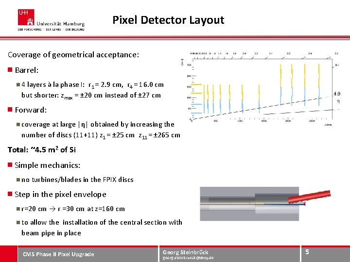
Pixel Detector Layout Coverage of geometrical acceptance: Barrel: 4 layers à la phase I: r 1 = 2. 9 cm, r 4 = 16. 0 cm but shorter: zmax = ± 20 cm instead of ± 27 cm Forward: coverage at large |η| obtained by increasing the number of discs (11+11) z 1 = ± 25 cm z 11 = ± 265 cm Total: ~4. 5 m 2 of Si Simple mechanics: no turbines/blades in the FPIX discs Step in the pixel envelope r=20 cm → r =30 cm at z=160 cm to allow the installation of the central section with beam pipe in place CMS Phase II Pixel Upgrade Georg Steinbrück georg. steinbrueck@desy. de 5 5

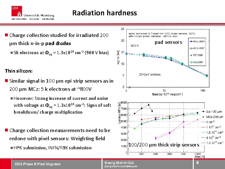
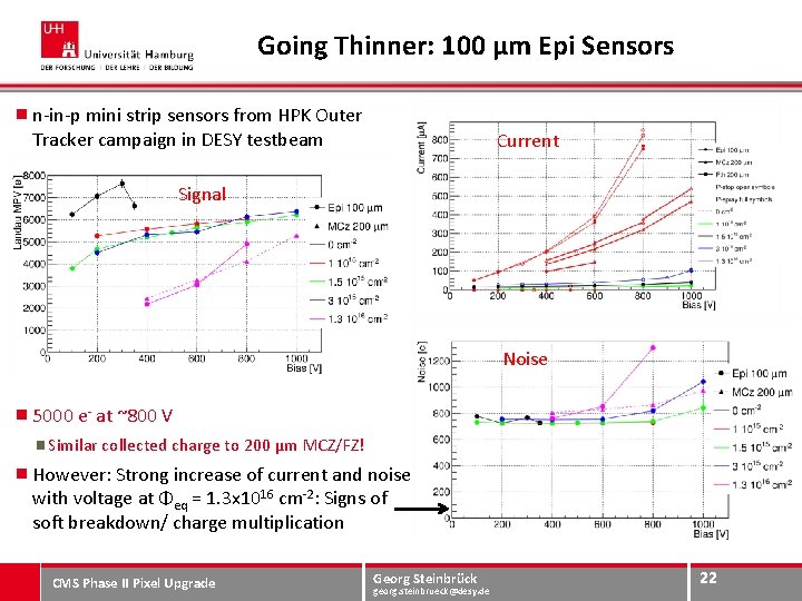
Radiation hardness Charge collection studied for irradiated 200 µm thick n-in-p pad diodes pad sensors 5 k electrons at Φeq = 1. 3 x 1016 cm-2 (900 V bias) Thin silicon: Similar signal in 100 µm epi strip sensors as in 200 µm MCz: 5 k electrons at ~800 V However: Strong increase of current and noise with voltage at Φeq = 1. 3 x 1016 cm-2: Signs of soft breakdown/ charge multiplication Charge collection measurements need to be redone with pixel sensors: Weighting field HPK submission, INFN/FBK submission CMS Phase II Pixel Upgrade 100/200 µm thick strip sensors Georg Steinbrück georg. steinbrueck@desy. de 6

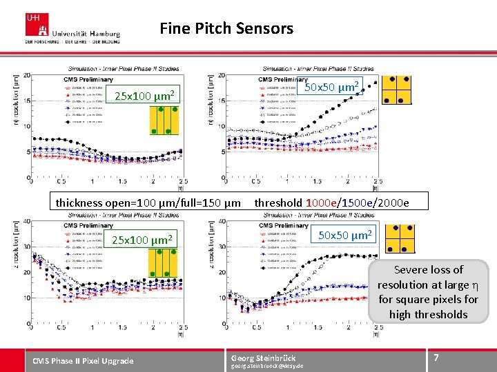
Fine Pitch Sensors 25 x 100 50 x 50 μm 2 thickness open=100 μm/full=150 μm threshold 1000 e/1500 e/2000 e 50 x 50 μm 2 25 x 100 μm 2 Severe loss of resolution at large h for square pixels for high thresholds CMS Phase II Pixel Upgrade Georg Steinbrück georg. steinbrueck@desy. de 7

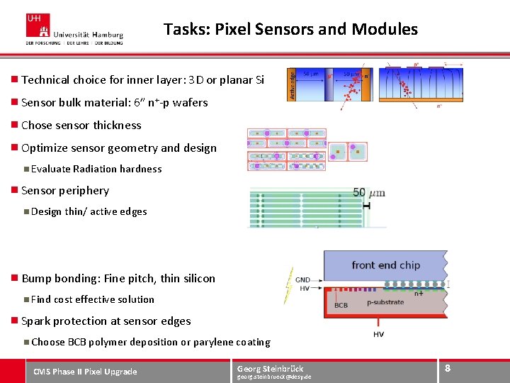
Tasks: Pixel Sensors and Modules Technical choice for inner layer: 3 D or planar Si Sensor bulk material: 6” n+-p wafers Chose sensor thickness Optimize sensor geometry and design Evaluate Radiation hardness Sensor periphery Design thin/ active edges Bump bonding: Fine pitch, thin silicon Find cost effective solution Spark protection at sensor edges Choose BCB polymer deposition or parylene coating CMS Phase II Pixel Upgrade Georg Steinbrück georg. steinbrueck@desy. de 8

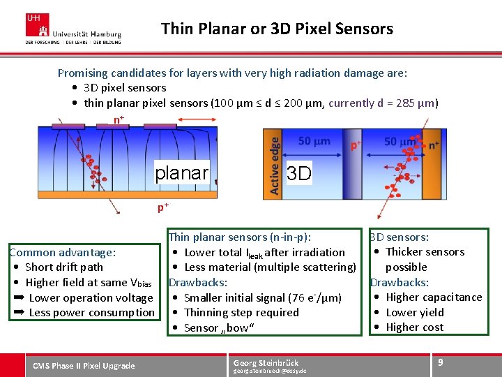
Thin Planar or 3 D Pixel Sensors Promising candidates for layers with very high radiation damage are: • 3 D pixel sensors • thin planar pixel sensors (100 μm ≤ d ≤ 200 μm, currently d = 285 μm) n+ planar 3 D p+ Common advantage: • Short drift path • Higher field at same Vbias ➡ Lower operation voltage ➡ Less power consumption CMS Phase II Pixel Upgrade Thin planar sensors (n-in-p): • Lower total Ileak after irradiation • Less material (multiple scattering) Drawbacks: • Smaller initial signal (76 e-/μm) • Thinning step required • Sensor „bow“ Georg Steinbrück georg. steinbrueck@desy. de 3 D sensors: • Thicker sensors possible Drawbacks: • Higher capacitance • Lower yield • Higher cost 9

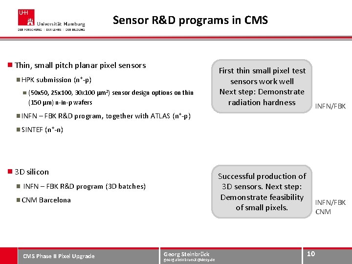
Sensor R&D programs in CMS Thin, small pitch planar pixel sensors HPK submission (n+-p) (50 x 50, 25 x 100, 30 x 100 µm 2) sensor design options on thin (150 µm) n-in-p wafers First thin small pixel test sensors work well Next step: Demonstrate radiation hardness INFN/FBK Successful production of 3 D sensors. Next step: Demonstrate feasibility of small pixels. INFN/FBK CNM INFN – FBK R&D program, together with ATLAS (n+-p) SINTEF (n+-n) 3 D silicon INFN – FBK R&D program (3 D batches) CNM Barcelona CMS Phase II Pixel Upgrade Georg Steinbrück georg. steinbrueck@desy. de 10

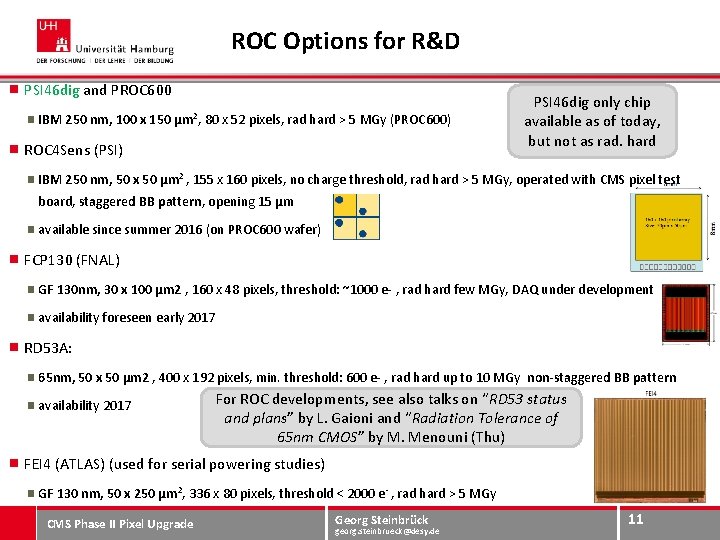
ROC Options for R&D PSI 46 dig and PROC 600 IBM 250 nm, 100 x 150 μm 2, 80 x 52 pixels, rad hard > 5 MGy (PROC 600) ROC 4 Sens (PSI) PSI 46 dig only chip available as of today, but not as rad. hard IBM 250 nm, 50 x 50 μm 2 , 155 x 160 pixels, no charge threshold, rad hard > 5 MGy, operated with CMS pixel test board, staggered BB pattern, opening 15 μm available since summer 2016 (on PROC 600 wafer) FCP 130 (FNAL) GF 130 nm, 30 x 100 μm 2 , 160 x 48 pixels, threshold: ~1000 e- , rad hard few MGy, DAQ under development availability foreseen early 2017 RD 53 A: 65 nm, 50 x 50 μm 2 , 400 x 192 pixels, min. threshold: 600 e- , rad hard up to 10 MGy non-staggered BB pattern availability 2017 For ROC developments, see also talks on “RD 53 status and plans” by L. Gaioni and “Radiation Tolerance of 65 nm CMOS” by M. Menouni (Thu) FEI 4 (ATLAS) (used for serial powering studies) GF 130 nm, 50 x 250 μm 2, 336 x 80 pixels, threshold < 2000 e- , rad hard > 5 MGy CMS Phase II Pixel Upgrade Georg Steinbrück georg. steinbrueck@desy. de 11

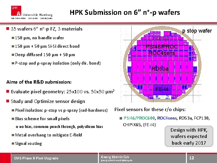
HPK Submission on 6” n+-p wafers 35 wafers 6” n+-p FZ, 3 materials p stop wafer 150 µm, no handle wafer FCP 130 150 µm + 50 µm Si-Si direct bond PSI 46/PROC 4 sens Deep diffused 150 µm + 50 µm P-stop and p-spray isolation (only dir. bond) RD 53 a Aims of the R&D submission: FE-I 4 Evaluate pixel geometry: 25 x 100 vs. 50 x 50 µm 2 Study and Optimize sensor design Pixel isolation: p-stop vs p-spray (rad-hardness) Bias scheme for small pixels no bias, common punch through, polysilicon bias Pixel sensors for these r/o chips: PSI 46/PROC 600, ROC 4 sens, RD 53 a, FCP 130, CHIPIX 65, (FE-I 4) Metal overhang to mitigate E-field Signal routing CMS Phase II Pixel Upgrade Georg Steinbrück georg. steinbrueck@desy. de Design with HPK, wafers expected back early 2017 12

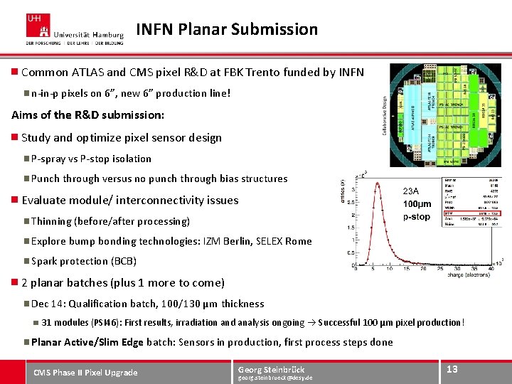
INFN Planar Submission Common ATLAS and CMS pixel R&D at FBK Trento funded by INFN n-in-p pixels on 6”, new 6” production line! Aims of the R&D submission: Study and optimize pixel sensor design P-spray vs P-stop isolation Punch through versus no punch through bias structures Evaluate module/ interconnectivity issues Thinning (before/after processing) Explore bump bonding technologies: IZM Berlin, SELEX Rome Spark protection (BCB) 2 planar batches (plus 1 more to come) Dec 14: Qualification batch, 100/130 µm thickness 31 modules (PSI 46): First results, irradiation and analysis ongoing Successful 100 µm pixel production! Planar Active/Slim Edge batch: Sensors in production, first process steps done CMS Phase II Pixel Upgrade Georg Steinbrück georg. steinbrueck@desy. de 13

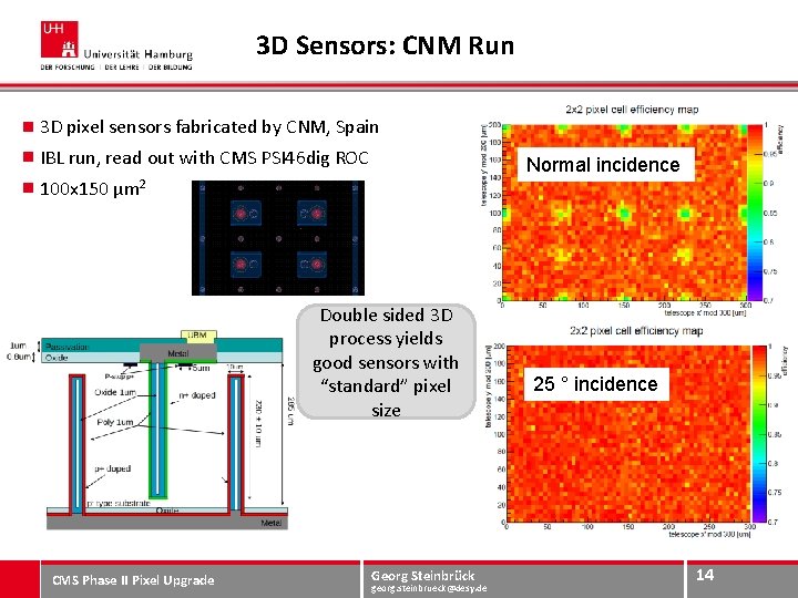
3 D Sensors: CNM Run 3 D pixel sensors fabricated by CNM, Spain IBL run, read out with CMS PSI 46 dig ROC Normal incidence 100 x 150 µm 2 Double sided 3 D process yields good sensors with “standard” pixel size CMS Phase II Pixel Upgrade Georg Steinbrück georg. steinbrueck@desy. de 25 ° incidence 14

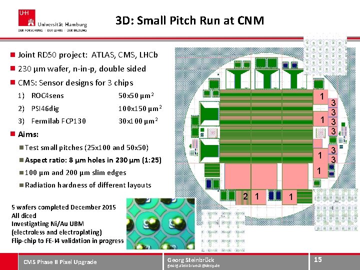
3 D: Small Pitch Run at CNM Joint RD 50 project: ATLAS, CMS, LHCb 230 µm wafer, n-in-p, double sided CMS: Sensor designs for 3 chips 1) ROC 4 sens 50 x 50 µm 2 2) PSI 46 dig 100 x 150 µm 2 3) Fermilab FCP 130 30 x 100 µm 2 1 3 3 Aims: Test small pitches (25 x 100 and 50 x 50) 3 1 Aspect ratio: 8 µm holes in 230 µm (1: 25) 100 µm and 200 µm slim edges Radiation hardness of different layouts 2 1 1 5 wafers completed December 2015 All diced Investigating Ni/Au UBM (electroless and electroplating) Flip-chip to FE-I 4 validation in progress CMS Phase II Pixel Upgrade Georg Steinbrück georg. steinbrueck@desy. de 15

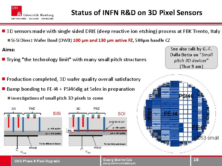
Status of INFN R&D on 3 D Pixel Sensors 3 D sensors made with single sided DRIE (deep reactive ion etching) process at FBK Trento, Italy Si-Si Direct Wafer Bond (DWB) 100 µm and 130 µm active FZ, 500µm handle CZ Aims: Trying "the technology limit" with many small pitch structures See also talk by G. -F. Dalla Betta on “Small pitch 3 D devices” (Thur 9 am) Production completed, 3 D wafer quality overall satisfactory Bump bonding to FE-I 4 + PSI 46 dig at Selex in preparation PSI 46 strips Investigations of small pitch 3 D pixels to come FE-I 4 FE-I 3 RD 53 small CMS Phase II Pixel Upgrade Georg Steinbrück georg. steinbrueck@desy. de 16

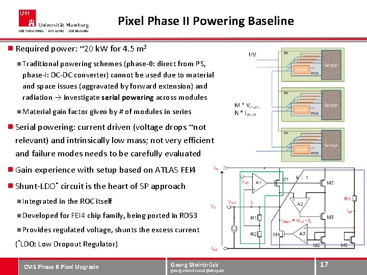
Pixel Phase II Powering Baseline Required power: ~20 k. W for 4. 5 m 2 Traditional powering schemes (phase-0: direct from PS, phase-I: DC-DC converter) cannot be used due to material and space issues (aggravated by forward extension) and radiation → investigate serial powering across modules Material gain factor given by # of modules in series Serial powering: current driven (voltage drops ~not relevant) and intrinsically low mass; not very efficient and failure modes needs to be carefully evaluated Gain experience with setup based on ATLAS FEI 4 Shunt-LDO* circuit is the heart of SP approach Integrated in the ROC itself Developed for FEI 4 chip family, being ported in RD 53 Provides regulated voltage, shunts the excess current (*LDO: Low Dropout Regulator) CMS Phase II Pixel Upgrade Georg Steinbrück georg. steinbrueck@desy. de 17

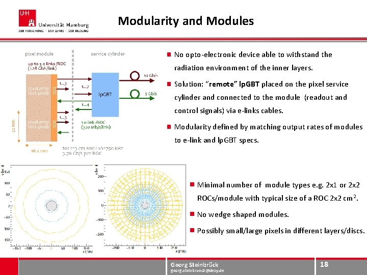
Modularity and Modules No opto-electronic device able to withstand the radiation environment of the inner layers. Solution: “remote” lp. GBT placed on the pixel service cylinder and connected to the module (readout and control signals) via e-links cables. Modularity defined by matching output rates of modules to e-link and lp. GBT specs. Minimal number of module types e. g. 2 x 1 or 2 x 2 ROCs/module with typical size of a ROC 2 x 2 cm 2. No wedge shaped modules. Possibly small/large pixels in different layers/discs. CMS Phase II Pixel Upgrade Georg Steinbrück georg. steinbrueck@desy. de 18

Conclusion HL-LHC poses high demands on pixel detector Radiation hardness thin sensors with radiation hard design Efficient and precise tracking at high rates small pixel pitches Radiation tolerant, fine pitch, low noise readout chips RD 53 Fast links R&D programs to develop thin, fine pitch sensors and address pixel design issues Planar: HPK submission, INFN/FBK (together with ATLAS), SINTEF 3 D: INFN/FBK (together with ATLAS), CNM Fine pitch bump bonding of thin sensors/ROCs challenging and a major cost driver Serial Powering baseline, R&D ongoing Tracker Upgrade TDR due next year! CMS Phase II Pixel Upgrade Georg Steinbrück georg. steinbrueck@desy. de 19

BACKUP CMS Phase II Pixel Upgrade Georg Steinbrück georg. steinbrueck@desy. de 20

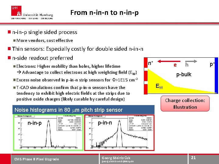
From n-in-n to n-in-p single sided process More vendors, cost effective Thin sensors: Especially costly for double sided n-in-n n-side readout preferred Electrons: Higher mobility than holes, higher lifetime Advantage to collect electrons at high weighting field (EW) n+ E e Noise histograms in 80 mm pitch strip sensor n-in-p CMS Phase II Pixel Upgrade EEWW・E EW Charge collection: Illustration p-in-n Georg Steinbrück georg. steinbrueck@desy. de p+ n-bulk p-bulk Excess noise observed in p-in-n strip sensors for F>1 E 15 cm-2 T-CAD simulations confirm that p-in-n sensors have the tendency to exhibit high electric fields at the strips due to positive oxide charges (likely curable by careful design) h 21 E

Going Thinner: 100 µm Epi Sensors n-in-p mini strip sensors from HPK Outer Tracker campaign in DESY testbeam Current Signal Noise 5000 e- at ~800 V Similar collected charge to 200 µm MCZ/FZ! However: Strong increase of current and noise with voltage at Φeq = 1. 3 x 1016 cm-2: Signs of soft breakdown/ charge multiplication CMS Phase II Pixel Upgrade Georg Steinbrück georg. steinbrueck@desy. de 22

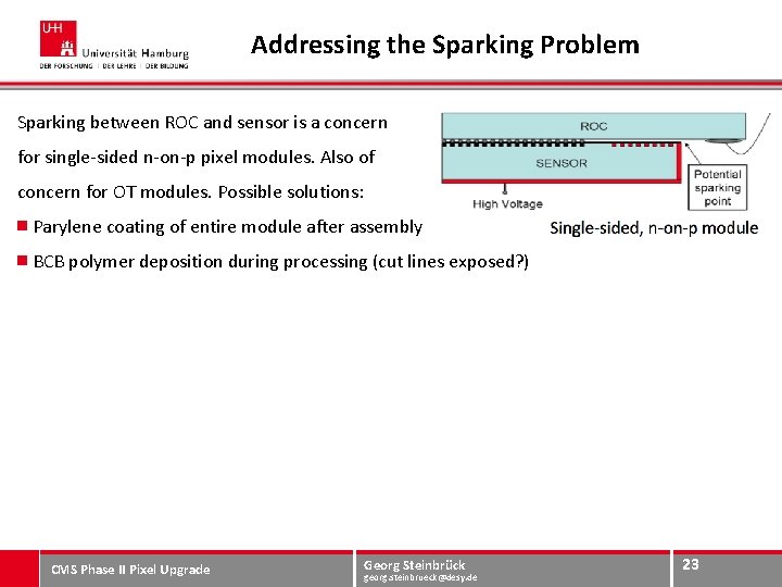
Addressing the Sparking Problem Sparking between ROC and sensor is a concern for single-sided n-on-p pixel modules. Also of concern for OT modules. Possible solutions: Parylene coating of entire module after assembly BCB polymer deposition during processing (cut lines exposed? ) CMS Phase II Pixel Upgrade Georg Steinbrück georg. steinbrueck@desy. de 23