CMS Pixel Simulation Quarter pixel Electrostatic potential Vincenzo

- Slides: 33

CMS Pixel Simulation Quarter pixel: Electrostatic potential Vincenzo Chiochia Physik Institut der Universität Zürich-Irchel CH-8057 Zürich (Switzerland) PIXEL 2005 Workshop Chuzenji Lake, Nikko (Japan) November 7 -11, 2005

Outline 1. 2. 3. 4. 5. The CMS pixel detector Radiation damage and impact on reconstruction Beam test data and detailed sensor simulation Physical modelling of radiation damage: a) Models with a constant space charge density b) Double-trap models Fluence and temperature dependence V. Chiochia – CMS Pixel Simulation – Vertex 2005 - Chuzenji Lake, Nikko, Japan , November 7 -11, 2005 2

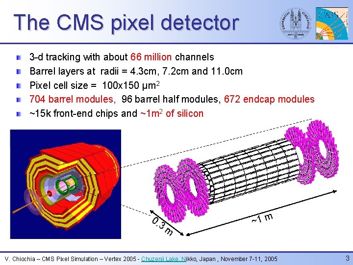
The CMS pixel detector 3 -d tracking with about 66 million channels Barrel layers at radii = 4. 3 cm, 7. 2 cm and 11. 0 cm Pixel cell size = 100 x 150 µm 2 704 barrel modules, 96 barrel half modules, 672 endcap modules ~15 k front-end chips and ~1 m 2 of silicon 0. 3 m ~1 m V. Chiochia – CMS Pixel Simulation – Vertex 2005 - Chuzenji Lake, Nikko, Japan , November 7 -11, 2005 3

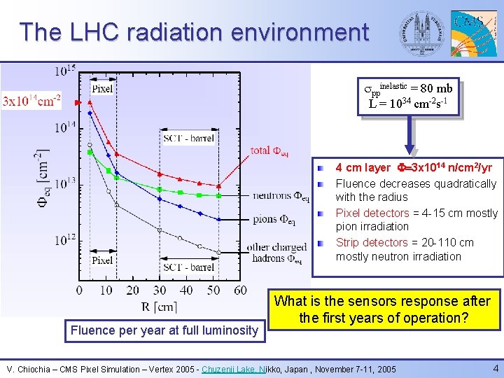
The LHC radiation environment sppinelastic = 80 mb L = 1034 cm-2 s-1 4 cm layer F=3 x 10¹⁴ n/cm 2/yr Fluence decreases quadratically with the radius Pixel detectors = 4 -15 cm mostly pion irradiation Strip detectors = 20 -110 cm mostly neutron irradiation Fluence per year at full luminosity What is the sensors response after the first years of operation? V. Chiochia – CMS Pixel Simulation – Vertex 2005 - Chuzenji Lake, Nikko, Japan , November 7 -11, 2005 4

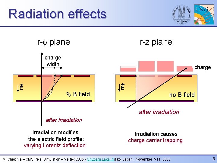
Radiation effects r-f plane r-z plane charge width E charge E B field no B field after irradiation Irradiation modifies the electric field profile: varying Lorentz deflection Irradiation causes charge carrier trapping V. Chiochia – CMS Pixel Simulation – Vertex 2005 - Chuzenji Lake, Nikko, Japan , November 7 -11, 2005 5

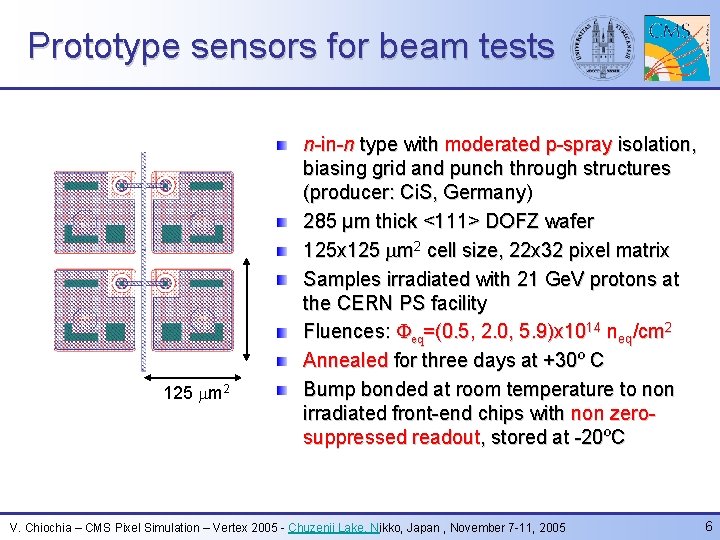
Prototype sensors for beam tests 125 m 2 n-in-n type with moderated p-spray isolation, biasing grid and punch through structures (producer: Ci. S, Germany) 285 μm thick <111> DOFZ wafer 125 x 125 m 2 cell size, 22 x 32 pixel matrix Samples irradiated with 21 Ge. V protons at the CERN PS facility Fluences: Feq=(0. 5, 2. 0, 5. 9)x 1014 neq/cm 2 Annealed for three days at +30º C Bump bonded at room temperature to non irradiated front-end chips with non zerosuppressed readout, stored at -20ºC V. Chiochia – CMS Pixel Simulation – Vertex 2005 - Chuzenji Lake, Nikko, Japan , November 7 -11, 2005 6

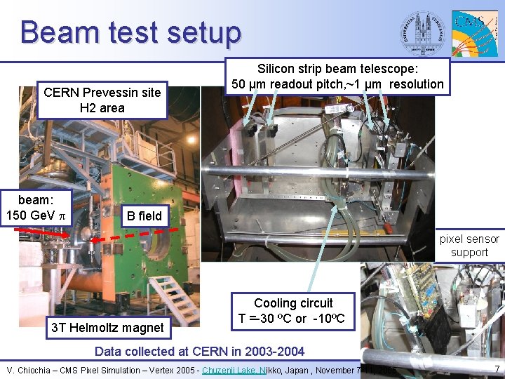
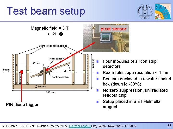
Beam test setup CERN Prevessin site H 2 area beam: 150 Ge. V p Silicon strip beam telescope: 50 μm readout pitch, ~1 μm resolution B field pixel sensor support 3 T Helmoltz magnet Cooling circuit T =-30 ºC or -10ºC Data collected at CERN in 2003 -2004 V. Chiochia – CMS Pixel Simulation – Vertex 2005 - Chuzenji Lake, Nikko, Japan , November 7 -11, 2005 7

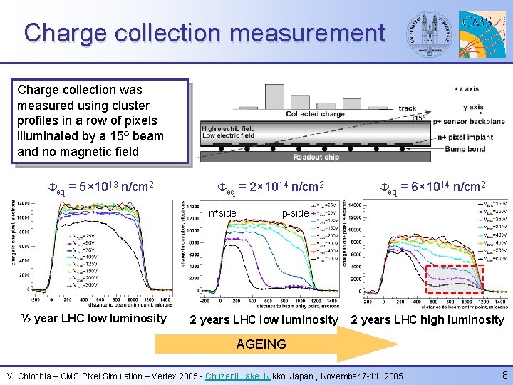
Charge collection measurement Charge collection was measured using cluster profiles in a row of pixels illuminated by a 15º beam and no magnetic field Feq = 5× 10¹³ n/cm 2 Feq = 2× 10¹⁴ n/cm 2 n+side ½ year LHC low luminosity Feq = 6× 10¹⁴ n/cm 2 p-side 2 years LHC low luminosity 2 years LHC high luminosity AGEING V. Chiochia – CMS Pixel Simulation – Vertex 2005 - Chuzenji Lake, Nikko, Japan , November 7 -11, 2005 8

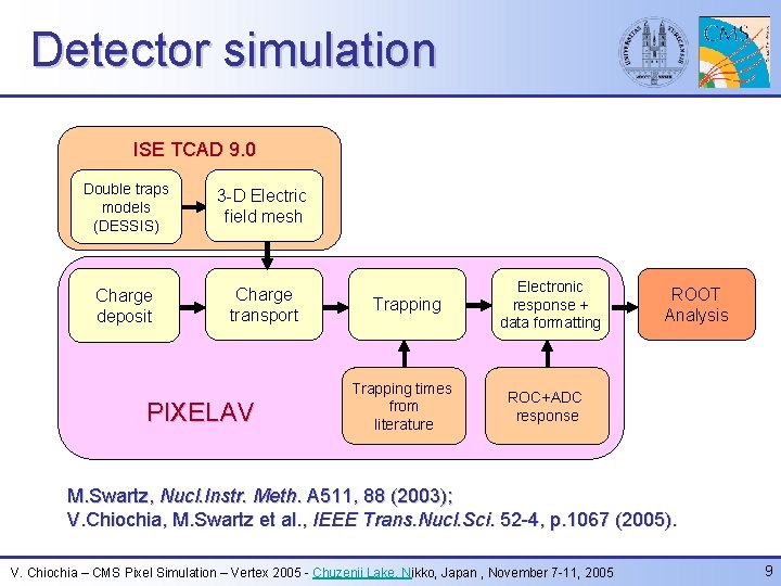
Detector simulation ISE TCAD 9. 0 Double traps models (DESSIS) 3 -D Electric field mesh Charge deposit Charge transport PIXELAV Trapping times from literature Electronic response + data formatting ROOT Analysis ROC+ADC response M. Swartz, Nucl. Instr. Meth. A 511, 88 (2003); V. Chiochia, M. Swartz et al. , IEEE Trans. Nucl. Sci. 52 -4, p. 1067 (2005). V. Chiochia – CMS Pixel Simulation – Vertex 2005 - Chuzenji Lake, Nikko, Japan , November 7 -11, 2005 9

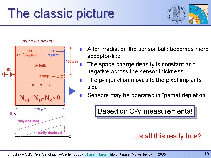
The classic picture after type inversion Neff=ND-NA<0 - After irradiation the sensor bulk becomes more acceptor-like The space charge density is constant and negative across the sensor thickness The p-n junction moves to the pixel implants side Sensors may be operated in “partial depletion” Based on C-V measurements! …is all this really true? V. Chiochia – CMS Pixel Simulation – Vertex 2005 - Chuzenji Lake, Nikko, Japan , November 7 -11, 2005 10

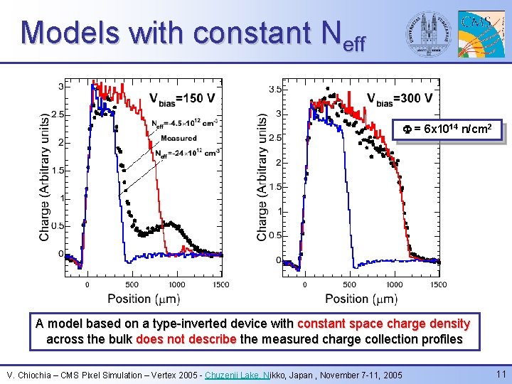
Models with constant Neff F = 6 x 10¹⁴ n/cm 2 A model based on a type-inverted device with constant space charge density across the bulk does not describe the measured charge collection profiles V. Chiochia – CMS Pixel Simulation – Vertex 2005 - Chuzenji Lake, Nikko, Japan , November 7 -11, 2005 11

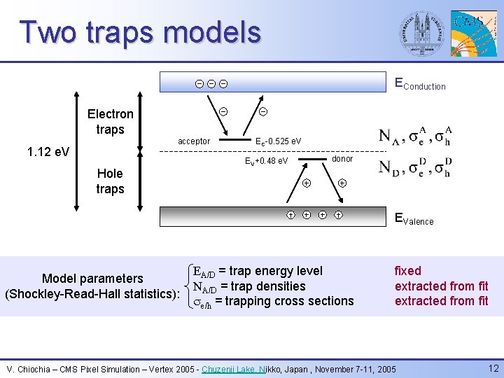
Two traps models EConduction Electron traps acceptor 1. 12 e. V Hole traps EC-0. 525 e. V EV+0. 48 e. V donor EValence Model parameters (Shockley-Read-Hall statistics): EA/D = trap energy level NA/D = trap densities se/h = trapping cross sections fixed extracted from fit V. Chiochia – CMS Pixel Simulation – Vertex 2005 - Chuzenji Lake, Nikko, Japan , November 7 -11, 2005 12

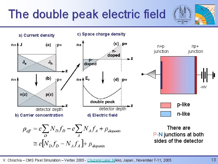
The double peak electric field a) Current density c) Space charge density n+p junction np+ junction -HV detector depth b) Carrier concentration p-like detector depth d) Electric field n-like There are P-N junctions at both sides of the detector V. Chiochia – CMS Pixel Simulation – Vertex 2005 - Chuzenji Lake, Nikko, Japan , November 7 -11, 2005 13

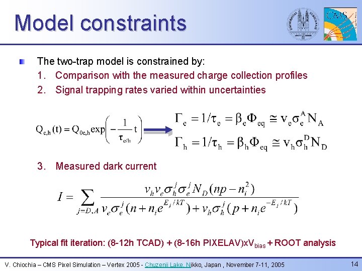
Model constraints The two-trap model is constrained by: 1. Comparison with the measured charge collection profiles 2. Signal trapping rates varied within uncertainties 3. Measured dark current Typical fit iteration: (8 -12 h TCAD) + (8 -16 h PIXELAV)x. Vbias + ROOT analysis V. Chiochia – CMS Pixel Simulation – Vertex 2005 - Chuzenji Lake, Nikko, Japan , November 7 -11, 2005 14

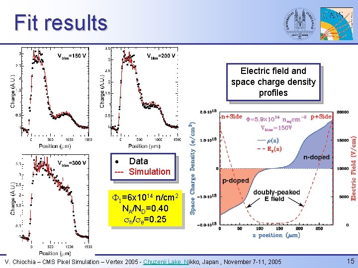
Fit results Electric field and space charge density profiles · Data --- Simulation F 1=6 x 10¹⁴ n/cm 2 NA/ND=0. 40 sh/se=0. 25 V. Chiochia – CMS Pixel Simulation – Vertex 2005 - Chuzenji Lake, Nikko, Japan , November 7 -11, 2005 15

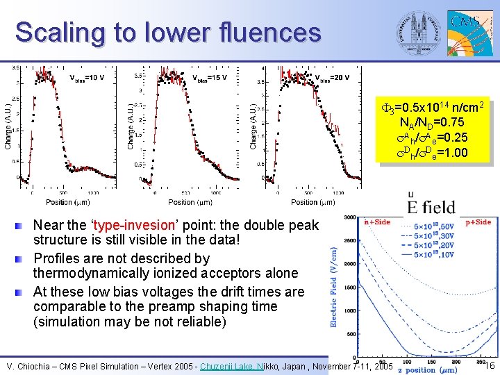
Scaling to lower fluences F 3=0. 5 x 10¹⁴ n/cm 2 NA/ND=0. 75 s. Ah/s. Ae=0. 25 s. Dh/s. De=1. 00 Near the ‘type-invesion’ point: the double peak structure is still visible in the data! Profiles are not described by thermodynamically ionized acceptors alone At these low bias voltages the drift times are comparable to the preamp shaping time (simulation may be not reliable) V. Chiochia – CMS Pixel Simulation – Vertex 2005 - Chuzenji Lake, Nikko, Japan , November 7 -11, 2005 16

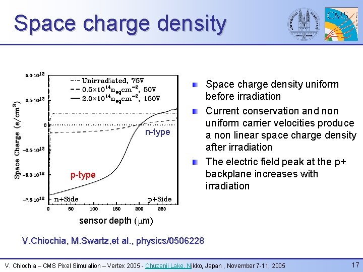
Space charge density n-type p-type Space charge density uniform before irradiation Current conservation and non uniform carrier velocities produce a non linear space charge density after irradiation The electric field peak at the p+ backplane increases with irradiation sensor depth ( m) V. Chiochia, M. Swartz, et al. , physics/0506228 V. Chiochia – CMS Pixel Simulation – Vertex 2005 - Chuzenji Lake, Nikko, Japan , November 7 -11, 2005 17

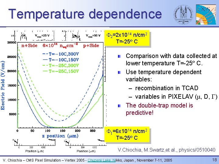
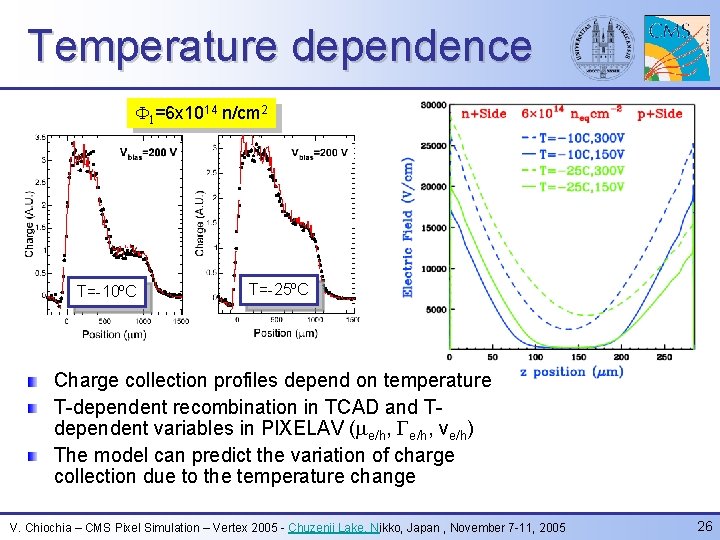
Temperature dependence F 2=2 x 10¹⁴ n/cm 2 T=-25º C Comparison with data collected at lower temperature T=-25º C. Use temperature dependent variables: – recombination in TCAD – variables in PIXELAV ( , D, G) The double-trap model is predictive! F 1=6 x 10¹⁴ n/cm 2 T=-25º C V. Chiochia, M. Swartz, et al. , physics/0510040 V. Chiochia – CMS Pixel Simulation – Vertex 2005 - Chuzenji Lake, Nikko, Japan , November 7 -11, 2005 18

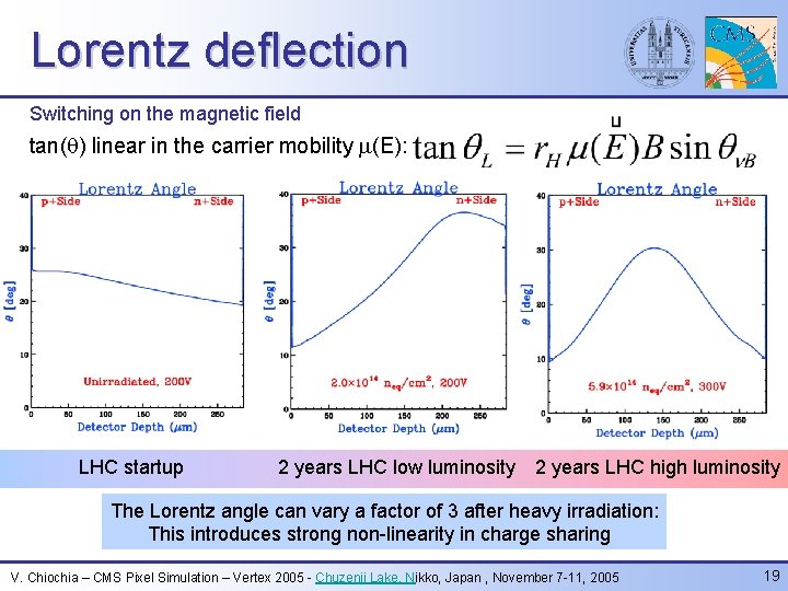
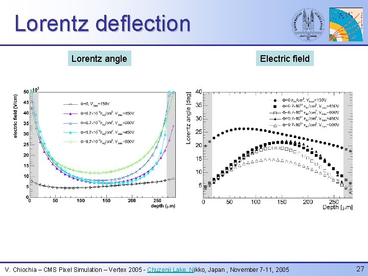
Lorentz deflection Switching on the magnetic field tan( ) linear in the carrier mobility (E): LHC startup 2 years LHC low luminosity 2 years LHC high luminosity The Lorentz angle can vary a factor of 3 after heavy irradiation: This introduces strong non-linearity in charge sharing V. Chiochia – CMS Pixel Simulation – Vertex 2005 - Chuzenji Lake, Nikko, Japan , November 7 -11, 2005 19

Conclusions and plans After heavy irradiation trapping of the leakage current produces electric field profiles with two maxima at the detector implants. The space charge density across the sensor is not uniform. What is the meaning of Vdep, depletion depth and type inversion? Measurements reflecting the electric field profile (e. g. TCT, CCE, long clusters etc. ) are preferable to C-V characterization to understand radiation damage in running detectors A physical model based on two defect levels can describe the charge collection profiles measured with irradiated pixel sensors in the whole range of irradiation fluences relevant to LHC operation Our model is an effective theory: e. g. in reality there are several trap levels in the silicon band gap after irradiation. However, it is suited for applications related to silicon detector operation at LHC. We are currently using the PIXELAV simulation to develop hit reconstruction algorithms optimized for irradiated pixel sensors. V. Chiochia – CMS Pixel Simulation – Vertex 2005 - Chuzenji Lake, Nikko, Japan , November 7 -11, 2005 20

References PIXELAV simulation: – M. Swartz, “CMS Pixel simulations”, Nucl. Instr. Meth. A 511, 88 (2003) Double-trap model: – V. Chiochia, M. Swartz et al. , “Simulation of Heavily Irradiated Silicon Pixel Sensors and Comparison with Test Beam Measurements”, IEEE Trans. Nucl. Sci. 52 -4, p. 1067 (2005), eprint: physics/0411143 – V. Eremin, E. Verbitskaya, and Z. Li, “The origin of double peak electric field distribution in heavily irradiated silicon detectors”, Nucl. Instr. Meth. A 476, pp. 556 -564 (2002) Model fluence and temperature dependence: – V. Chiochia, M. Swartz et al. , “A double junction model of irradiated pixel sensors for LHC”, submitted to Nucl. Instr. Meth. , eprint: physics/0506228 – V. Chiochia, M. Swartz et al. , “Observation, modeling, and temperature dependence of doubly-peaked electric fields in silicon pixel sensors”, submitted to Nucl. Instr. Meth. , eprint: physics/0510040 V. Chiochia – CMS Pixel Simulation – Vertex 2005 - Chuzenji Lake, Nikko, Japan , November 7 -11, 2005 21

Backup slides 22

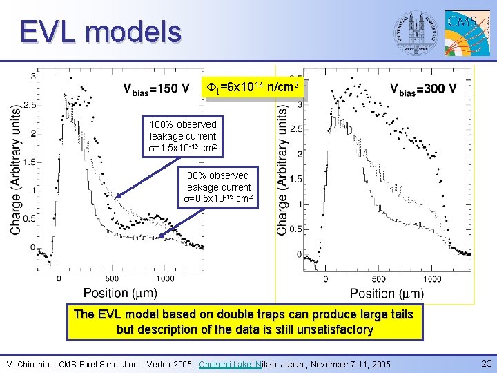
EVL models F 1=6 x 10¹⁴ n/cm 2 100% observed leakage current s=1. 5 x 10 -15 cm 2 30% observed leakage current s=0. 5 x 10 -15 cm 2 The EVL model based on double traps can produce large tails but description of the data is still unsatisfactory V. Chiochia – CMS Pixel Simulation – Vertex 2005 - Chuzenji Lake, Nikko, Japan , November 7 -11, 2005 23

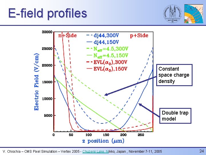
E-field profiles Constant space charge density Double trap model V. Chiochia – CMS Pixel Simulation – Vertex 2005 - Chuzenji Lake, Nikko, Japan , November 7 -11, 2005 24

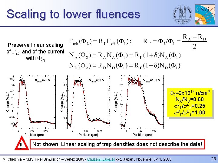
Scaling to lower fluences Preserve linear scaling of Ge/h and of the current with Feq F 2=2 x 10¹⁴ n/cm 2 NA/ND=0. 68 s. Ah/s. Ae=0. 25 s. Dh/s. De=1. 00 ! Not shown: Linear scaling of trap densities does not describe the data! V. Chiochia – CMS Pixel Simulation – Vertex 2005 - Chuzenji Lake, Nikko, Japan , November 7 -11, 2005 25

Temperature dependence F 1=6 x 10¹⁴ n/cm 2 T=-10ºC T=-25ºC Charge collection profiles depend on temperature T-dependent recombination in TCAD and Tdependent variables in PIXELAV ( e/h, Ge/h, ve/h) The model can predict the variation of charge collection due to the temperature change V. Chiochia – CMS Pixel Simulation – Vertex 2005 - Chuzenji Lake, Nikko, Japan , November 7 -11, 2005 26

Lorentz deflection Lorentz angle Electric field V. Chiochia – CMS Pixel Simulation – Vertex 2005 - Chuzenji Lake, Nikko, Japan , November 7 -11, 2005 27

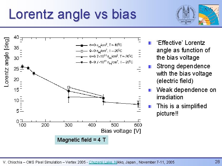
Lorentz angle vs bias ‘Effective’ Lorentz angle as function of the bias voltage Strong dependence with the bias voltage (electric field) Weak dependence on irradiation This is a simplified picture!! Magnetic field = 4 T V. Chiochia – CMS Pixel Simulation – Vertex 2005 - Chuzenji Lake, Nikko, Japan , November 7 -11, 2005 28

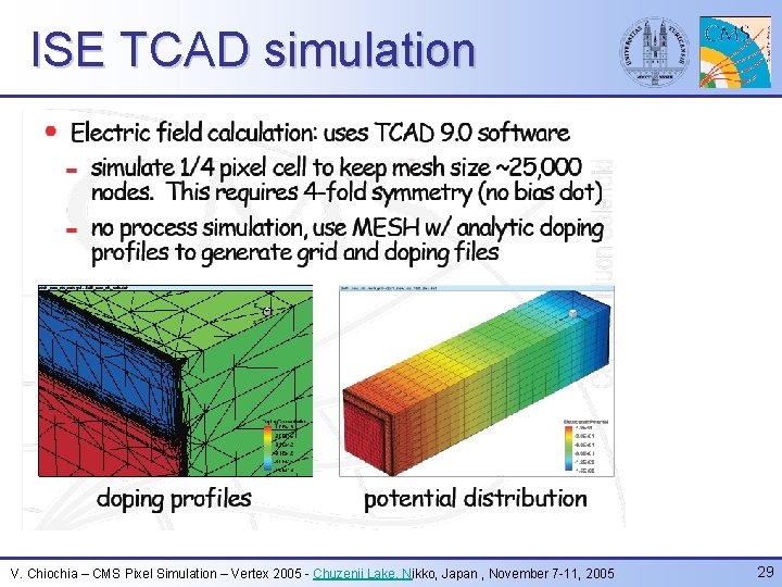
ISE TCAD simulation V. Chiochia – CMS Pixel Simulation – Vertex 2005 - Chuzenji Lake, Nikko, Japan , November 7 -11, 2005 29

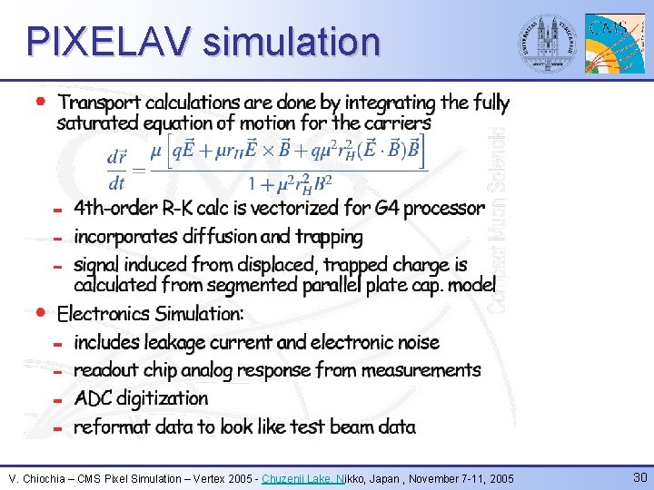
PIXELAV simulation V. Chiochia – CMS Pixel Simulation – Vertex 2005 - Chuzenji Lake, Nikko, Japan , November 7 -11, 2005 30

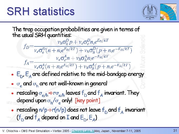
SRH statistics V. Chiochia – CMS Pixel Simulation – Vertex 2005 - Chuzenji Lake, Nikko, Japan , November 7 -11, 2005 31

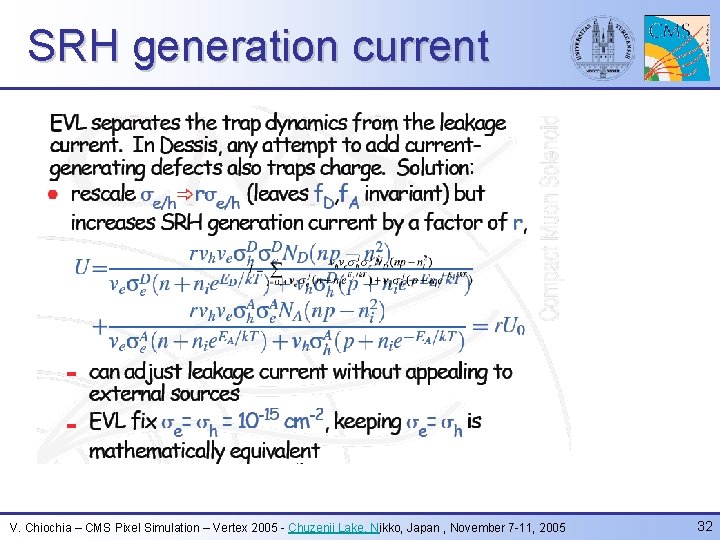
SRH generation current V. Chiochia – CMS Pixel Simulation – Vertex 2005 - Chuzenji Lake, Nikko, Japan , November 7 -11, 2005 32

Test beam setup Magnetic field = 3 T or PIN diode trigger pixel sensor Four modules of silicon strip detectors Beam telescope resolution ~ 1 m Sensors enclosed in a water cooled box (down to -30ºC) No zero suppression, unirradiated readout chip Setup placed in a 3 T Helmoltz magnet V. Chiochia – CMS Pixel Simulation – Vertex 2005 - Chuzenji Lake, Nikko, Japan , November 7 -11, 2005 33