SIMD Single instruction on multiple data has existed


")
 or clock")


![Handling If Statements • Consider – for(i=0; i<n; i++) – if(x[i] != 0) –](https://slidetodoc.com/presentation_image_h2/ea8529870521fa4d54534c2a232334cd/image-14.jpg "Handling If Statements • Consider – for(i=0; i<n; i++) – if(x[i] != 0) –")
 vsetpcfgi")


 thousands of parallel FP units – GPUs did")

; // daxpy code in")


")


![Continued • Let’s first consider this by an example – if(X[i]!=0) X[i]=X[i]-Y[i]; else X[i]=Z[i];](https://slidetodoc.com/presentation_image_h2/ea8529870521fa4d54534c2a232334cd/image-35.jpg "Continued • Let’s first consider this by an example – if(X[i]!=0) X[i]=X[i]-Y[i]; else X[i]=Z[i];")
![CUDA Code for if-else ld. global. f 64 RD 0, [X+R 8] // load](https://slidetodoc.com/presentation_image_h2/ea8529870521fa4d54534c2a232334cd/image-36.jpg "CUDA Code for if-else ld. global. f 64 RD 0, [X+R 8] // load")


- Slides: 44
SIMD • Single instruction on multiple data – has existed since the 1960 s – execute array operations parallel on different processing elements (ALUs) (rather than looping) • convert for(i=0; i<n; i++) a[i]++; • into a single operation, say A=A+1 – we get a speedup from the parallelism but also from removing the loop mechanisms • incrementing i, comparison and conditional branch • 3 approaches to SIMD – vector architectures (including matrix architectures) – multimedia SIMD instruction set extensions – graphics processor units
Two Views • CPU divided into control unit and n processing elements – each PE handles 1 datum from the array on the given operation – data are cached in local caches (one per PE) • Pipelined functional units – issue instruction on different array values sequentially to the same functional unit – FU is pipelined, each array element is processed in an overlapped fashion in the pipelined FU – requires accessing vector element every clock cycle (from register or cache)
The Pipelined Approach • The first approach is much more efficient but not realistic – an array of 1000 values requires 1000 PEs and 1000 local caches • Using pipelined functional units costs almost nothing – with vector operations, we can still eliminate the looping mechanism as long as the size of the registers storing our vectors can store the entire vector at one time (otherwise, we still need a loop) – using multi-banked caches improves performance so that multiple loads/stores can take place per cycle – requires less power utilization
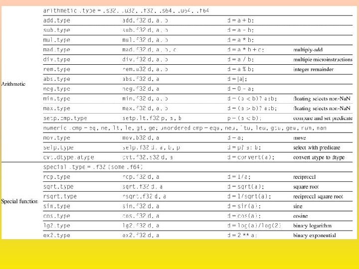
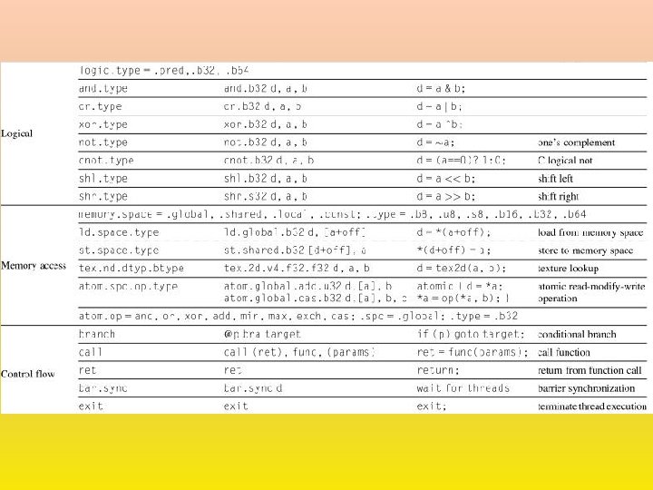
RV 64 V • A vector-based version of RISC-V – based loosely on the Cray-1 supercomputer (1970 s) • Operations are – scalar – operate on scalar registers but still use pipelined functional unit – vector – operate on vector register and scalar register – matrix – operate on two vector registers • the latter two have operations appended with. vs and. vv to indicate vector-scalar or vector-vector operation, like vadd. vs and vmul. vv – for our examples, we will omit the. vs/. vv • table 4. 2 on page 286 lists all vector operations added to RISC-V • data sizes determined by the vector register name specified in the code, using a scheme like Intel where a data register could store 32, 16 or 8 bits
Example • Y = a * X + Y (known as a DAXPY loop) – X and Y are vectors of length n – both vectors are resident in memory whose addresses are preloaded into x 5 and x 6 respectively • • vsetdcf fld vmul vld vadd vst vdisable 4*FP 64 // specify register size f 0, a // load scalar value a into f 0 v 0, x 5 // load vector X v 1, v 0, f 0 v 2, x 6 // load vector Y 8 instructions versus v 3, v 1, v 2 258 for RISC-V v 3, x 6 // ends the vector register usage – no loop! number of “iterations” handled by size of X/Y • as long as this size can fit within v 0, v 1, v 2, v 3 – we’ll address this later • non-vectorized RISC-V code on page 288
Vector Execution Time • We typically compute execution time in seconds (ns) or clock cycles – for vector operations, architects are more interested in the number of distinct issues required to execute some code • Vector processor performance is impacted by the – number of array values stored in the array – structural hazards (caused by limitations to the number and type of functional units) – data dependencies (which we ignore for now) • Vector processor’s performance is primarily based on the length of the vector – in RV 64 V, the max vector length is 64 doubles (128 single precision floats) – if our vector stores more than 64 doubles, we have to use a loop
• Convoys and Chimes – set of sequential vector operations that can be issued together without a structural hazard – by operating on vectors in a pipeline, execution of these operations is overlapped • Chime – the amount of time to execute a convoy (assuming no stalls) – chime takes n + x – 1 cycles where • x is the length of the convoy • n is the number of data in the vector – a program of m convoys takes m chimes • approx m * (n + x – 1) cycles (assuming no stalls) • we simplify this to m * n – the chime time ignores pipeline overhead, and so architects prefer to discuss performance in chimes
Convoy Example • Assume 1 pipelined functional unit for each operation type – load/store, add, multiply, divide • The following RV 64 V code is used for a vector of 64 doubles – – • vld v 0, x 5 // load vector X • vmul v 1, v 0, f 0 // * each vector element by scalar • vld v 2, x 6 // load vector Y • vadd v 3, v 1, v 2 // vector-vector add (X[i] * c + Y[i]) • vst v 3, x 6 // store result back into Y first load and multiply paired in a convoy second load cannot be paired with them because there is only 1 load unit so the second load and add are paired in a convoy store cannot be paired for the same reason (one load/store unit) so it goes into a convoy by itself the code above consists of 3 convoys: • vld, vmul • vld, vadd • vst
Start-Up Time • One source of overhead that is usually ignored is the limitation on initializing multiple vector instructions in a single cycle – with a superscalar, we generally assume we can issue all instructions across the superscalar in 1 cycle, but this may not be realistic with vector processing • Another form of overhead is start-up time – time needed to fill the pipeline – in this case, the functional unit pipeline • not the instruction pipeline as with after a branch – all functional units are pipelined so we have two forms of start-up time and we obtain full efficiency only once a given functional unit’s pipeline is full
Questions • Can we issue multiple vector operations at once – possible if we have multiple functional unit pipelines like four pipelined adders • What happens when the vector’s length > maximum vector length • How do we cope with if statements within the vector code • How much bandwidth is needed between the vector processor and memory • How do we handle multi-dimensional arrays • Are there ways to deal with sparse matrices • How do high-level programming languages support vector operations
Multiple Lanes • The original idea for SIMD was to have n PEs to execute n vector elements at the same time – in practice, we pipeline the functional units instead – we can combine both ideas: multiple pipelined FUs – we refer to these multiple FUs as lanes • Without lanes, we launch 1 FP operation per cycle – with lanes, we launch one FP operation per lane per cycle • assume 4 lanes, lane j gets all elements with index i % 4 == j • To best support lanes we prefer lengthy vectors – if a vector has 64 doubles and we have 16 lanes and multiply takes 7 cycles to compute, we can issue 16 instructions per cycle over 4 cycles • we run out of data before we can finish the first multiplies!
A single pipelined adder PE versus four lanes Structure of a 4 -lane vector processor
Vector Lengths != MVL • MVL = maximum vector length – determined by the number of registers in our vector register(s) • If vector length > MVL then we need a loop – vector length probably won’t be known at compile time – compiler generates code with a loop assuming vector length > MVL • What if the vector length is not an exact multiple of MVL? – an approach called strip mining uses two loops • one executes an MVL’s worth of data • other operates on remainder of the data (vector length % MVL) • often the latter loop executes first (see figure 4. 6, page 297)
Handling If Statements • Consider – for(i=0; i<n; i++) – if(x[i] != 0) – x[i]=x[i] – y[i]; – the if clause (the subtraction) is not launched until we know the result of the condition • In order to accomplish this, use a vector mask register – condition applied in a pipelined unit creating a list of 1 s and 0 s stored in a vector mask register – vector mask operations apply given operation (subtraction above) to all vector units where the resulting boolean in the vector mask register is 1 – in this case the adder only subtracts if mask[i] is true
Example Code vsetdcfg 2*FP 64 // enable vector registers (2 sets of 64) vsetpcfgi 1 // enable 1 predicate register (vector mask) vld v 0, x 5 // load X into v 0 vld v 1, x 6 // load Y into v 1 fmv. d. x f 0, x 0 // set f 0 to 0. 0 vpne p 0, v 0, f 0 // set p 0[i] if v 0[i] != 0 vsub v 0, v 1 // apply subtract on all corresponding // elements of v 0/v 1 where p 0[i] == 1 vst v 0, x 5 // store v 0 back into X vdisable // disable both vector registers and mask vpdisable
Memory Bank Support • Need non-blocking caches with critical word first/early restart – this does not necessarily guarantee 1 vector element per cycle to keep up with the pipelined functional unit • because cache access start-up time may be more than 1 cycle (as much as 100 cycles for some processors) • for RV 64 V, assume a start-up of 12 cycles (same as Cray-1) • We want to interleave vector data across banks – this does not guarantee parallel access because data may not be accessed strictly sequentially • consider loading x[i] and y[i], these are not stored sequentially in memory (instead, x[i] is followed by x[i+1]) • may result in multiple load/store units trying to access the same bank at the same time
Example: Cray T 90 • 32 processors – each capable of generating up to 4 loads and 2 stores per clock cycle • Processor’s clock cycle is 2. 167 ns • Cache has a response time of 15 ns – calculate minimum number of memory banks to allow all processors to run at full memory bandwidth • Solution – max memory references per cycle = 32 * (4 + 2) = 192 – each cache requires 15 / 2. 167 = 6. 92 cycles to complete (round up to 7) – with 192 references per cycle, we need 192 * 7 = 1344 separate cache banks! (the Cray T 932 has 1024 banks of pipelined caches)
Strides • Memory access may not be sequential – this can happen when accessing two or more vectors but also multi-dimensional arrays (assume the arrays below are doubles) • for(i=0; i<100; i++) • for(j=0; j<100; j++) • for(k=0; k<100; k++) • a[i][j]=a[i][j] + b[i][k] * d[k][j] • A stride is the distance separating elements in a given operation – the optimal stride is 1 – d has a stride of 800 bytes because the inner loop references the column, not the row, b has a stride of 8 bytes • The larger the stride, the less effective vector operations become due to the number of memory accesses needed cycle-after-cycle
Solutions •
Example • 8 memory banks, busy time = 6 clock cycles, memory latency = 12 cycles – how many cycles will it take to complete a 64 -element vector load with a stride of 1? of 32? • Solution – with a stride of 1, we have 8 / 1, which is not less than bank busy time (6) so there are no stalls • therefore all 64 loads can be handled in just 12 + 64 = 76 cycles – with a stride of 32, the least common multiple is 8 giving us 8 / 8 < 6, so there will be stalls • in fact, any multiple of 8 causes collisions with banks and so the 6 cycle busy time comes into play for each group of loads • 12 + 1 + 6 * 63 = 391 clock cycles
Handling Sparse Matrices • Sparse matrix contains many 0 s – the remainder of the matrix is sparsely populated • Consider an operation like –A=A+B • If A and/or B are sparse, we are doing a lot of needless additions – if a[i] == 0, all we need to do is a[i] = b[i] and if both are 0, we don’t need to do anything • a[i] = b[i] takes less time than an FP addition • The solution is to use a gather-scatter operation – gather non-zero elements into a smaller, more dense array – perform the operation – scatter the results back to the original array • code example shown on page 302
GPUs • GPUs contain (up to) thousands of parallel FP units – GPUs did not originate as parallel processors but instead as graphics accelerators (see section 4. 10 if interested) • Question: should we use CPUs or GPUs for scientific and multimedia computing? – how can we use GPUs for general computing? – complications are • how to coordinate GPU with CPU and memory • how to support multi-threading – one current use of GPUs is for deep neural network computation • each computation is independent of every other computation and requires no if-else statement, so the GPU is ideal for this purpose
CUDA • Compute Unified Device Architecture – a C-like programming language + programming environment to support the generation of parallel processing code for GPUs • Basic unit of parallelism called a CUDA Thread – thousands of CUDA threads can be supported at a time – can support higher level forms of parallelism including multithreading, MIMD, as well as SIMD and ILP – threads are blocked together to be executed as a block, known as a Thread Block • Programming notation – functions, variables • __device__ (GPU), __host__ (CPU), __global__ – functions running on a GPU are invoked as • name <<<dim. Grid, dim. Block>>> (param list) • block identifiers: block. Idx. name, thread identifiers: thread. Idx. name
Example: DAXPY // Invoke DAXPY daxpy(n, 2. 0, x, y); // daxpy code in C: void daxpy(int n, double a, double *x, double *y) { for(int i=0; i<n; i++) y[i] = a * x[i] + y[i]; } // Invoke DAXPY with 256 threads per Thread. Block __host__ int nblocks = (n + 255) / 256; daxpy<<<nblocks, 256>>>(n, 2. 0, x, y); // DAXPY in CUDA __global__ void daxpy(int n, double a, double *x, double *y) { int i = block. Idx. x*block. Dim. x + thread. Idx. x; if(i < n) y[i] = a * x[i] + y[i]; } The CUDA code contains no loop where i (the array index) is computed by each unit
Comments • Each GPU functional unit handles its own block – thread management is handled by the hardware directly, not by the OS as we saw previously with thread-level parallelism • To support this, each block must be independent of all other blocks – blocks are permitted to run in any order – blocks cannot directly communicate with other blocks but instead can only communicate through global memory • with selection statements and variables in global memory, we can force blocks to operate in some dependent-based order • the CUDA programmer must think not in terms of GPU hardware but how to arrange the code in a logical way to run on the GPU • similarly, any MIMD programmer needs to work out such logic
CUDA Terminology Name CUDA term Explanation Vectorizable loop Grid Loop broken into thread blocks Body of loop Thread Block Parallelizable code, communicate only via local mem Sequence of lane ops CUDA Thread Vertical cut of a thread corresponding to one element executed by one SIMD lane Thread of instr Warp Traditional thread SIMD instr PTX instr Single SIMD instruction executed across lanes Thread block scheduler Giga thread engine Assigns thread blocks to SIMD processors SIMD thread scheduler Warp scheduler Schedules and issues threads within the SIMD processor, uses a scoreboard SIMD lane Thread processor Executes operations of a thread on a single element GPU mem Global mem DRAM accessible to all SIMD lanes Private mem Local mem DRAM accessible to a single SIMD lane Local mem Shared mem SRAM accessible to a single SIMD lane registers Thread processor regs Registers for a single SIMD lane
Thread Blocks and Grids • A thread block is code assigned to a single SIMD processor to be executed in lanes – each lane executes the thread block instruction(s) in parallel • e. g. , a[i] = b[i] * c[i] – this will be referenced as A = B * C – sets of lane code are grouped into threads – groups of threads make up a thread block • A grid is the collection of all code of the loop that is broken into thread blocks – which are each broken into threads of instructions issued across lanes (see the figure on the next slide) • The thread block scheduler assigns a thread block to a GPU processor
16 thread blocks Each block consists of 16 threads Each thread consists of 32 chunks of code, issued as a single vector instruction Each vector instruction issued in a lane 8192 elements executed in total
Hardware to run the previous example 16 lanes Each lane contains pipelined FP unit(s) to overlap execution of a thread
• The GPU consists of GPUs – one to many multithreaded SIMD processors • each SIMD processor consists of lanes of pipelined FP units coupled with load/store units to local memory • an instruction register to issue across the lanes – two levels of hardware schedulers • thread block scheduler assigns thread block to SIMD processors • warp scheduler connects to instruction cache to schedule a thread within the SIMD processor – interconnection network to both local and global memories • Pascal P 100 GPU has 56 SIMD processors each with 16 lanes – the previous example was of 1 SIMD processor of 16 lanes
NDIVIA GPU Instruction Set • Called PTX is not the actual hardware instruction but instead a target for compiler writers and assembly programmers – conversion of PTX to actual hardware instructions occurs by software at program load time • All PTX instructions have the format – opcode. type d, a, b, c – type is the type of datum (untyped, unsigned, FP, in sizes of 8, 16, 32 and 64 bits) – d is a destination register (except for store instructions) – a, b and c are source operands (registers or immediate data) – all instructions can include a condition based on a 1 -bit predicate register • One PTX instruction may equate to one hardware instruction or may unfold into multiple instructions
Conditional Branching • Branching from loops is often removed because of the SIMD-level parallelism available – there will still be some loop branching when logic requires it • Selection statement branching needs to be handled – GPUs use several techniques to handle selection statement branches, especially when there is nested logic • PTX assembler creates a branch graph from the branching instructions – the assembler analyzes this graph to select which approach(es) to use to optimize branch performance • Branches are handled through – – predicate registers (1 -bit register per lane) internal masks branch synchronization stack instruction markers
Continued • Let’s first consider this by an example – if(X[i]!=0) X[i]=X[i]-Y[i]; else X[i]=Z[i]; • each lane of the SIMD processor needs to compare its element of X and then perform either the if or else clause – to avoid branching: test condition on each vector element and set or clear corresponding bit in predicate register • P[i] 1 if X[i] !=0, P[i] 0 otherwise – two different instructions are issued across two sets of lanes – the if clause and the else clause • • each lane tests its P[i] to see if it should execute or not lane with if clause tests P[i]==1, lane with else clause tests P[i]==0 no branching takes place if all P[i]==0, if clause not issued, if all P[i]==1, else clause not issued
CUDA Code for if-else ld. global. f 64 RD 0, [X+R 8] // load registers (RD 0) with X[i] setp. neq. s 32 P 1, RD 0, 0 // set pred. register, P 1, to X[i]!=0 @!P 1. bra ELSE 1, *Push // push old mask (see next slides), // if P 1[i] is false, go to ELSE 1, // and set new mask ld. global. F 64 RD 2, [Y+R 8] // load all RD 2 registers with Y[i] sub. f 64 RD 0, RD 2 // RD 0 = X[i] – Y[i] st. global. f 64 [X+R 8], RD 0 // X[i] = RD 0 @P 1, bra ENDIF 1, *Comp // complement mask bits, go to ENDIF 1 // if P 1[i] is true ELSE 1: // else clause here ld. global. f 64 RD 0, [Z+R 8] // load all RD 0 registers with Z[i] st. global. f 64 [X+R 8], RD 0 // X[i] = RD 0 (Z[i]) ENDIF 1: <next instr>, *Pop // branch here after if clause ends // popping off any pushed mask
Synchronization Stack • What if we have nested logic? – we need to push these predicate register values onto a stack – we use a synchronization stack – each thread is given its own stack • The stack will contain entries consisting of – identifier token – a name for this particular selection – target instruction address – location of where to branch to when this inner selection statement is complete – target thread-active mask – this is a copy of the current (old) predicate register values, set aside on the stack until the inner selection statement is completed • Specialized GPU instructions push entries on the stack or pop entries off the stack
Other Uses of Branches • Loops are mostly handled by distributing each loop iteration to a thread and distributing the thread across lanes – what about loops that operate on single vector elements? • while(a[i]<n) {…} • this loop does not iterate over i but is controlled by a[i]’s value – the thread uses its stack to store masks that indicate which lanes are still looping and which have exited their loop • convergence occurs when all vector elements have exited the loop meaning the loop itself can terminate • Branches are also needed for function calls and returns – these use thread-level stack and encode which vector elements have not yet completed their function call by using another mask
GPU Memory Structures • Each SIMD lane has its own DRAM – used as a run-time stack and for storing local variables that cannot reside currently in registers – as much of this DRAM is cached in L 1 and L 2 caches as possible • Each SIMD has its own on-chip local memory – shared among lanes – high-bandwidth used to store data that is reused within or across threads of the same thread block – dynamically allocated per thread block • The GPU has an off-chip DRAM shared among all SIMD processors
Comparing Vector and GPU Architectures • Both promote data-level parallelism – GPUs contain multiple SIMD processors • because each SIMD processor can execute its own thread, the GPU may act like an MIMD architecture instead of a massive SIMD • SIMD processor intended simply as a vector processing machine, so not an MIMD • Memory layouts differ – SIMD contain vector registers – a vector is distributed across SIMD processors within the GPU – GPUs have additional registers to support multithreading
Continued • GPUs generally have many more lanes than SIMD processors – GPU chimes are shorter, memory latency is hidden due to issuing multiple threads while in SIMD, it is reduced due to lengthy FP pipelines • GPUs use gather/scatter for load/store operations and an address coalescing unit to handle stride distances
SIMD vs GPU Architectures
Comparing Multi. Core with GPU’s are more useful when there is a high degree of DLP GPU memory layout is less supportive of handling non-vector data