RD status of FPCCD VTX Yasuhiro Sugimoto KEK


- Slides: 32

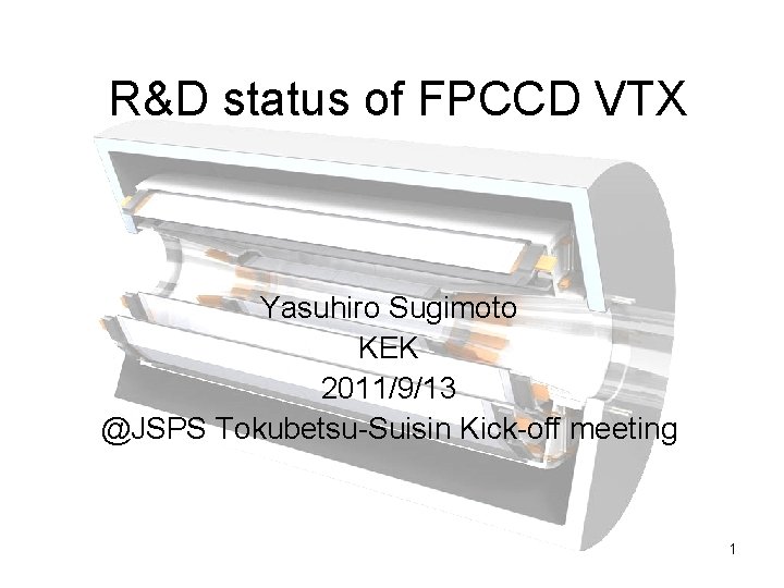
R&D status of FPCCD VTX Yasuhiro Sugimoto KEK 2011/9/13 @JSPS Tokubetsu-Suisin Kick-off meeting 1

Outline • Introduction – Vertex detector for ILC – R&D goals • FPCCD sensor R&D – Prototypes – CTI simulation • ASIC R&D Kato-san’s talk • Engineering R&D – Wafer thinning – CO 2 cooling system – Engineering common design 2

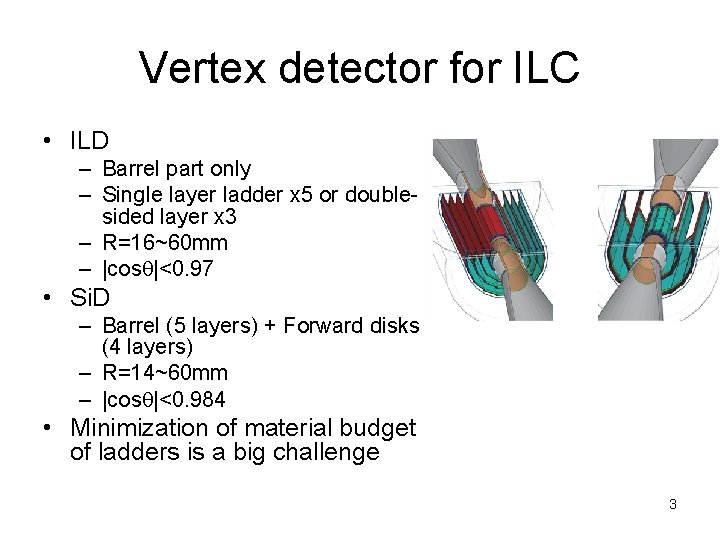
Vertex detector for ILC • ILD – Barrel part only – Single layer ladder x 5 or doublesided layer x 3 – R=16~60 mm – |cosq|<0. 97 • Si. D – Barrel (5 layers) + Forward disks (4 layers) – R=14~60 mm – |cosq|<0. 984 • Minimization of material budget of ladders is a big challenge 3

Performance goal of ILC VTX • Impact parameter resolution: s. IP<5 10/(pbsin 3/2 q ) mm – Measurement accuracy < 3 mm – Material budget < 0. 1%X 0/layer • Tolerance against beam background – Pixel occupancy < few% – Radiation immunity: 1 x 10¹² e/cm 2/y • Tolerance against RF noise – RF noise is induced by bunched beam – It was a serious problem at SLD • There are many sensor options proposed to solve these challenges • One possible solution for these issues:FPCCD – Fine Pixel CCD: ~5 mm pixel – Read out in 200 ms between beam trains 4

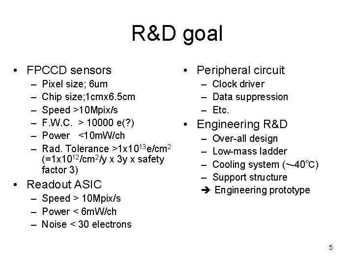
R&D goal • FPCCD sensors – – – Pixel size; 6 um Chip size; 1 cmx 6. 5 cm Speed >10 Mpix/s F. W. C. > 10000 e(? ) Power <10 m. W/ch Rad. Tolerance >1 x 10¹³ e/cm 2 (=1 x 10¹²/cm 2/y x 3 y x safety factor 3) • Readout ASIC – Speed > 10 Mpix/s – Power < 6 m. W/ch – Noise < 30 electrons • Peripheral circuit – Clock driver – Data suppression – Etc. • Engineering R&D – Over-all design – Low-mass ladder – Cooling system (~-40℃) – Support structure Engineering prototype 5

FPCCD sensor R&D 6

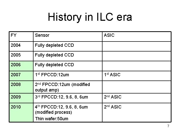
History in ILC era FY Sensor ASIC 2004 Fully depleted CCD 2005 Fully depleted CCD 2006 Fully depleted CCD 2007 1 st FPCCD: 12 um 2008 2 nd FPCCD: 12 um (modified output amp) 2009 3 rd FPCCD: 12, 9. 6, 8, 6 um 2 nd ASIC 2010 4 th FPCCD: 12, 9. 6, 8, 6 um (modified process) Thin wafer: 50 um 2 nd ASIC 1 st ASIC 7

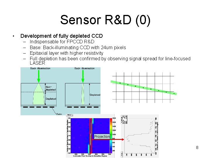
Sensor R&D (0) • Development of fully depleted CCD – – Indispensable for FPCCD R&D Base: Back-illuminating CCD with 24 um pixels Epitaxial layer with higher resistivity Full depletion has been confirmed by observing signal spread for line-focused LASER Projection 8

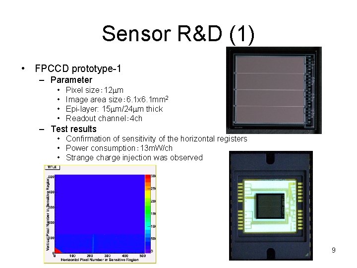
Sensor R&D (1) • FPCCD prototype-1 – Parameter • • Pixel size: 12 mm Image area size: 6. 1 x 6. 1 mm 2 Epi-layer: 15 mm/24 mm thick Readout channel: 4 ch – Test results • Confirmation of sensitivity of the horizontal registers • Power consumption: 13 m. W/ch • Strange charge injection was observed 9

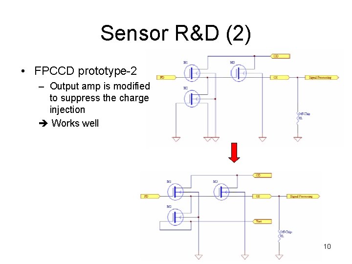
Sensor R&D (2) • FPCCD prototype-2 – Output amp is modified to suppress the charge injection Works well 10

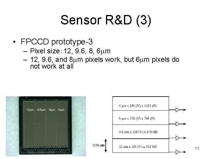
Sensor R&D (3) • FPCCD prototype-3 – Pixel size: 12, 9. 6, 8, 6 mm – 12, 9. 6, and 8 mm pixels work, but 6 mm pixels do not work at all 12 mm 9. 6 mm 8 mm 6 mm 11

Sensor R&D (4) • FPCCD prototype-4 – Same parameters as prototype-3 – Improvement of potential profile based on device simulator – x 2 improvement of the depth of the potential well is expected – 6 mm pixel works, but not properly • FPCCD prototype-5 (to be delivered FY 2012) – First large size (~1 cmx 6 cm) prototype – Horizontal shift register for 6 mm pixel has a size of 6 mmx 12 mm to improve full-well capacity and to decrease resistance of gate line – Multiple wire for gate: Many bonding pads along the longer side of the chip 12

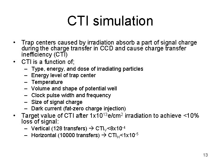
CTI simulation • Trap centers caused by irradiation absorb a part of signal charge during the charge transfer in CCD and cause charge transfer inefficiency (CTI) • CTI is a function of; – – – – Type, energy, and dose of irradiating particles Energy level of trap center Temperature Volume and shape of potential well Clock pulse width and frequency Size of signal charge Dark current (fat-zero charge injection) • Target value of CTI after 1 x 10¹³ e/cm 2 irradiation to achieve <10% loss of signal: – Vertical (128 transfers) CTIV<8 x 10 -4 – Horizontal (10000 transfers) CTIH<1 x 10 -5 13

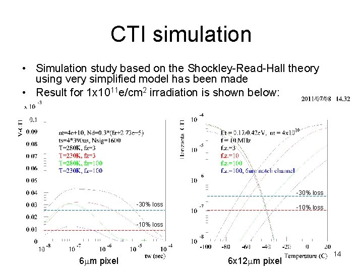
CTI simulation • Simulation study based on the Shockley-Read-Hall theory using very simplified model has been made • Result for 1 x 10¹¹ e/cm 2 irradiation is shown below: -30% loss -10% loss 6 mm pixel 6 x 12 mm pixel 14

CTI simulation • Satisfactory low vertical CTI would be achieved at ~-40 degrees if wide (>10 ms) clock pulse is used and small amount of fat-zero charge is injected • Horizontal CTI gets its minimum at ~-40 degrees, but it is marginal to achieve the required value • In order to achieve the target value of H-CTI; – Width of the charge transfer channel should be less than 6 mm rather than 12 mm Notch channel – Large amount of fat-zero charge should be injected 15

Engineering R&D 16

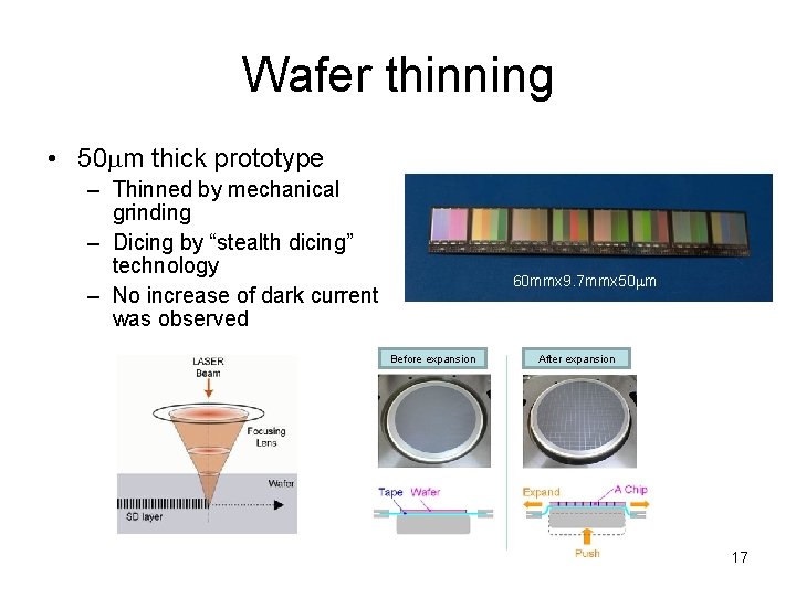
Wafer thinning • 50 mm thick prototype – Thinned by mechanical grinding – Dicing by “stealth dicing” technology – No increase of dark current was observed 60 mmx 9. 7 mmx 50 mm Before expansion After expansion 17

CO 2 cooling system • FPCCD will be operated at low temperature (-40 degree) to minimize CTI • Power consumption – Inside cryostat: 4224 readout channel ~100 W • Cooling with cold air (nitrogen) flow would not be enough • Cooling system using 2 -phase CO 2 is a very attractive alternative because of its large cooling capacity (~300 J/g) • Cooling tube is attached to VTX end-plate and heat produced by CCD output amp and ASIC is removed by conduction through CFRP ladder (simulation study for thermal design is necessary) • Return line of CO 2 will be used to cool the electronics outside the cryostat (~200 W/side) • Inner support tube should be air-tight and filled with dry air/nitrogen in order to prevent condensation on the CO 2 tube 18

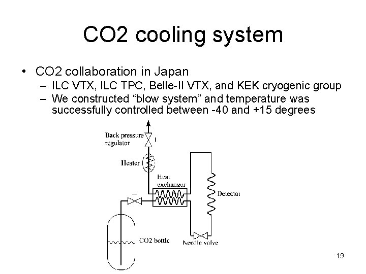
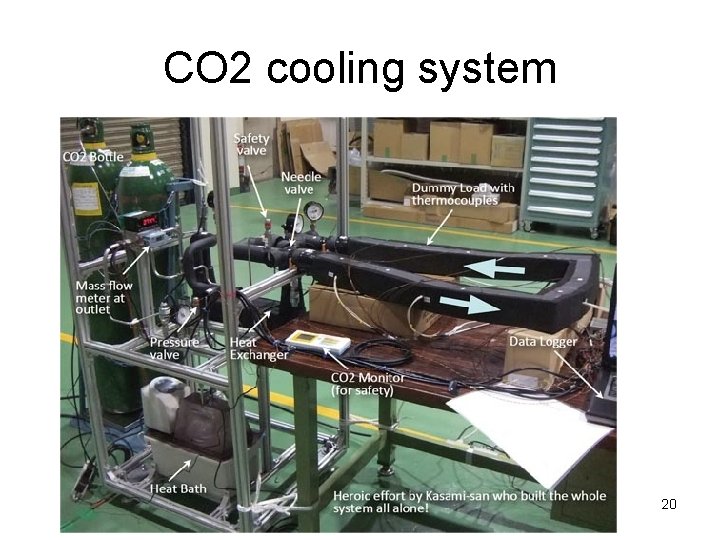
CO 2 cooling system • CO 2 collaboration in Japan – ILC VTX, ILC TPC, Belle-II VTX, and KEK cryogenic group – We constructed “blow system” and temperature was successfully controlled between -40 and +15 degrees 19

CO 2 cooling system 20

Common engineering design • A tentative engineering design of VTX which is common to all sensor options have been made to be used in ILD detector simulation (MOKKA) for DBD • GEANT 4 simulation is common to all sensor options (50 mm thick Si), and the study of different sensor option can be done at digitization phase • The design is based on SLD VTX • Double sided ladder option is assumed • Compared with old model (ILD 00), material budget in forward region is increased • Implementation into MOKKA will be done by Gabriel Musat and Georgios Gerasimos Voutsinas 21

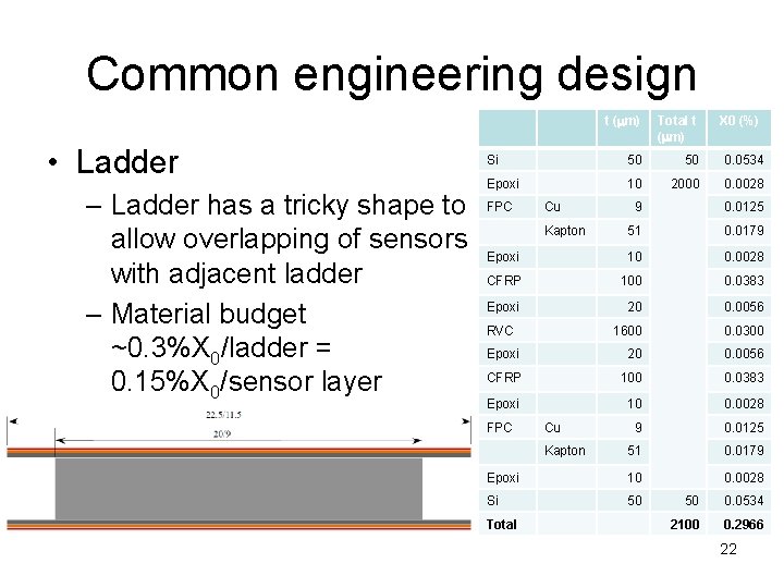
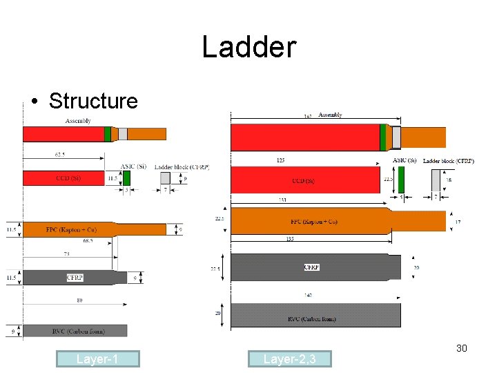
Common engineering design • Ladder – Ladder has a tricky shape to allow overlapping of sensors with adjacent ladder – Material budget ~0. 3%X 0/ladder = 0. 15%X 0/sensor layer t (mm) Total t (mm) Si 50 50 0. 0534 Epoxi 10 2000 0. 0028 FPC Cu X 0 (%) 9 0. 0125 51 0. 0179 Epoxi 10 0. 0028 CFRP 100 0. 0383 Epoxi 20 0. 0056 1600 0. 0300 Epoxi 20 0. 0056 CFRP 100 0. 0383 Epoxi 10 0. 0028 9 0. 0125 51 0. 0179 Epoxi 10 0. 0028 Si 50 Kapton RVC FPC Cu Kapton Total 50 0. 0534 2100 0. 2966 22

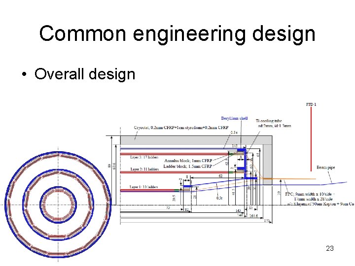
Common engineering design • Overall design 23

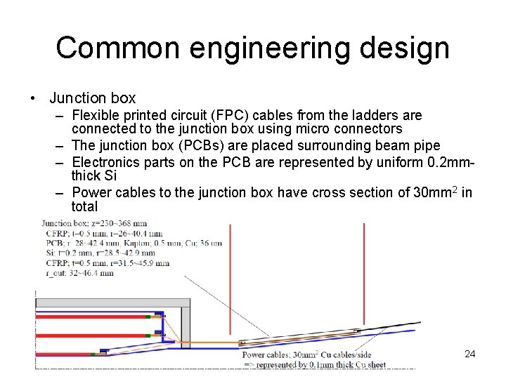
Common engineering design • Junction box – Flexible printed circuit (FPC) cables from the ladders are connected to the junction box using micro connectors – The junction box (PCBs) are placed surrounding beam pipe – Electronics parts on the PCB are represented by uniform 0. 2 mmthick Si – Power cables to the junction box have cross section of 30 mm 2 in total 24

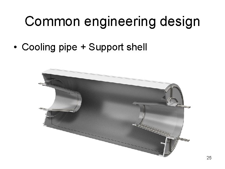
Common engineering design • Cooling pipe + Support shell 25

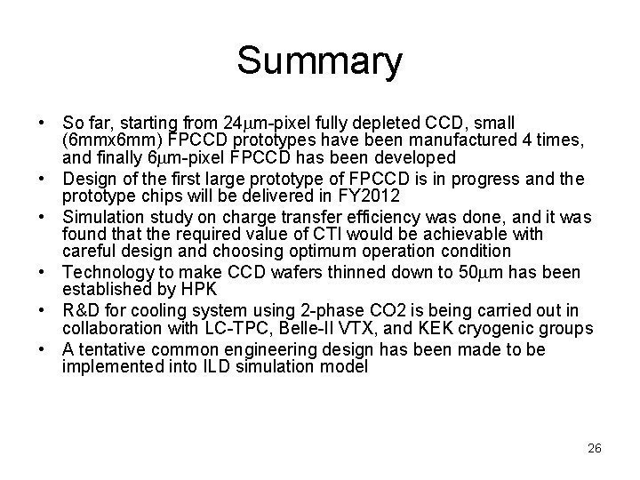
Summary • So far, starting from 24 mm-pixel fully depleted CCD, small (6 mmx 6 mm) FPCCD prototypes have been manufactured 4 times, and finally 6 mm-pixel FPCCD has been developed • Design of the first large prototype of FPCCD is in progress and the prototype chips will be delivered in FY 2012 • Simulation study on charge transfer efficiency was done, and it was found that the required value of CTI would be achievable with careful design and choosing optimum operation condition • Technology to make CCD wafers thinned down to 50 mm has been established by HPK • R&D for cooling system using 2 -phase CO 2 is being carried out in collaboration with LC-TPC, Belle-II VTX, and KEK cryogenic groups • A tentative common engineering design has been made to be implemented into ILD simulation model 26

Backup slides 27

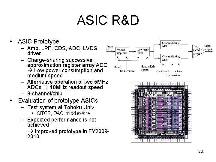
ASIC R&D • ASIC Prototype – Amp, LPF, CDS, ADC, LVDS driver – Charge-sharing successive approximation register array ADC Low power consumption and medium speed – Alternative operation of two 5 MHz ADCs 10 MHz readout speed – 8 -channel/chip • Evaluation of prototype ASICs – Test system at Tohoku Univ. • Si. TCP, DAQ-middleware – Expected performance is not achieved Improved prototype in FY 20092010 28

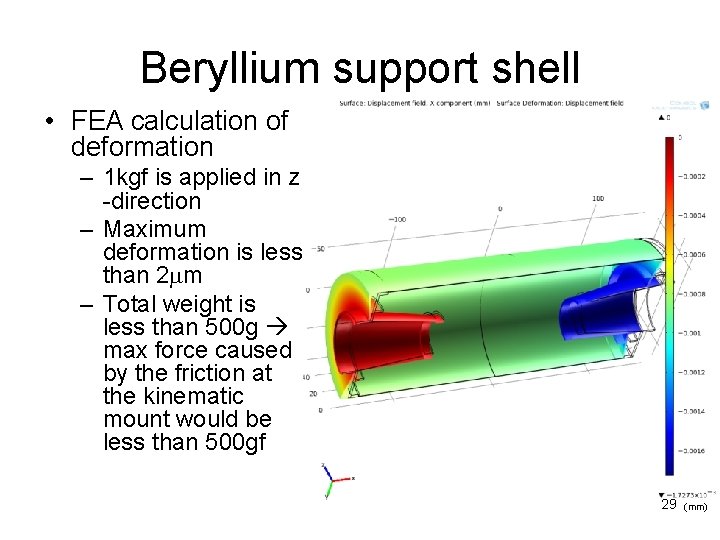
Beryllium support shell • FEA calculation of deformation – 1 kgf is applied in z -direction – Maximum deformation is less than 2 mm – Total weight is less than 500 g max force caused by the friction at the kinematic mount would be less than 500 gf 29 (mm)

Ladder • Structure Layer-1 Layer-2, 3 30

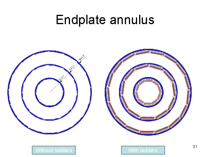
Endplate annulus Without ladders With ladders 31

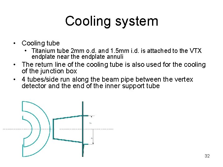
Cooling system • Cooling tube • Titanium tube 2 mm o. d. and 1. 5 mm i. d. is attached to the VTX endplate near the endplate annuli • The return line of the cooling tube is also used for the cooling of the junction box • 4 tubes/side run along the beam pipe between the vertex detector and the end of the inner support tube 32