RD of FPCCD Yasuhiro Sugimoto KEK 25 Nov

- Slides: 20

R&D of FPCCD Yasuhiro Sugimoto KEK 25 Nov. 2008 1

Collaboration l KEK l l JAXA/ISAS l l H. Ikeda Tohoku University l l A. Miyamoto, K. Nakayoshi, Y. Sugimoto K. Itagaki, T. Nagamine, Y. Takubo, H. Yamamoto Tohoku Gakuin University l K. Abe 2

Basic concept l l FPCCD (Fine Pixel CCD) is one of the candidate sensor technologies for ILC vertex detector ILC “pair background” at small R l ~5000 hits/cm 2/train with B=3 T and R=20 mm l Pixel occupancy ~10% for 25 mm pixel (several pixels are fired for one track hit) l In order to keep the occupancy small (<1%), l l read out 20 times per train (1 ms), or 20 times finer pixel Fine Pixel CCD (FPCCD) is necessary 3

Advantages of FPCCD VTX l l l l Completely free from beam-induced RF noise (EMI) Excellent spatial resolution of sx~1. 4 mm even with digital readout Excellent two-track separation capability because of fine pixels and fully depleted epitaxial layer Capability of low-energy pair-background rejection by making use of hit-cluster shape Simple structure which enables large wafer size with high yield rate No heat source in the image area No need for very high readout speed 4

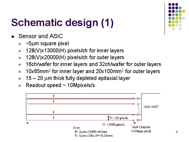
Schematic design (1) l Sensor and ASIC l l l l ~5 mm square pixel 128(V)x 13000(H) pixels/ch for inner layers 128(V)x 20000(H) pixels/ch for outer layers 16 ch/wafer for inner layers and 32 ch/wafer for outer layers 10 x 65 mm 2 for inner layer and 20 x 100 mm 2 for outer layers 15 – 20 mm thick fully depleted epitaxial layer Readout speed ~ 10 Mpixels/s 5

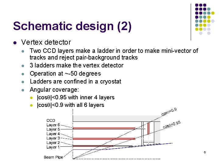
Schematic design (2) l Vertex detector l l l Two CCD layers make a ladder in order to make mini-vector of tracks and reject pair-background tracks 3 ladders make the vertex detector Operation at ~-50 degrees Ladders are confined in a cryostat Angular coverage: l l |cosq|<0. 95 with inner 4 layers |cosq|<0. 9 with all 6 layers 6

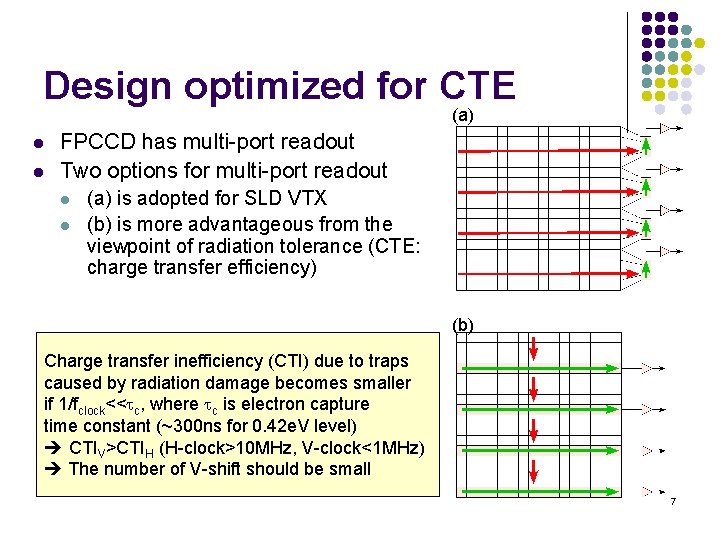
Design optimized for CTE (a) l l FPCCD has multi-port readout Two options for multi-port readout l l (a) is adopted for SLD VTX (b) is more advantageous from the viewpoint of radiation tolerance (CTE: charge transfer efficiency) (b) Charge transfer inefficiency (CTI) due to traps caused by radiation damage becomes smaller if 1/fclock<<tc, where tc is electron capture time constant (~300 ns for 0. 42 e. V level) CTIV>CTIH (H-clock>10 MHz, V-clock<1 MHz) The number of V-shift should be small 7

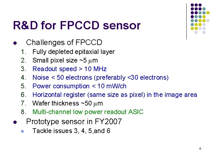
R&D for FPCCD sensor Challenges of FPCCD l 1. 2. 3. 4. 5. 6. 7. 8. Fully depleted epitaxial layer Small pixel size ~5 mm Readout speed > 10 MHz Noise < 50 electrons (preferably <30 electrons) Power consumption < 10 m. W/ch Horizontal register (same size as pixel) in the image area Wafer thickness ~50 mm Multi-channel low power readout ASIC Prototype sensor in FY 2007 l l Tackle issues 3, 4, 5, and 6 8

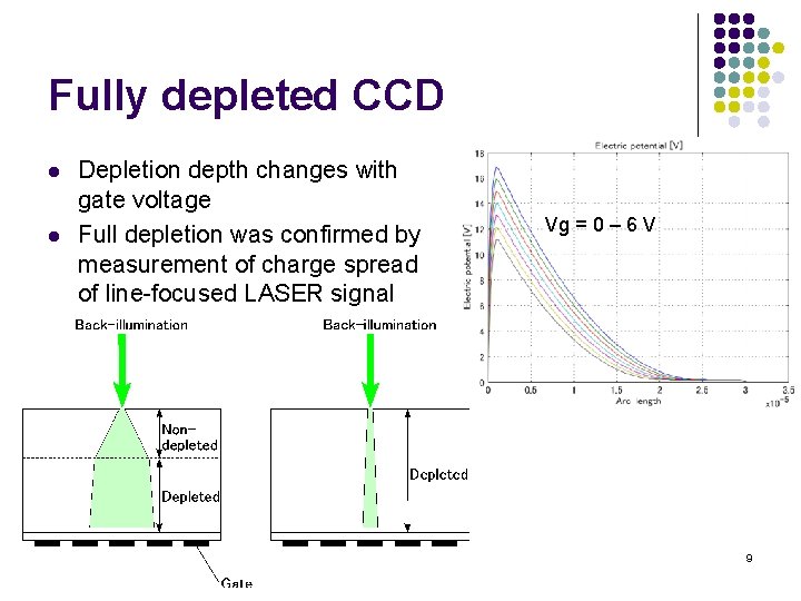
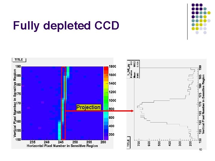
Fully depleted CCD l l Depletion depth changes with gate voltage Full depletion was confirmed by measurement of charge spread of line-focused LASER signal Vg = 0 – 6 V 9

Fully depleted CCD Projection 10

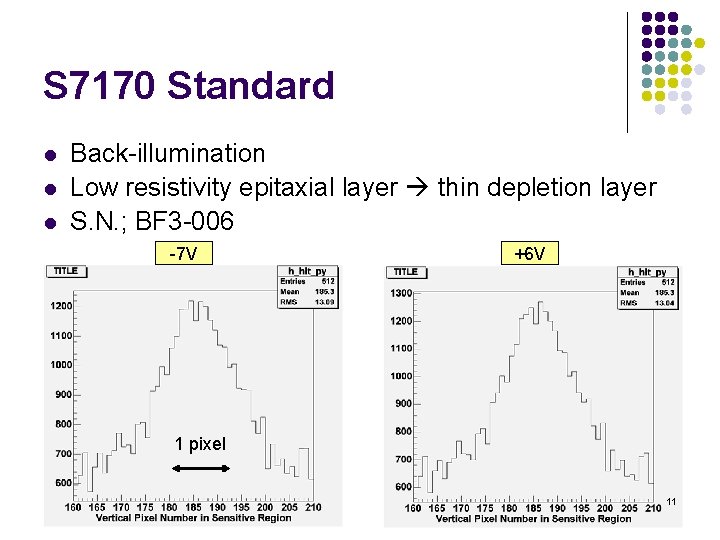
S 7170 Standard l l l Back-illumination Low resistivity epitaxial layer thin depletion layer S. N. ; BF 3 -006 -7 V +6 V 1 pixel 11

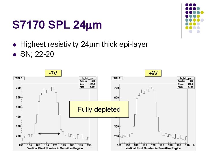
S 7170 SPL 24 mm l l Highest resistivity 24 mm thick epi-layer SN; 22 -20 -7 V +6 V Fully depleted 12

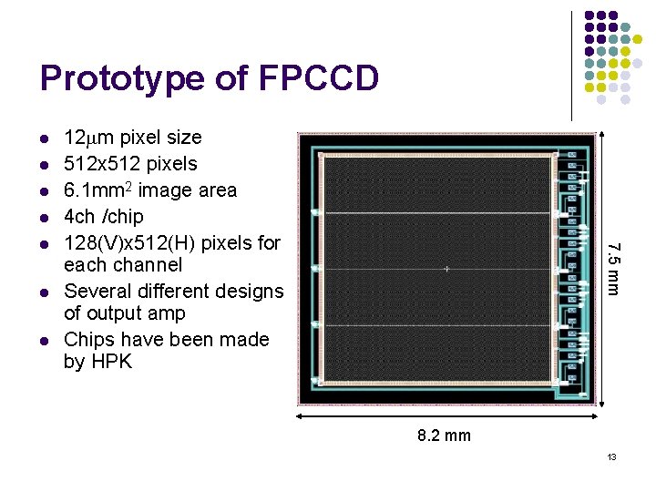
Prototype of FPCCD l l l 7. 5 mm l 12 mm pixel size 512 x 512 pixels 6. 1 mm 2 image area 4 ch /chip 128(V)x 512(H) pixels for each channel Several different designs of output amp Chips have been made by HPK 8. 2 mm 13

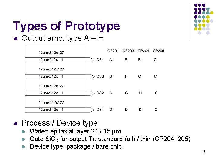
Types of Prototype l Output amp: type A – H l Process / Device type l l l Wafer: epitaxial layer 24 / 15 mm Gate Si. O 2 for output Tr: standard (all) / thin (CP 204, 205) Device type: package / bare chip 14

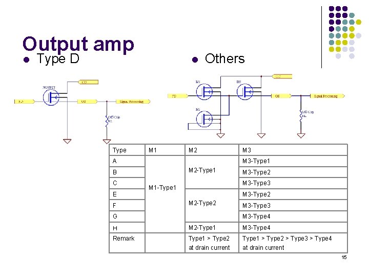
Output amp l Type D Type l M 1 Others M 2 A M 3 -Type 1 M 2 -Type 1 B C E F M 3 -Type 2 M 3 -Type 3 M 1 -Type 1 M 3 -Type 2 M 2 -Type 2 G M 3 -Type 3 M 3 -Type 4 H M 2 -Type 1 M 3 -Type 4 Remark Type 1 > Type 2 at drain current Type 1 > Type 2 > Type 3 > Type 4 at drain current 15

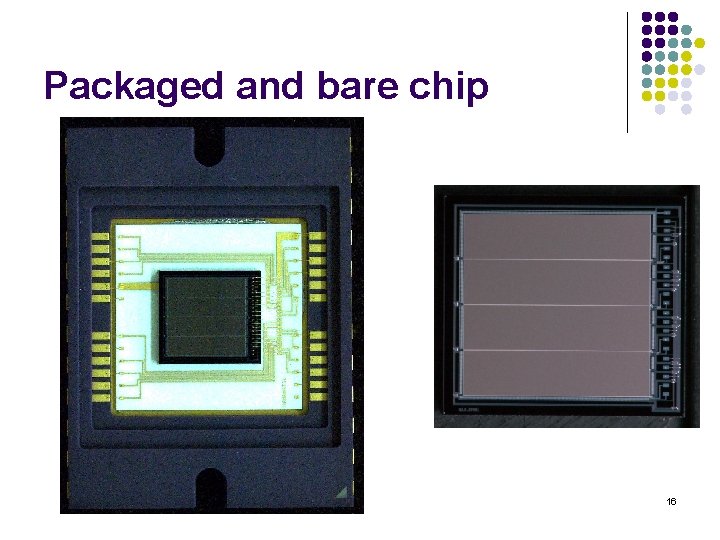
Packaged and bare chip 16

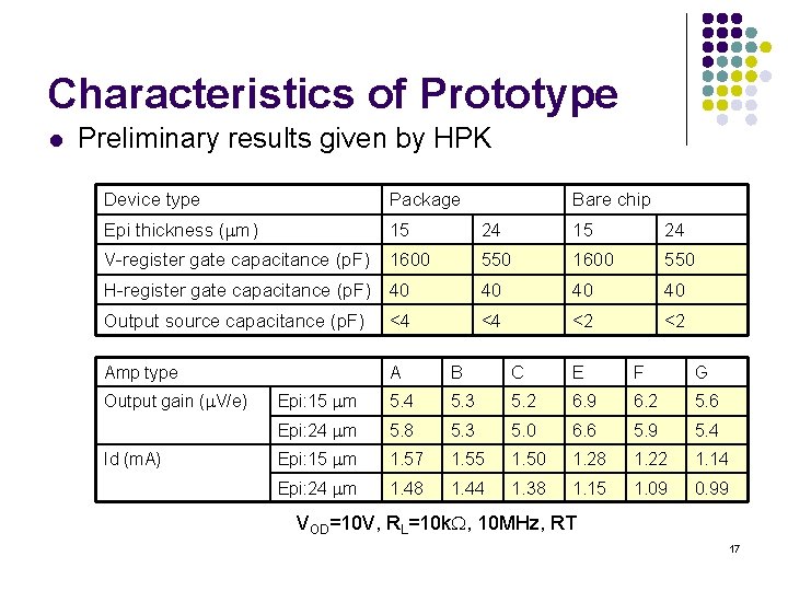
Characteristics of Prototype l Preliminary results given by HPK Device type Package Epi thickness (mm) 15 24 V-register gate capacitance (p. F) 1600 550 H-register gate capacitance (p. F) 40 40 Output source capacitance (p. F) <4 <4 <2 <2 Amp type A B C E F G Epi: 15 mm 5. 4 5. 3 5. 2 6. 9 6. 2 5. 6 Epi: 24 mm 5. 8 5. 3 5. 0 6. 6 5. 9 5. 4 Epi: 15 mm 1. 57 1. 55 1. 50 1. 28 1. 22 1. 14 Epi: 24 mm 1. 48 1. 44 1. 38 1. 15 1. 09 0. 99 Output gain (m. V/e) Id (m. A) Bare chip VOD=10 V, RL=10 k. W, 10 MHz, RT 17

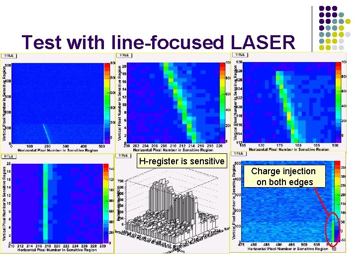
Test with line-focused LASER H-register is sensitive Charge injection on both edges 18

Plan for FY 2008 prototype l l Same pixel (12 mm) and chip size Larger full-well capacity No charge injection Double Al layers to reduce R of H-register 19

Summary and outlook l l l R&D of FPCCD is being carried out for ILC VTX application Fully depleted epitaxial layer – one of the key issues of FPCCD – is achieved with high resistivity 24 mm-thick epitaxial layer The first prototype FPCCDs have been made by HPK l l l l Detailed study on the prototype FPCCDs has started l l Pixel size: 12 mm H-register same size as pixels 4 ch/chip Several types of output circuit Two different epitaxial layer thickness (15 / 24 mm) Two different gate oxide thickness for output transistors H-register is sensitive Charge injection is seen on both edges of the chip Improved prototype is planned in FY 2008 Full size (10 x 65 mm) prototype by 2012, if possible 20