RD status of FPCCD VTX Yasuhiro Sugimoto KEK
- Slides: 12

R&D status of FPCCD VTX Yasuhiro Sugimoto KEK 17 Nov. 2008 @LCWS 2008 1

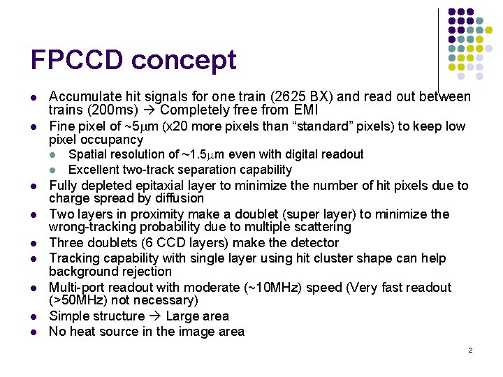
FPCCD concept l Accumulate hit signals for one train (2625 BX) and read out between trains (200 ms) Completely free from EMI l Fine pixel of ~5 mm (x 20 more pixels than “standard” pixels) to keep low pixel occupancy l l l l l Spatial resolution of ~1. 5 mm even with digital readout Excellent two-track separation capability Fully depleted epitaxial layer to minimize the number of hit pixels due to charge spread by diffusion Two layers in proximity make a doublet (super layer) to minimize the wrong-tracking probability due to multiple scattering Three doublets (6 CCD layers) make the detector Tracking capability with single layer using hit cluster shape can help background rejection Multi-port readout with moderate (~10 MHz) speed (Very fast readout (>50 MHz) not necessary) Simple structure Large area No heat source in the image area 2

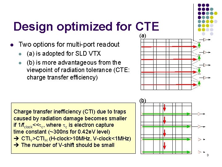
Design optimized for CTE (a) l Two options for multi-port readout l l (a) is adopted for SLD VTX (b) is more advantageous from the viewpoint of radiation tolerance (CTE: charge transfer efficiency) (b) Charge transfer inefficiency (CTI) due to traps caused by radiation damage becomes smaller if 1/fclock<<tc, where tc is electron capture time constant (~300 ns for 0. 42 e. V level) CTIV>CTIH (H-clock>10 MHz, V-clock<1 MHz) The number of V-shift should be small 3

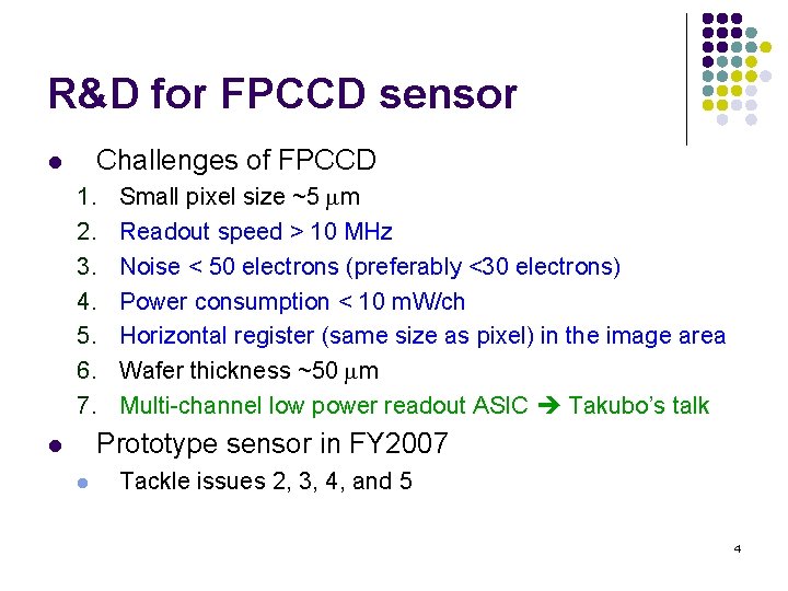
R&D for FPCCD sensor Challenges of FPCCD l 1. 2. 3. 4. 5. 6. 7. Small pixel size ~5 mm Readout speed > 10 MHz Noise < 50 electrons (preferably <30 electrons) Power consumption < 10 m. W/ch Horizontal register (same size as pixel) in the image area Wafer thickness ~50 mm Multi-channel low power readout ASIC Takubo’s talk Prototype sensor in FY 2007 l l Tackle issues 2, 3, 4, and 5 4

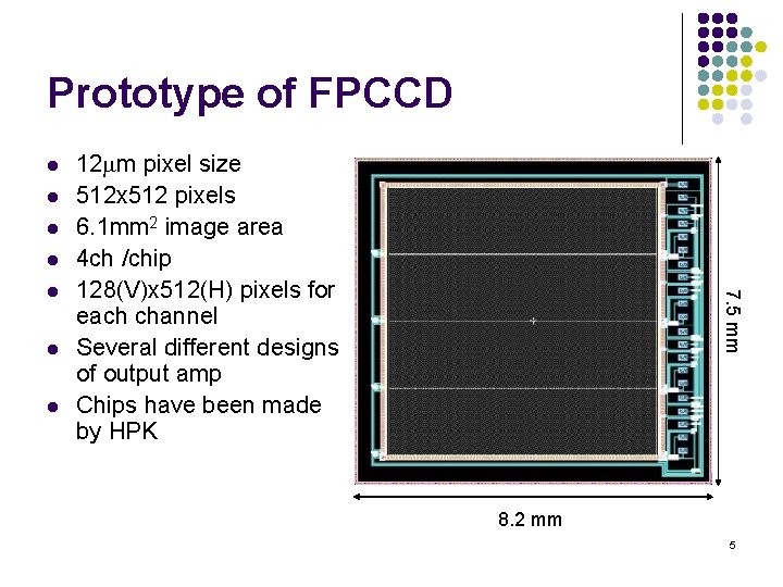
Prototype of FPCCD l l l 7. 5 mm l 12 mm pixel size 512 x 512 pixels 6. 1 mm 2 image area 4 ch /chip 128(V)x 512(H) pixels for each channel Several different designs of output amp Chips have been made by HPK 8. 2 mm 5

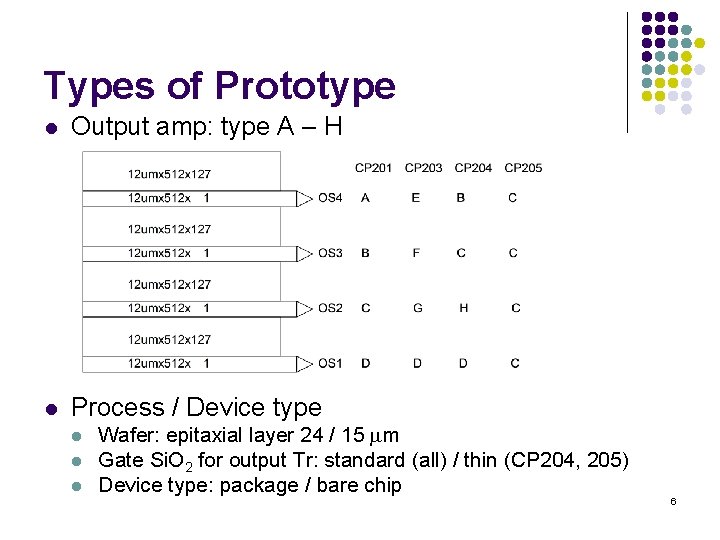
Types of Prototype l Output amp: type A – H l Process / Device type l l l Wafer: epitaxial layer 24 / 15 mm Gate Si. O 2 for output Tr: standard (all) / thin (CP 204, 205) Device type: package / bare chip 6

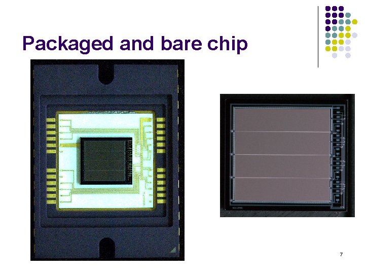
Packaged and bare chip 7

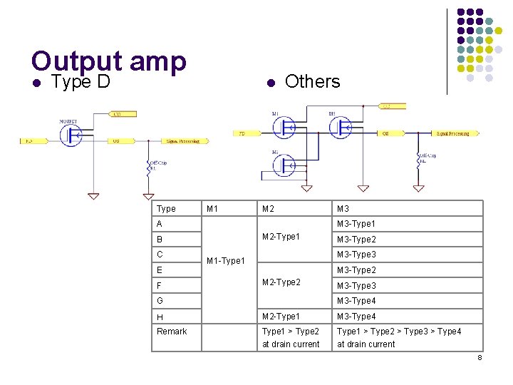
Output amp l Type D Type l M 1 Others M 2 A M 3 -Type 1 M 2 -Type 1 B C E F M 3 -Type 2 M 3 -Type 3 M 1 -Type 1 M 3 -Type 2 M 2 -Type 2 G M 3 -Type 3 M 3 -Type 4 H M 2 -Type 1 M 3 -Type 4 Remark Type 1 > Type 2 at drain current Type 1 > Type 2 > Type 3 > Type 4 at drain current 8

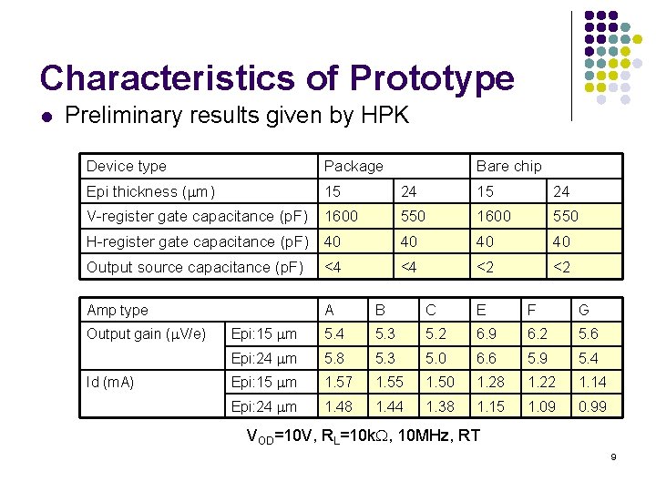
Characteristics of Prototype l Preliminary results given by HPK Device type Package Epi thickness (mm) 15 24 V-register gate capacitance (p. F) 1600 550 H-register gate capacitance (p. F) 40 40 Output source capacitance (p. F) <4 <4 <2 <2 Amp type A B C E F G Epi: 15 mm 5. 4 5. 3 5. 2 6. 9 6. 2 5. 6 Epi: 24 mm 5. 8 5. 3 5. 0 6. 6 5. 9 5. 4 Epi: 15 mm 1. 57 1. 55 1. 50 1. 28 1. 22 1. 14 Epi: 24 mm 1. 48 1. 44 1. 38 1. 15 1. 09 0. 99 Output gain (m. V/e) Id (m. A) Bare chip VOD=10 V, RL=10 k. W, 10 MHz, RT 9

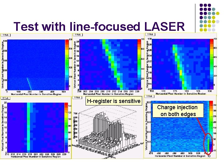
Test with line-focused LASER H-register is sensitive Charge injection on both edges 10

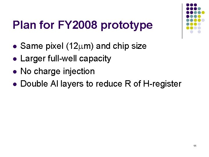
Plan for FY 2008 prototype l l Same pixel (12 mm) and chip size Larger full-well capacity No charge injection Double Al layers to reduce R of H-register 11

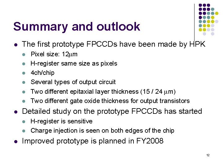
Summary and outlook l The first prototype FPCCDs have been made by HPK l l l l Detailed study on the prototype FPCCDs has started l l l Pixel size: 12 mm H-register same size as pixels 4 ch/chip Several types of output circuit Two different epitaxial layer thickness (15 / 24 mm) Two different gate oxide thickness for output transistors H-register is sensitive Charge injection is seen on both edges of the chip Improved prototype is planned in FY 2008 12