FPCCD VTX Overview Yasuhiro Sugimoto KEK 20121220 JSPS

- Slides: 18

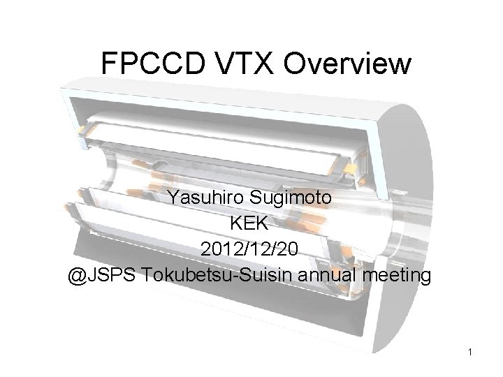
FPCCD VTX Overview Yasuhiro Sugimoto KEK 2012/12/20 @JSPS Tokubetsu-Suisin annual meeting 1

Outline • • FPCCD VTX for ILD FPCCD sensor R&D CO 2 cooling for VTX FY 2013 plan 2

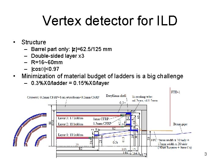
Vertex detector for ILD • Structure – – Barrel part only: |z|=62. 5/125 mm Double-sided layer x 3 R=16~60 mm |cosq|<0. 97 • Minimization of material budget of ladders is a big challenge – 0. 3%X 0/ladder = 0. 15%X 0/layer 3

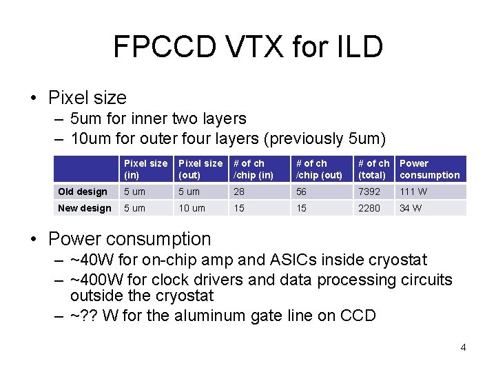
FPCCD VTX for ILD • Pixel size – 5 um for inner two layers – 10 um for outer four layers (previously 5 um) Pixel size (in) Pixel size (out) # of ch /chip (in) # of ch /chip (out) # of ch (total) Power consumption Old design 5 um 28 56 7392 111 W New design 5 um 10 um 15 15 2280 34 W • Power consumption – ~40 W for on-chip amp and ASICs inside cryostat – ~400 W for clock drivers and data processing circuits outside the cryostat – ~? ? W for the aluminum gate line on CCD 4

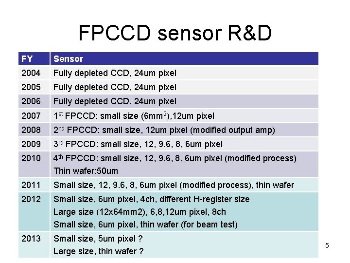
FPCCD sensor R&D FY Sensor 2004 Fully depleted CCD, 24 um pixel 2005 Fully depleted CCD, 24 um pixel 2006 Fully depleted CCD, 24 um pixel 2007 1 st FPCCD: small size (6 mm 2), 12 um pixel 2008 2 nd FPCCD: small size, 12 um pixel (modified output amp) 2009 3 rd FPCCD: small size, 12, 9. 6, 8, 6 um pixel 2010 4 th FPCCD: small size, 12, 9. 6, 8, 6 um pixel (modified process) Thin wafer: 50 um 2011 Small size, 12, 9. 6, 8, 6 um pixel (modified process), thin wafer 2012 Small size, 6 um pixel, 4 ch, different H-register size Large size (12 x 64 mm 2), 6, 8, 12 um pixel, 8 ch Small size, 6 um pixel, thin wafer (for beam test) 2013 Small size, 5 um pixel ? Large size, thin wafer ? 5

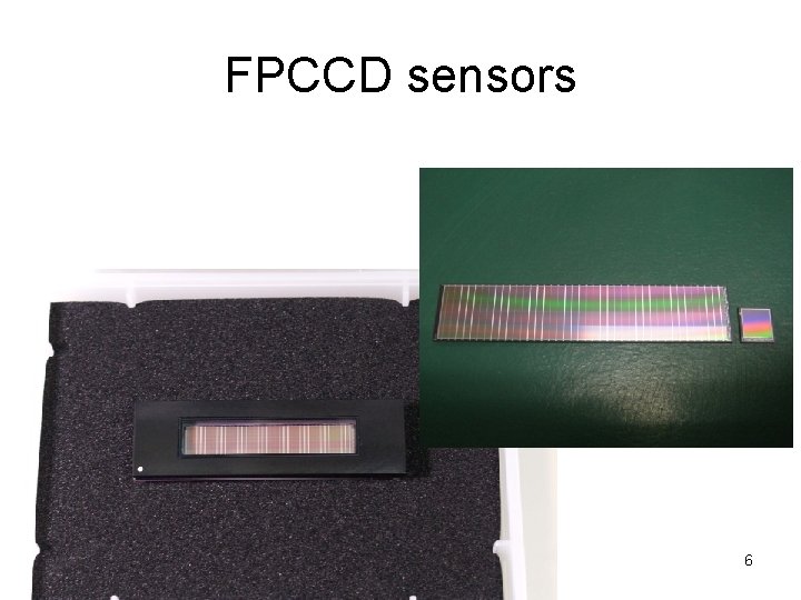
FPCCD sensors 6

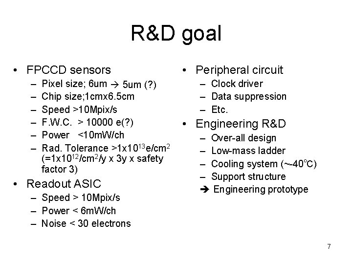
R&D goal • FPCCD sensors – – – Pixel size; 6 um 5 um (? ) Chip size; 1 cmx 6. 5 cm Speed >10 Mpix/s F. W. C. > 10000 e(? ) Power <10 m. W/ch Rad. Tolerance >1 x 10¹³ e/cm 2 (=1 x 10¹²/cm 2/y x 3 y x safety factor 3) • Readout ASIC – Speed > 10 Mpix/s – Power < 6 m. W/ch – Noise < 30 electrons • Peripheral circuit – Clock driver – Data suppression – Etc. • Engineering R&D – Over-all design – Low-mass ladder – Cooling system (~-40℃) – Support structure Engineering prototype 7

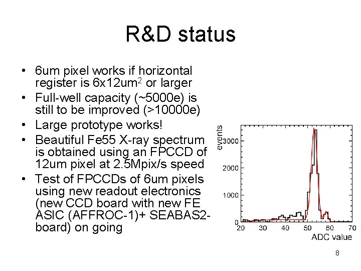
R&D status • 6 um pixel works if horizontal register is 6 x 12 um 2 or larger • Full-well capacity (~5000 e) is still to be improved (>10000 e) • Large prototype works! • Beautiful Fe 55 X-ray spectrum is obtained using an FPCCD of 12 um pixel at 2. 5 Mpix/s speed • Test of FPCCDs of 6 um pixels using new readout electronics (new CCD board with new FE ASIC (AFFROC-1)+ SEABAS 2 board) on going 8

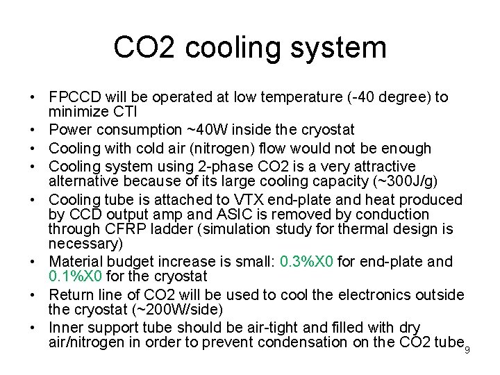
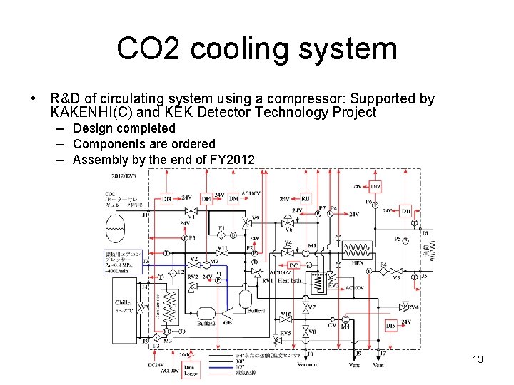
CO 2 cooling system • FPCCD will be operated at low temperature (-40 degree) to minimize CTI • Power consumption ~40 W inside the cryostat • Cooling with cold air (nitrogen) flow would not be enough • Cooling system using 2 -phase CO 2 is a very attractive alternative because of its large cooling capacity (~300 J/g) • Cooling tube is attached to VTX end-plate and heat produced by CCD output amp and ASIC is removed by conduction through CFRP ladder (simulation study for thermal design is necessary) • Material budget increase is small: 0. 3%X 0 for end-plate and 0. 1%X 0 for the cryostat • Return line of CO 2 will be used to cool the electronics outside the cryostat (~200 W/side) • Inner support tube should be air-tight and filled with dry air/nitrogen in order to prevent condensation on the CO 2 tube 9

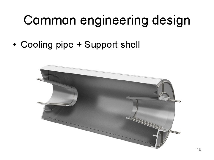
Common engineering design • Cooling pipe + Support shell 10

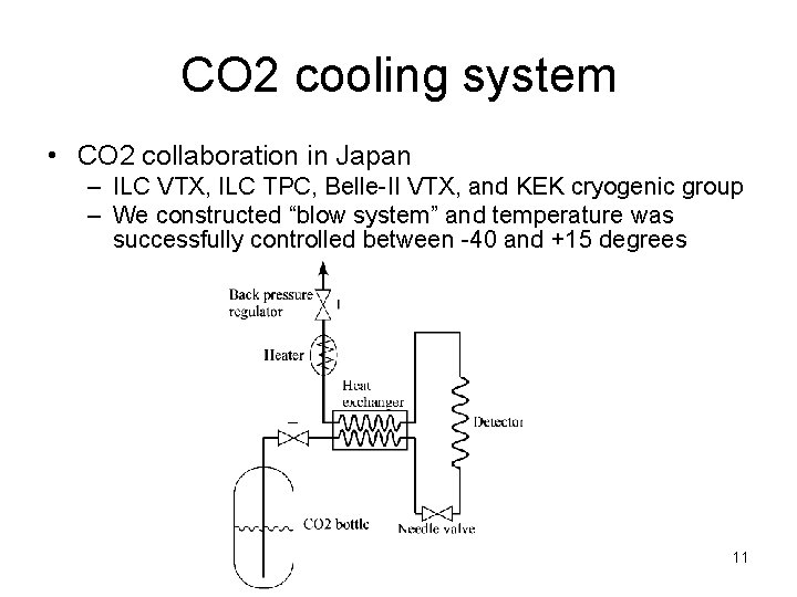
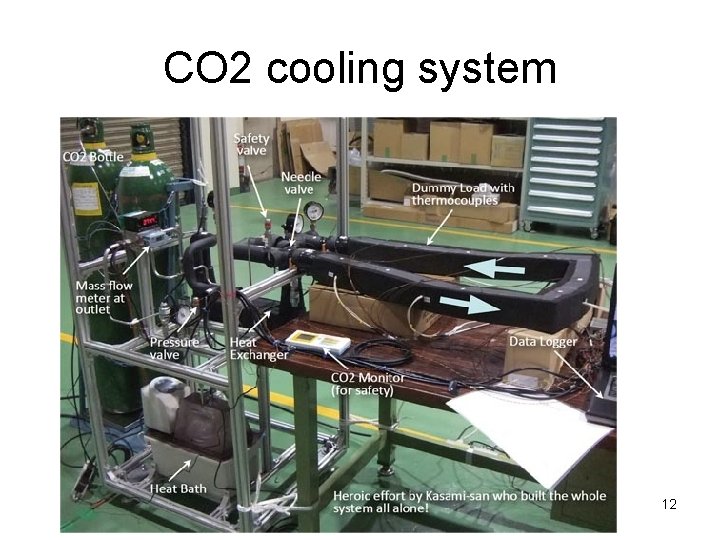
CO 2 cooling system • CO 2 collaboration in Japan – ILC VTX, ILC TPC, Belle-II VTX, and KEK cryogenic group – We constructed “blow system” and temperature was successfully controlled between -40 and +15 degrees 11

CO 2 cooling system 12

CO 2 cooling system • R&D of circulating system using a compressor: Supported by KAKENHI(C) and KEK Detector Technology Project – Design completed – Components are ordered – Assembly by the end of FY 2012 13

FY 2013 plan • Beam test – Demonstrate spatial resolution – Test beam at JPARC (1 Ge. V) • Neutron damage test – Few tens of Me. V/c neutron beam is available at CYRIC cyclotron in Tohoku University – FPCCD neutron damage test in FY 2013~2014 • FPCCD Prototypes – Large thin wafer (? ) – Small 5 um pixel chip (? ) • 2 nd AFFROC prototype, if necessary • Bare chip test – Fabricate a test board for bare chips before ladder R&D 14

Backup slides 15

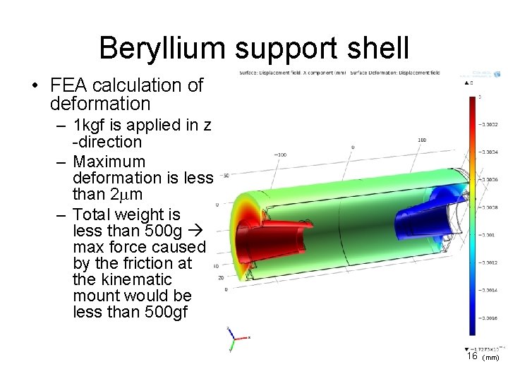
Beryllium support shell • FEA calculation of deformation – 1 kgf is applied in z -direction – Maximum deformation is less than 2 mm – Total weight is less than 500 g max force caused by the friction at the kinematic mount would be less than 500 gf 16 (mm)

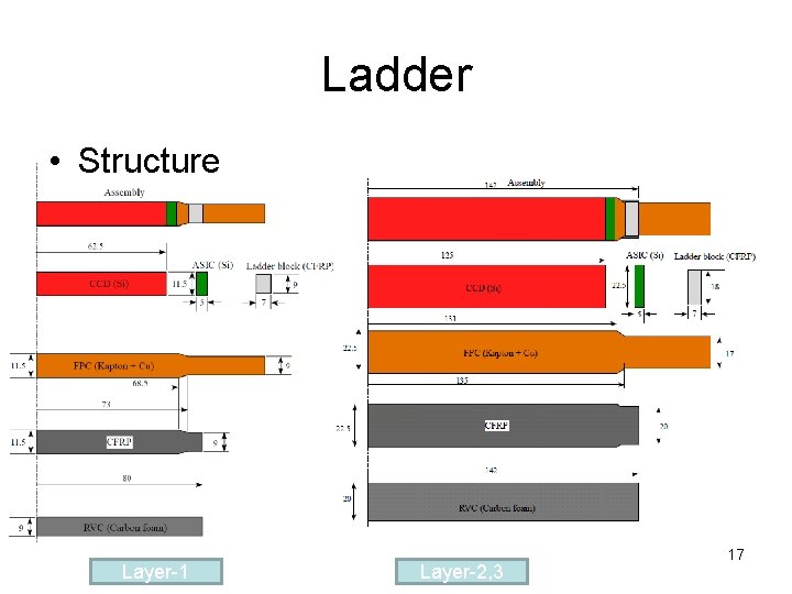
Ladder • Structure Layer-1 Layer-2, 3 17

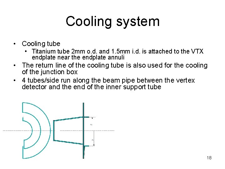
Cooling system • Cooling tube • Titanium tube 2 mm o. d. and 1. 5 mm i. d. is attached to the VTX endplate near the endplate annuli • The return line of the cooling tube is also used for the cooling of the junction box • 4 tubes/side run along the beam pipe between the vertex detector and the end of the inner support tube 18