Power 6 884 Spring 2005 3705 L 11

- Slides: 31

Power 6. 884 – Spring 2005 3/7/05 L 11 – Power 1

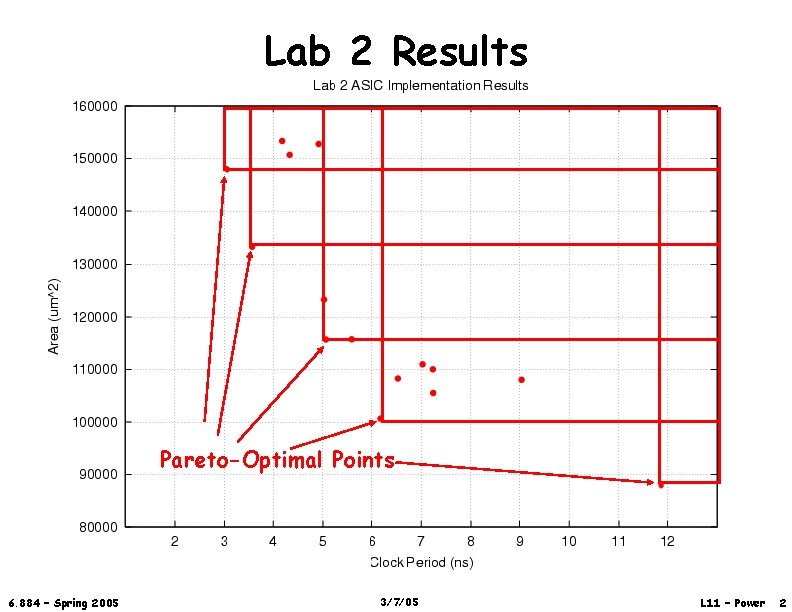
Lab 2 Results Pareto-Optimal Points 6. 884 – Spring 2005 3/7/05 L 11 – Power 2

Standard Projects § Two basic design projects – Processor variants (based on lab 1&2 testrigs) – Non-blocking caches and memory system – Possible project ideas on web site § Must hand in proposal before quiz on March 18 th, including: – Team members (2 or 3 per team) – Description of project, including the architecture exploration you will attempt 6. 884 – Spring 2005 3/7/05 L 11 – Power 3

Non-Standard Projects § Must hand in proposal early by class on March 14 th, describing: – Team members (2 or 3) – The chip you want to design – The existing reference code you will use to build a test rig, and the test strategy you will use – The architectural exploration you will attempt 6. 884 – Spring 2005 3/7/05 L 11 – Power 4

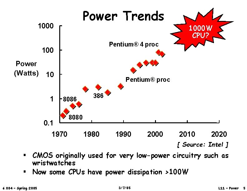
Power Trends 1000 Pentium® 4 proc 100 Power (Watts) 10 1 1000 W CPU? Pentium® proc 8086 0. 1 1970 386 8080 1990 2000 2010 2020 [ Source: Intel ] § CMOS originally used for very low-power circuitry such as wristwatches § Now some CPUs have power dissipation >100 W 6. 884 – Spring 2005 3/7/05 L 11 – Power 5

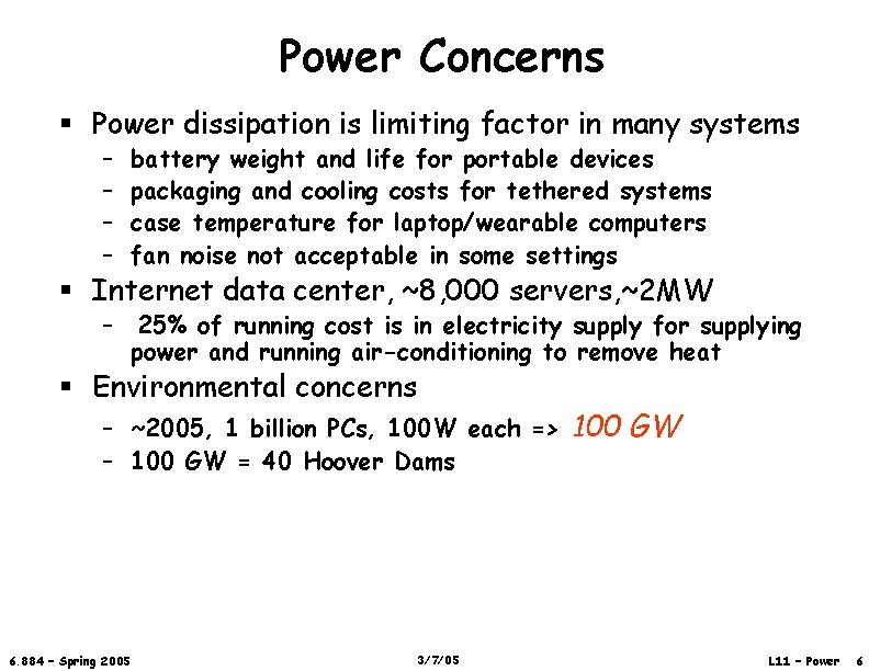
Power Concerns § Power dissipation is limiting factor in many systems – – battery weight and life for portable devices packaging and cooling costs for tethered systems case temperature for laptop/wearable computers fan noise not acceptable in some settings § Internet data center, ~8, 000 servers, ~2 MW – 25% of running cost is in electricity supply for supplying power and running air-conditioning to remove heat § Environmental concerns – ~2005, 1 billion PCs, 100 W each => – 100 GW = 40 Hoover Dams 6. 884 – Spring 2005 3/7/05 100 GW L 11 – Power 6

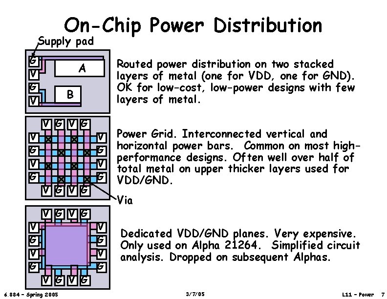
On-Chip Power Distribution Supply pad G V V G V G Routed power distribution on two stacked layers of metal (one for VDD, one for GND). OK for low-cost, low-power designs with few layers of metal. A B V G V G 6. 884 – Spring 2005 V G Power Grid. Interconnected vertical and horizontal power bars. Common on most highperformance designs. Often well over half of total metal on upper thicker layers used for VDD/GND. Via V G Dedicated VDD/GND planes. Very expensive. Only used on Alpha 21264. Simplified circuit analysis. Dropped on subsequent Alphas. 3/7/05 L 11 – Power 7

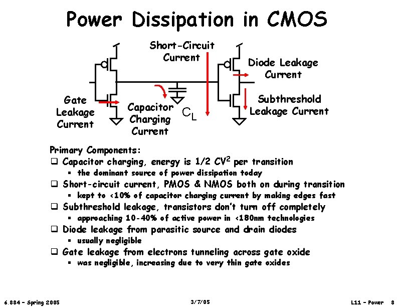
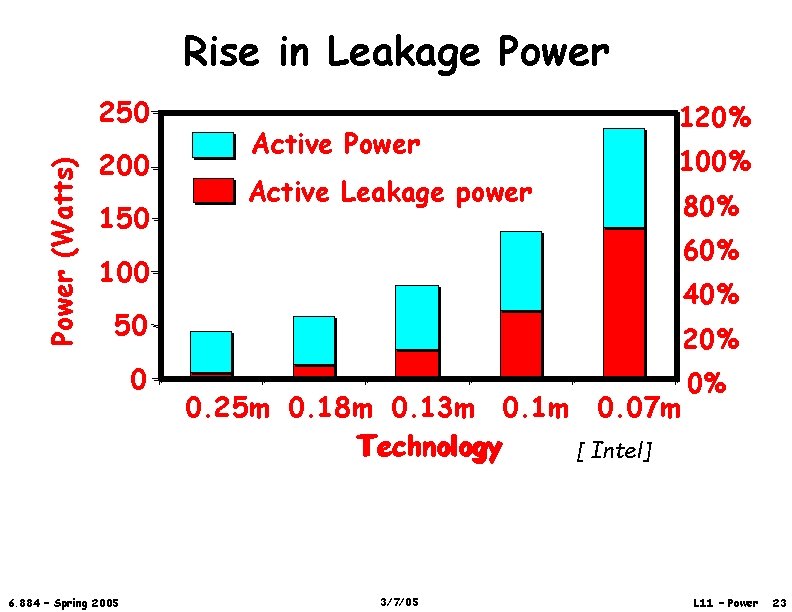
Power Dissipation in CMOS Short-Circuit Current Gate Leakage Current Capacitor Charging Current CL Diode Leakage Current Subthreshold Leakage Current Primary Components: q Capacitor charging, energy is 1/2 CV 2 per transition § the dominant source of power dissipation today q Short-circuit current, PMOS & NMOS both on during transition § kept to <10% of capacitor charging current by making edges fast q Subthreshold leakage, transistors don’t turn off completely § approaching 10 -40% of active power in <180 nm technologies q Diode leakage from parasitic source and drain diodes § usually negligible q Gate leakage from electrons tunneling across gate oxide § was negligible, increasing due to very thin gate oxides 6. 884 – Spring 2005 3/7/05 L 11 – Power 8

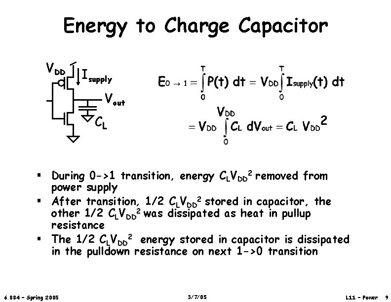
Energy to Charge Capacitor VDD Isupply Vout CL § During 0 ->1 transition, energy CLVDD 2 removed from power supply § After transition, 1/2 CLVDD 2 stored in capacitor, the other 1/2 CLVDD 2 was dissipated as heat in pullup resistance § The 1/2 CLVDD 2 energy stored in capacitor is dissipated in the pulldown resistance on next 1 ->0 transition 6. 884 – Spring 2005 3/7/05 L 11 – Power 9

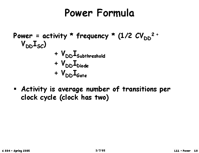
Power Formula Power = activity * frequency * (1/2 CVDD 2 + VDDISC) + VDDISubthreshold + VDDIDiode + VDDIGate § Activity is average number of transitions per clock cycle (clock has two) 6. 884 – Spring 2005 3/7/05 L 11 – Power 10

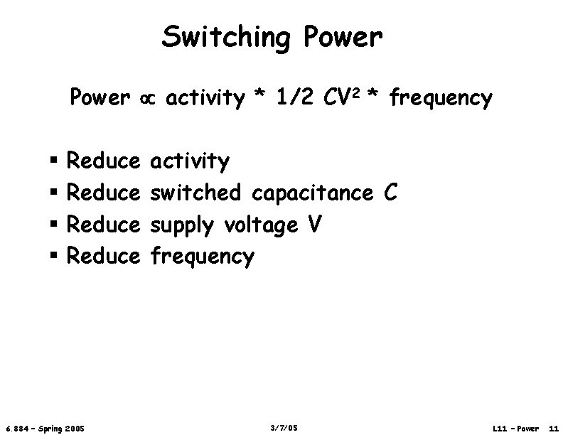
Switching Power activity * 1/2 CV 2 * frequency § § Reduce 6. 884 – Spring 2005 activity switched capacitance C supply voltage V frequency 3/7/05 L 11 – Power 11

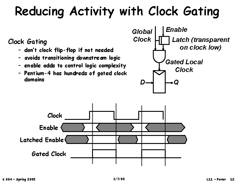
Reducing Activity with Clock Gating Global Clock Gating – – don’t clock flip-flop if not needed avoids transitioning downstream logic enable adds to control logic complexity Pentium-4 has hundreds of gated clock domains Enable Latch (transparent on clock low) Gated Local Clock D Q Clock Enable Latched Enable Gated Clock 6. 884 – Spring 2005 3/7/05 L 11 – Power 12

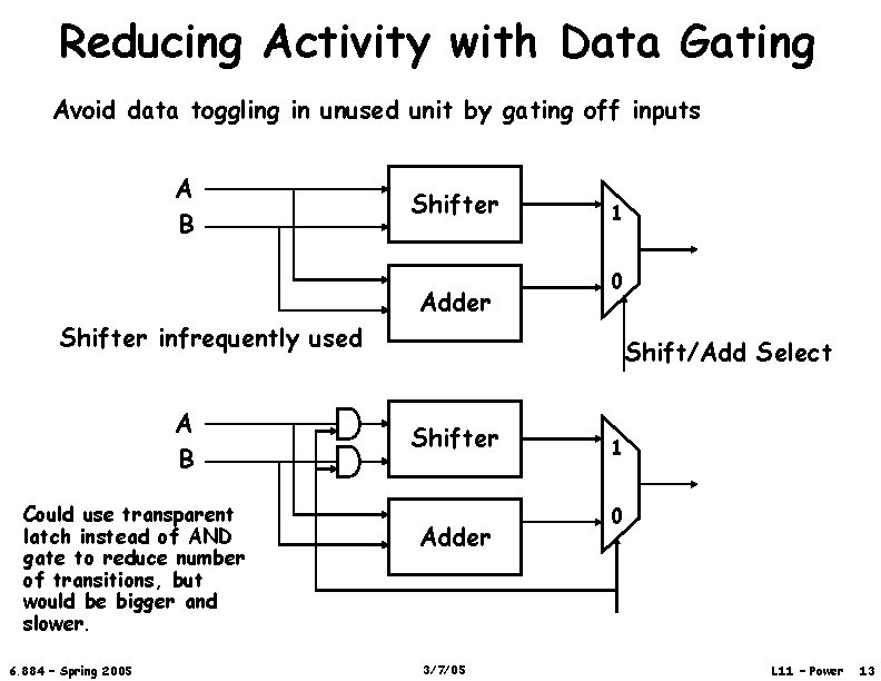
Reducing Activity with Data Gating Avoid data toggling in unused unit by gating off inputs A B Shifter Adder 1 0 Shifter infrequently used A B Could use transparent latch instead of AND gate to reduce number of transitions, but would be bigger and slower. 6. 884 – Spring 2005 Shift/Add Select Shifter Adder 3/7/05 1 0 L 11 – Power 13

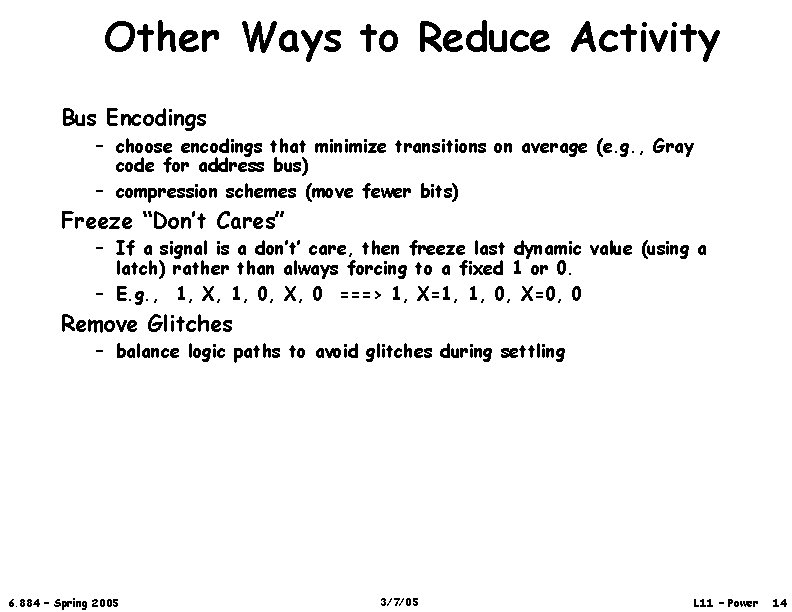
Other Ways to Reduce Activity Bus Encodings – choose encodings that minimize transitions on average (e. g. , Gray code for address bus) – compression schemes (move fewer bits) Freeze “Don’t Cares” – If a signal is a don’t’ care, then freeze last dynamic value (using a latch) rather than always forcing to a fixed 1 or 0. – E. g. , 1, X, 1, 0, X, 0 ===> 1, X=1, 1, 0, X=0, 0 Remove Glitches – balance logic paths to avoid glitches during settling 6. 884 – Spring 2005 3/7/05 L 11 – Power 14

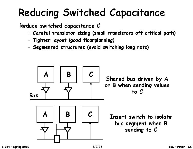
Reducing Switched Capacitance Reduce switched capacitance C – Careful transistor sizing (small transistors off critical path) – Tighter layout (good floorplanning) – Segmented structures (avoid switching long nets) A B C Bus 6. 884 – Spring 2005 Shared bus driven by A or B when sending values to C Insert switch to isolate bus segment when B sending to C 3/7/05 L 11 – Power 15

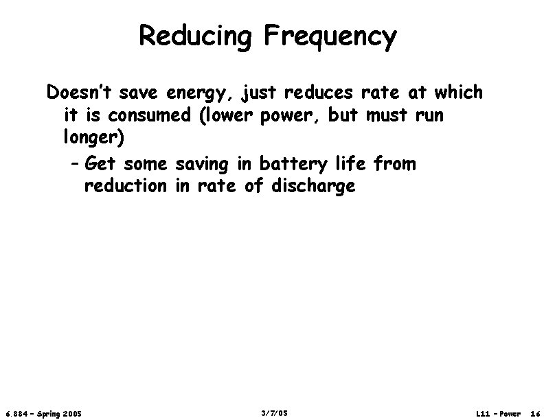
Reducing Frequency Doesn’t save energy, just reduces rate at which it is consumed (lower power, but must run longer) – Get some saving in battery life from reduction in rate of discharge 6. 884 – Spring 2005 3/7/05 L 11 – Power 16

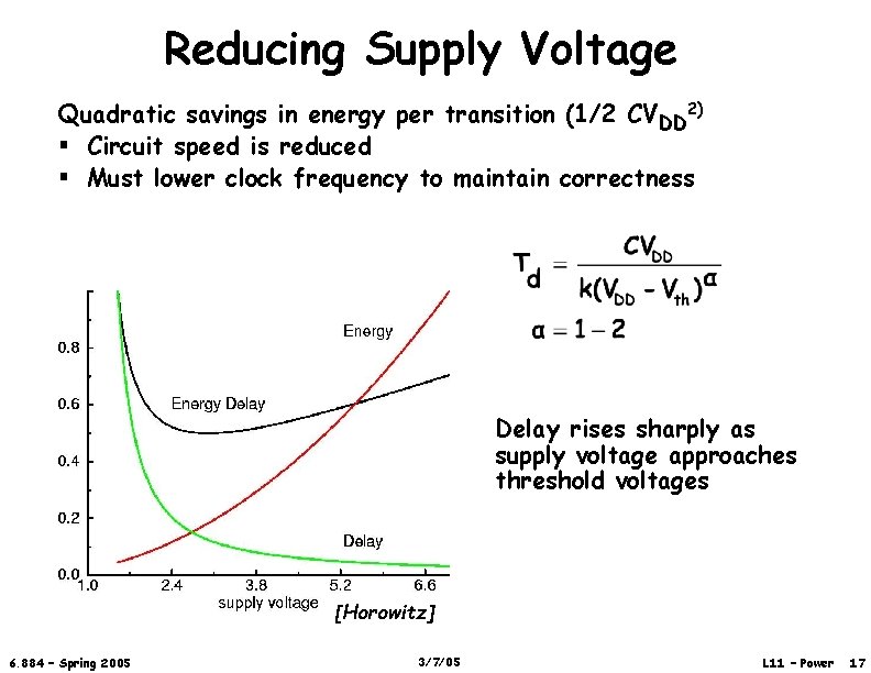
Reducing Supply Voltage Quadratic savings in energy per transition (1/2 CVDD 2) § Circuit speed is reduced § Must lower clock frequency to maintain correctness Delay rises sharply as supply voltage approaches threshold voltages [Horowitz] 6. 884 – Spring 2005 3/7/05 L 11 – Power 17

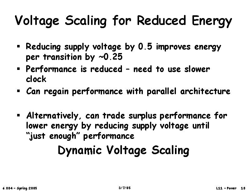
Voltage Scaling for Reduced Energy § Reducing supply voltage by 0. 5 improves energy per transition by ~0. 25 § Performance is reduced – need to use slower clock § Can regain performance with parallel architecture § Alternatively, can trade surplus performance for lower energy by reducing supply voltage until “just enough” performance Dynamic Voltage Scaling 6. 884 – Spring 2005 3/7/05 L 11 – Power 18

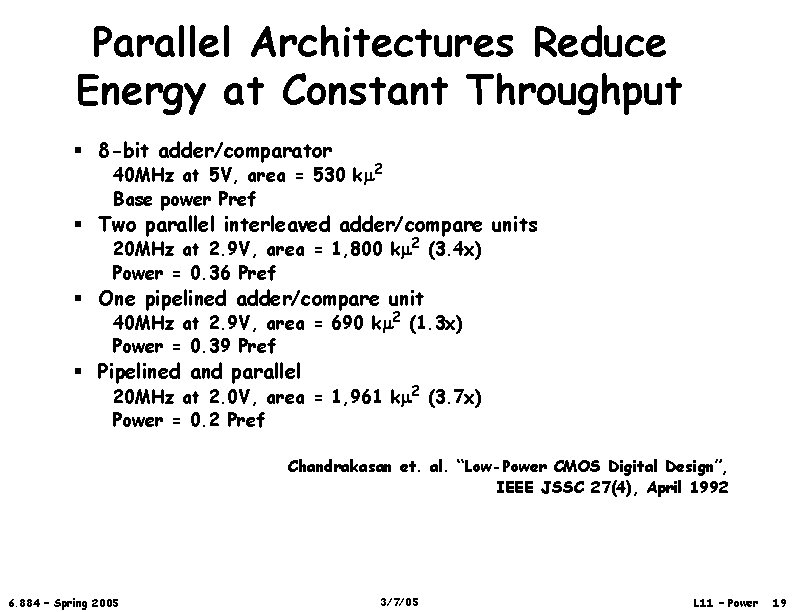
Parallel Architectures Reduce Energy at Constant Throughput § 8 -bit adder/comparator 40 MHz at 5 V, area = 530 km 2 Base power Pref § Two parallel interleaved adder/compare units 20 MHz at 2. 9 V, area = 1, 800 km 2 (3. 4 x) Power = 0. 36 Pref § One pipelined adder/compare unit 40 MHz at 2. 9 V, area = 690 km 2 (1. 3 x) Power = 0. 39 Pref § Pipelined and parallel 20 MHz at 2. 0 V, area = 1, 961 km 2 (3. 7 x) Power = 0. 2 Pref Chandrakasan et. al. “Low-Power CMOS Digital Design”, IEEE JSSC 27(4), April 1992 6. 884 – Spring 2005 3/7/05 L 11 – Power 19

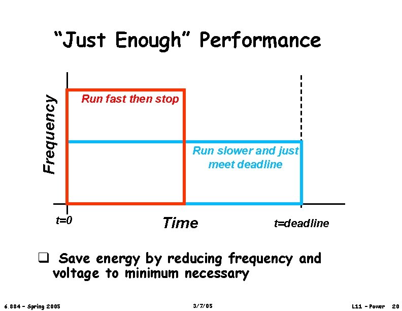
Frequency “Just Enough” Performance t=0 Run fast then stop Run slower and just meet deadline Time t=deadline q Save energy by reducing frequency and voltage to minimum necessary 6. 884 – Spring 2005 3/7/05 L 11 – Power 20

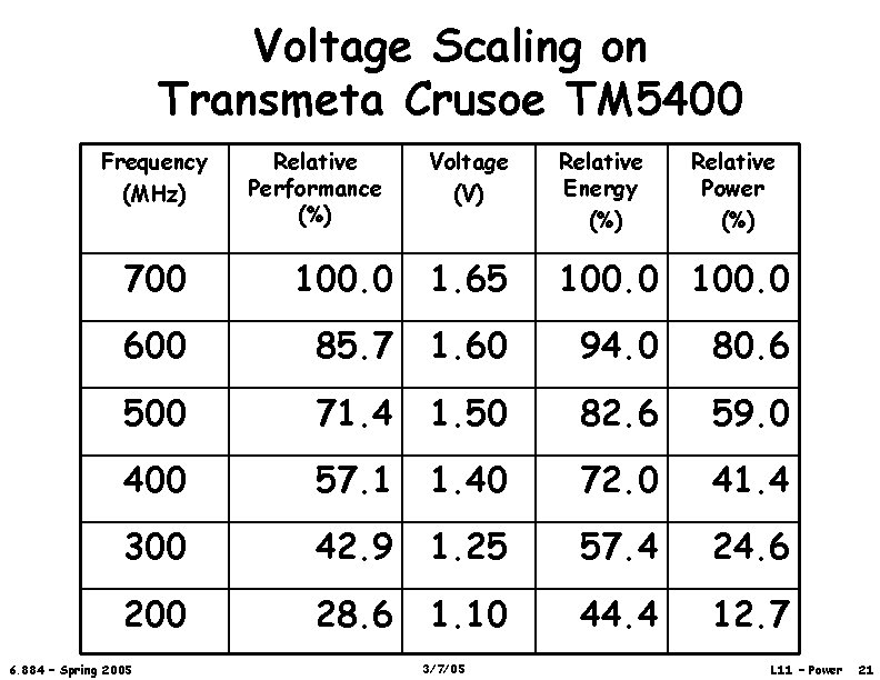
Voltage Scaling on Transmeta Crusoe TM 5400 Frequency (MHz) Relative Performance (%) Voltage (V) Relative Energy (%) Relative Power (%) 100. 0 700 100. 0 1. 65 600 85. 7 1. 60 94. 0 80. 6 500 71. 4 1. 50 82. 6 59. 0 400 57. 1 1. 40 72. 0 41. 4 300 42. 9 1. 25 57. 4 24. 6 200 28. 6 1. 10 44. 4 12. 7 6. 884 – Spring 2005 3/7/05 L 11 – Power 21

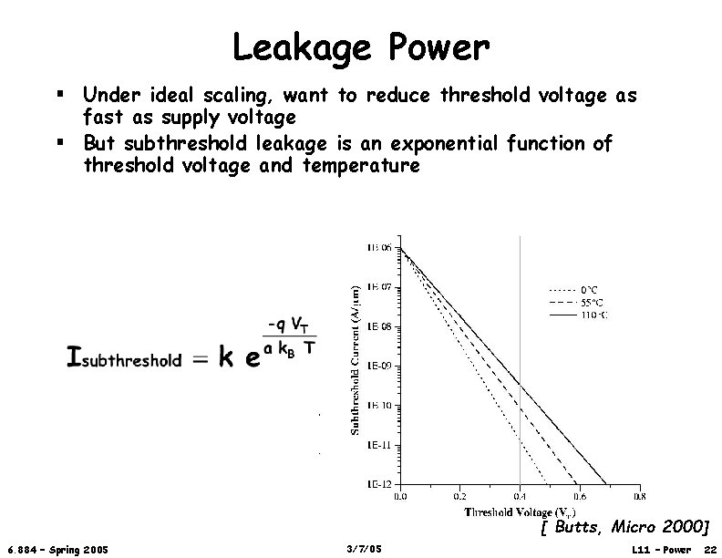
Leakage Power § Under ideal scaling, want to reduce threshold voltage as fast as supply voltage § But subthreshold leakage is an exponential function of threshold voltage and temperature [ Butts, Micro 2000] 6. 884 – Spring 2005 3/7/05 L 11 – Power 22

Rise in Leakage Power (Watts) 250 200 150 Active Power Active Leakage power 120% 100% 60% 100 40% 50 0 6. 884 – Spring 2005 80% 20% 0. 25 m 0. 18 m 0. 13 m 0. 1 m 0. 07 m Technology [ Intel] 3/7/05 0% L 11 – Power 23

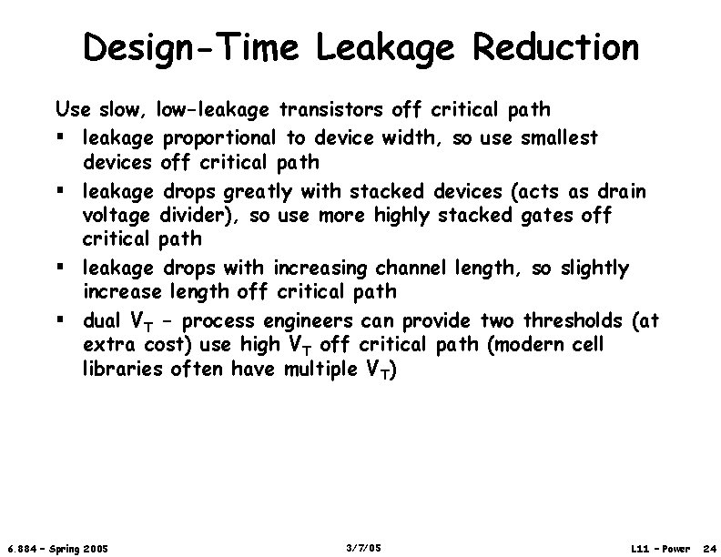
Design-Time Leakage Reduction Use slow, low-leakage transistors off critical path § leakage proportional to device width, so use smallest devices off critical path § leakage drops greatly with stacked devices (acts as drain voltage divider), so use more highly stacked gates off critical path § leakage drops with increasing channel length, so slightly increase length off critical path § dual VT - process engineers can provide two thresholds (at extra cost) use high VT off critical path (modern cell libraries often have multiple VT) 6. 884 – Spring 2005 3/7/05 L 11 – Power 24

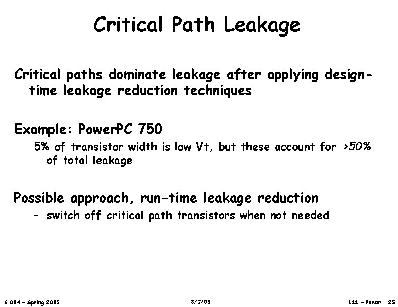
Critical Path Leakage Critical paths dominate leakage after applying designtime leakage reduction techniques Example: Power. PC 750 5% of transistor width is low Vt, but these account for >50% of total leakage Possible approach, run-time leakage reduction – switch off critical path transistors when not needed 6. 884 – Spring 2005 3/7/05 L 11 – Power 25

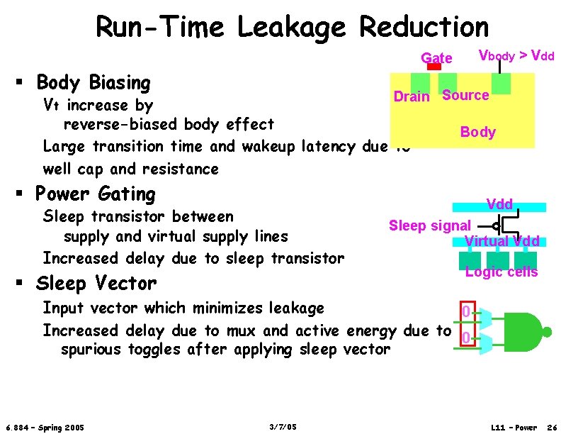
Run-Time Leakage Reduction Vbody > Vdd Gate § Body Biasing Drain Source Vt increase by reverse-biased body effect Large transition time and wakeup latency due to well cap and resistance Body § Power Gating Sleep transistor between supply and virtual supply lines Increased delay due to sleep transistor § Sleep Vector Vdd Sleep signal Virtual Vdd Logic cells Input vector which minimizes leakage 0 Increased delay due to mux and active energy due to 0 spurious toggles after applying sleep vector 6. 884 – Spring 2005 3/7/05 L 11 – Power 26

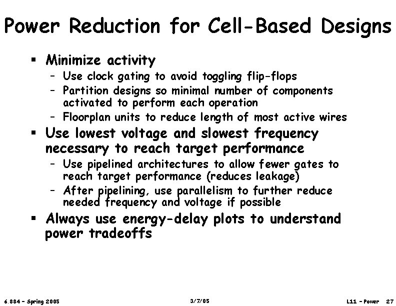
Power Reduction for Cell-Based Designs § Minimize activity – Use clock gating to avoid toggling flip-flops – Partition designs so minimal number of components activated to perform each operation – Floorplan units to reduce length of most active wires § Use lowest voltage and slowest frequency necessary to reach target performance – Use pipelined architectures to allow fewer gates to reach target performance (reduces leakage) – After pipelining, use parallelism to further reduce needed frequency and voltage if possible § Always use energy-delay plots to understand power tradeoffs 6. 884 – Spring 2005 3/7/05 L 11 – Power 27

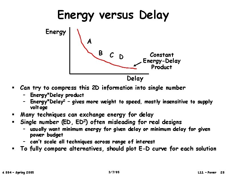
Energy versus Delay Energy A B C D Constant Energy-Delay Product Delay § Can try to compress this 2 D information into single number § § Many techniques can exchange energy for delay Single number (ED, ED 2) often misleading for real designs § To fully compare alternatives, should plot E-D curve for each solution – Energy*Delay product – Energy*Delay 2 – gives more weight to speed, mostly insensitive to supply voltage – usually want minimum energy for given delay or minimum delay for given power budget – can’t scale all techniques across range of interest 6. 884 – Spring 2005 3/7/05 L 11 – Power 28

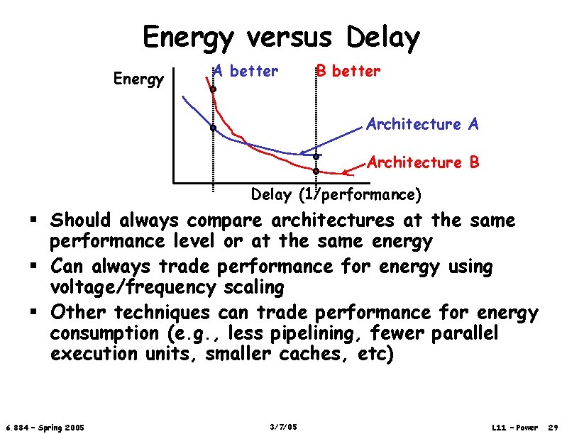
Energy versus Delay Energy A better B better Architecture A Architecture B Delay (1/performance) § Should always compare architectures at the same performance level or at the same energy § Can always trade performance for energy using voltage/frequency scaling § Other techniques can trade performance for energy consumption (e. g. , less pipelining, fewer parallel execution units, smaller caches, etc) 6. 884 – Spring 2005 3/7/05 L 11 – Power 29

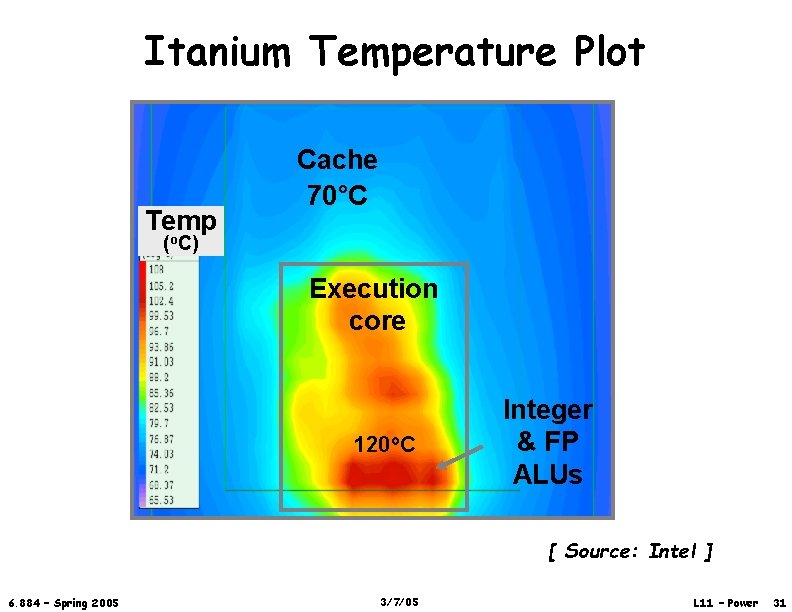
Temperature Hot Spots § Not just total power, but power density is a problem for modern high-performance chips § Some parts of the chip get much hotter than others – Transistors get slower when hotter – Leakage gets exponentially worse (can get thermal runaway with positive feedback between temperature and leakage power) – Chip reliability suffers § Few good solutions as yet – Better floorplanning to spread hot units across chip – Activity migration, to move computation from hot units to cold units – More expensive packaging (liquid cooling) 6. 884 – Spring 2005 3/7/05 L 11 – Power 30

Itanium Temperature Plot Temp Cache 70°C (o. C) Execution core 120 o. C Integer & FP ALUs [ Source: Intel ] 6. 884 – Spring 2005 3/7/05 L 11 – Power 31