OPTICAL COMMUNICATION CIRCUITS WAVEGUIDES Lecture 4 th CONTENTS

- Slides: 50

OPTICAL COMMUNICATION CIRCUITS & WAVEGUIDES Lecture 4 th

CONTENTS • Integrated Optical Circuits (OIC) • Optical signal processing • Optical filters • Optical Couplers • Optical Modulators • Optical Wavelength Converters

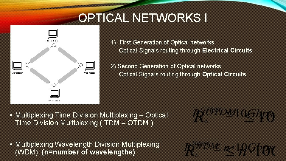
OPTICAL NETWORKS I 1) First Generation of Optical networks Optical Signals routing through Electrical Circuits 2) Second Generation of Optical networks Optical Signals routing through Optical Circuits • Multiplexing Time Division Multiplexing – Optical Time Division Multiplexing ( TDM – OTDM ) • Multiplexing Wavelength Division Multiplexing (WDM) (n=number of wavelengths)

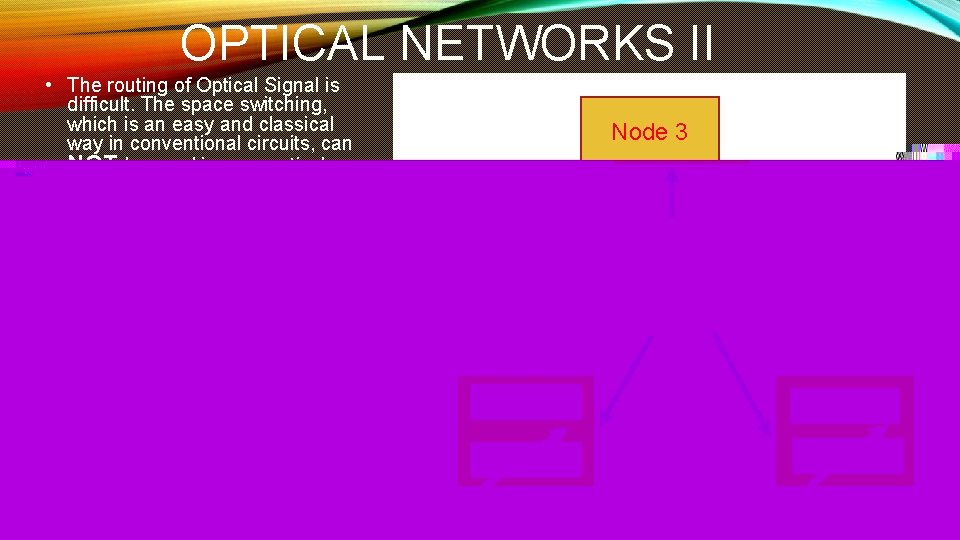
OPTICAL NETWORKS II • The routing of Optical Signal is difficult. The space switching, which is an easy and classical way in conventional circuits, can NOT be used in pure optical networks. • Wavelength Multiplexing gives the ability of choοsing a specific wavelength and give an extra degree of freedom in the system. • The chosen wavelength can be used for the routing of data. • Two categories of 2 nd generation of networks, which use multiplexing for signal routing through the nodes 1. Broadcast and Select Networks (BS) 2. Wavelength Routing (WR) Node 3 Star coupler Node 2 Node 3 LASER RECEIVER

BASIC COMPONENTS OF OPTICAL CIRCUITS • Optical Filters • Space Switching • Wavelength Converters • Modulators • Optical Sources (LED & Lasers) • Optical Receivers Φωτοδέκτες • Optical Amplifiers

BASIC COMPONENTS OF OPTICAL CIRCUITS • The dimensions and materials of the circuit’s waveguides is of crucial importance for the correct function of the network Homojunctions Heterojunctions

OPTICAL FILTERS AND SWITCHES • Each node of the network must combine ALL the wavelengths in one signal and routes the optical signal in an optical fiber (multiplexing). Moreover, each node must separate the wavelengths which end up at the node, through the optical fiber (Demultiplexing). 1. 2. 3. 4. 5. 6. Diffraction gratings Bragg gratings Mach Zender Interferometer Thin layer filters Fabry-Perot filters Arrayed Waveguide Grating (AWG)

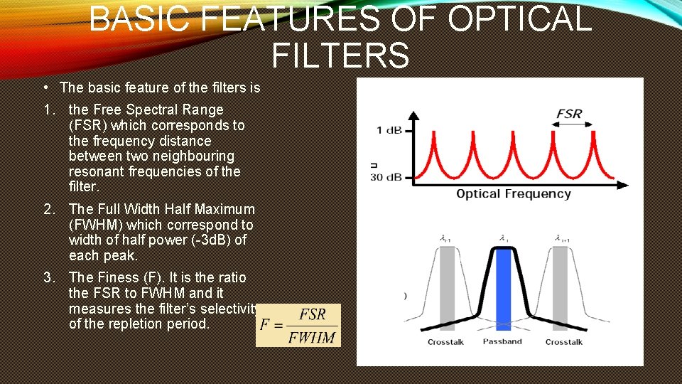
BASIC FEATURES OF OPTICAL FILTERS • The basic feature of the filters is 1. the Free Spectral Range (FSR) which corresponds to the frequency distance between two neighbouring resonant frequencies of the filter. 2. The Full Width Half Maximum (FWHM) which correspond to width of half power (-3 d. B) of each peak. 3. The Finess (F). It is the ratio the FSR to FWHM and it measures the filter’s selectivity of the repletion period.

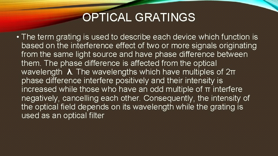
OPTICAL GRATINGS • The term grating is used to describe each device which function is based on the interference effect of two or more signals originating from the same light source and have phase difference between them. The phase difference is affected from the optical wavelength λ. The wavelengths which have multiples of 2π phase difference interfere positively and their intensity is increased while those who have an odd multiple of π interfere negatively, cancelling each other. Consequently, the intensity of the optical field depends on its wavelength while the grating is used as an optical filter

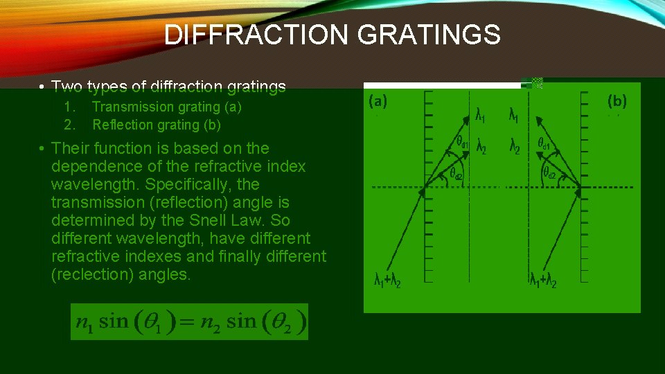
DIFFRACTION GRATINGS • Two types of diffraction gratings 1. 2. Transmission grating (a) Reflection grating (b) • Their function is based on the dependence of the refractive index wavelength. Specifically, the transmission (reflection) angle is determined by the Snell Law. So different wavelength, have different refractive indexes and finally different (reclection) angles. (a) (b) on the transmission

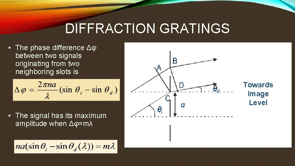
DIFFRACTION GRATINGS • The phase difference Δφ between two signals originating from two neighboring slots is Towards Image Level • The signal has its maximum amplitude when Δφ=mλ

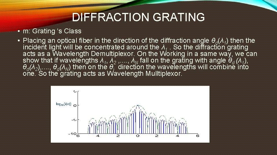
DIFFRACTION GRATING • m: Grating ‘s Class • Placing an optical fiber in the direction of the diffraction angle θd(λ 1) then the incident light will be concentrated around the λ 1. So the diffraction grating acts as a Wavelength Demultiplexor. On the Working in a same way, we can show that if wavelengths λ 1, λ 2 , . . , λN fall on the grating with angle θd (λ 1), θd(λ 2), . . , θd(λN) then on the θi direction the wavelengths will combine into one. So the grating acts as Wavelength Mulltiplexor.

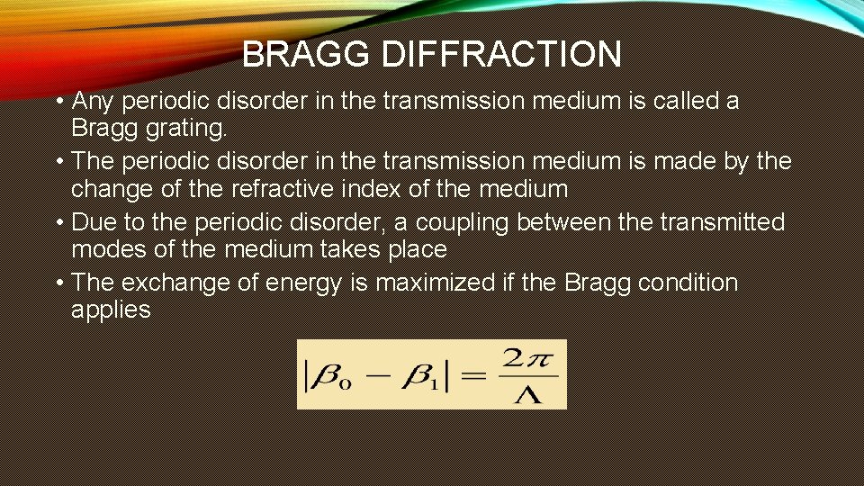
BRAGG DIFFRACTION • Any periodic disorder in the transmission medium is called a Bragg grating. • The periodic disorder in the transmission medium is made by the change of the refractive index of the medium • Due to the periodic disorder, a coupling between the transmitted modes of the medium takes place • The exchange of energy is maximized if the Bragg condition applies

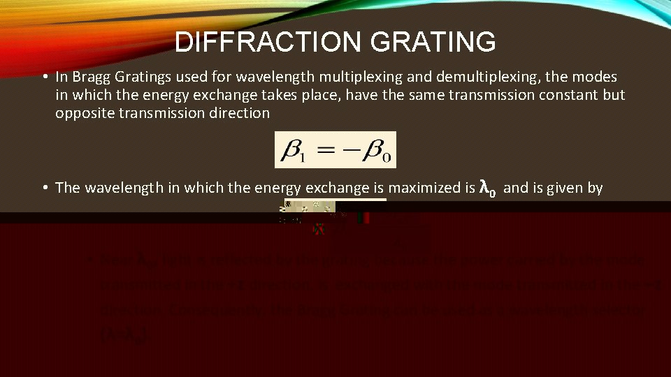
DIFFRACTION GRATING • In Bragg Gratings used for wavelength multiplexing and demultiplexing, the modes in which the energy exchange takes place, have the same transmission constant but opposite transmission direction • The wavelength in which the energy exchange is maximized is λ 0 and is given by • Near λ 0, light is reflected by the grating because the power carried by the mode transmitted in the +z direction, is exchanged with the mode transmitted in the –z direction. Consequently, the Bragg Grating can be used as a wavelength selector (λ=λ 0).

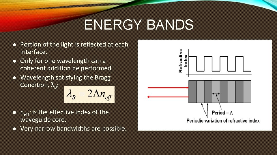
ENERGY BANDS l l l Portion of the light is reflected at each interface. Only for one wavelength can a coherent addition be performed. Wavelength satisfying the Bragg Condition, λB: neff: is the effective index of the waveguide core. Very narrow bandwidths are possible.

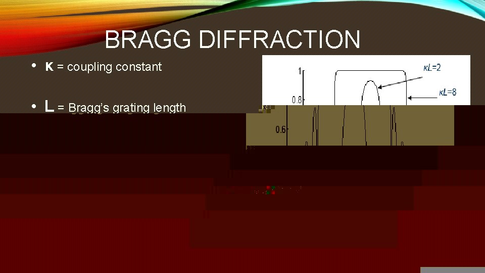
BRAGG DIFFRACTION • κ = coupling constant • L = Bragg’s grating length

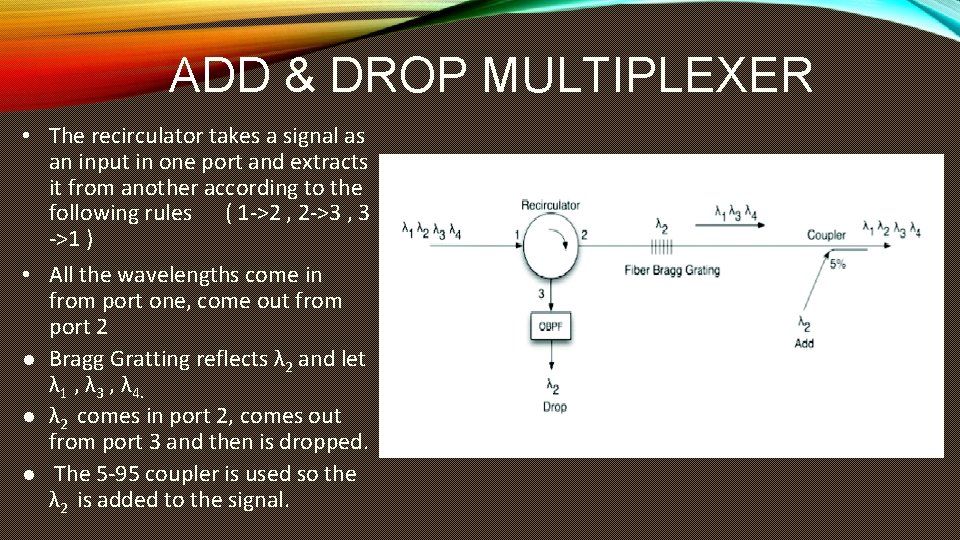
ADD & DROP MULTIPLEXER • The recirculator takes a signal as an input in one port and extracts it from another according to the following rules ( 1 ->2 , 2 ->3 , 3 ->1 ) • All the wavelengths come in from port one, come out from port 2 l Bragg Gratting reflects λ 2 and let λ 1 , λ 3 , λ 4. l λ 2 comes in port 2, comes out from port 3 and then is dropped. l The 5 -95 coupler is used so the λ 2 is added to the signal.

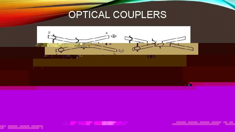
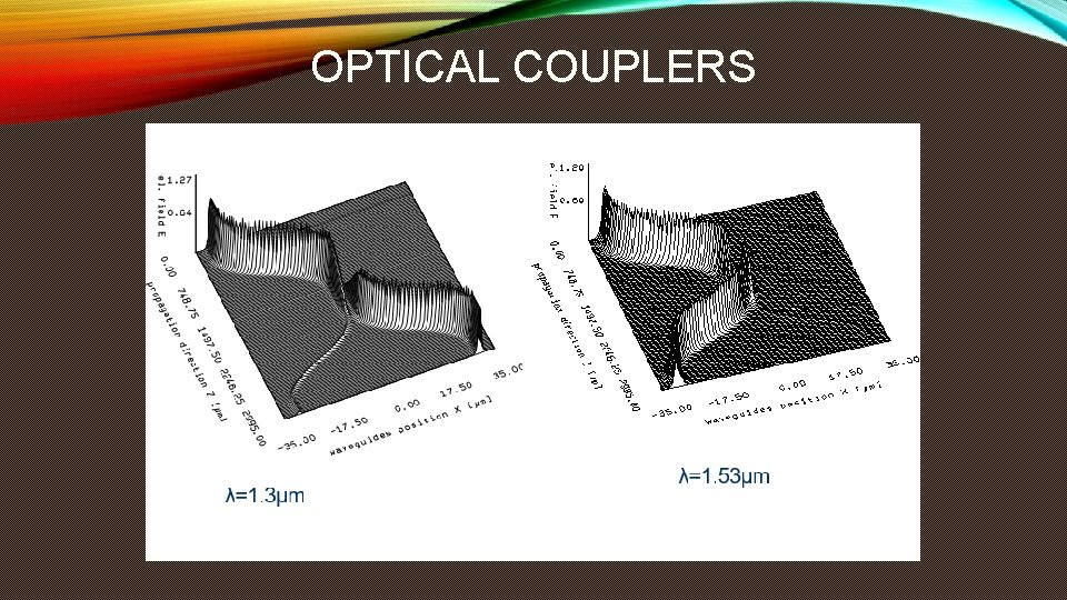
OPTICAL COUPLERS • The directional coupler is a simple flexible structure. It can be used as 1. 2. 3. 4. Optical power splitter Wavelength filter Selector or Converters of polarization Switcher for the routing of the optical signals • The directional coupler is consisted of parallel, single-mode waveguides, placed in close distance. • The optical power inserted in one waveguide, is transferred in the other waveguide, as a consequence of the overlapping of the damped optical Fields of the two singlemoded waveguides.

OPTICAL COUPLERS

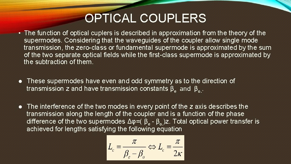
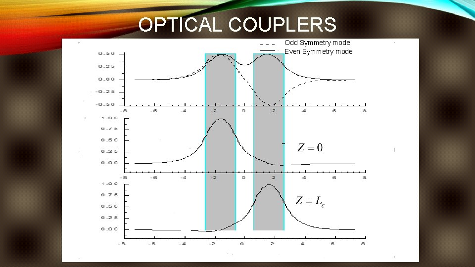
OPTICAL COUPLERS • The function of optical cuplers is described in approximation from theory of the supermodes. Considering that the waveguides of the coupler allow single mode transmission, the zero-class or fundamental supermode is approximated by the sum of the two separate optical fields while the first-class supermode is approximated by the subtraction of them. l These supermodes have even and odd symmetry as to the direction of transmission z and have transmission constants βe and βo. . l The interference of the two modes in every point of the z axis describes the transmission along the length of the coupler and is a function of the phase difference of the two supermodes Δφ=( βe - βo. )z. Total optical power transfer is achieved for lengths satisfying the following equation

OPTICAL COUPLERS Odd Symmetry mode Even Symmetry mode

OPTICAL COUPLERS

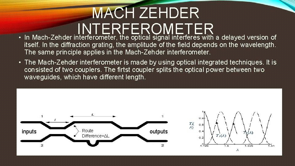
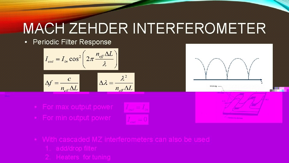
MACH ZEHDER INTERFEROMETER • In Mach-Zehder interferometer, the optical signal interferes with a delayed version of itself. In the diffraction grating, the amplitude of the field depends on the wavelength. The same principle applies in the Mach-Zehder interferometer. • The Mach-Zehder interferometer is made by using optical integrated techniques. It is consisted of two couplers. The firtst coupler splits the optical power between two waveguides, which have different length. inputs Route Difference=ΔL outputs

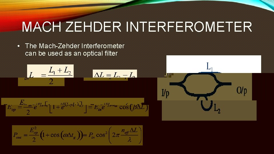
MACH ZEHDER INTERFEROMETER • The Mach-Zehder Interferometer can be used as an optical filter

MACH ZEHDER INTERFEROMETER • Periodic Filter Response • For max output power • For min output power • With cascaded MZ interferometers can also be used 1. add/drop filter 2. Heaters for tuning

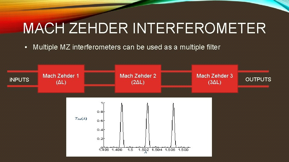
MACH ZEHDER INTERFEROMETER • Multiple MZ interferometers can be used as a multiple filter i. NPUTS Mach Zehder 1 (ΔL) Mach Zehder 2 (2ΔL) Mach Zehder 3 (3ΔL) OUTPUTS

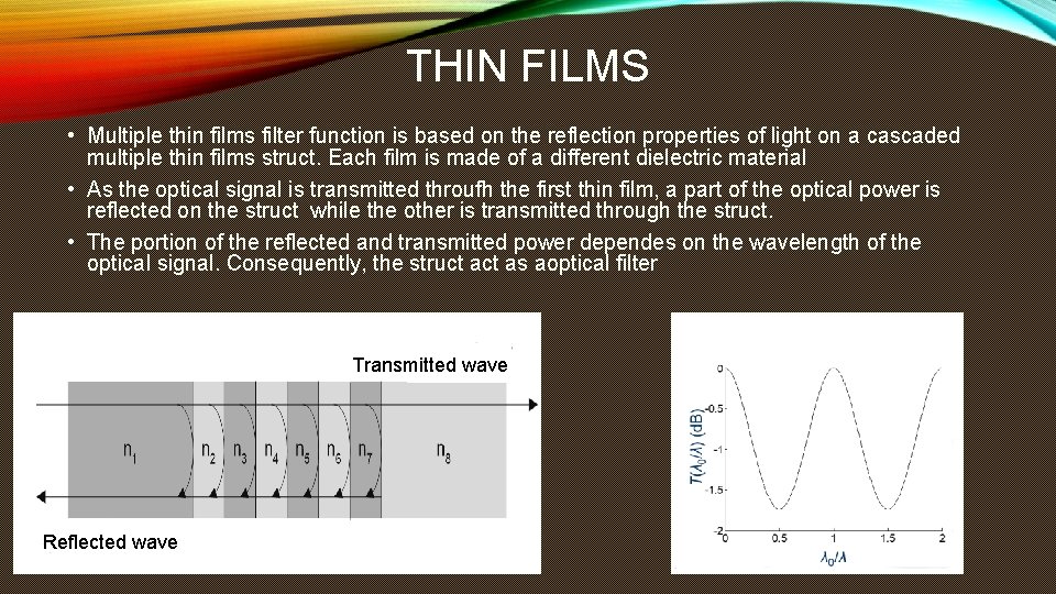
THIN FILMS • Multiple thin films filter function is based on the reflection properties of light on a cascaded multiple thin films struct. Each film is made of a different dielectric material • As the optical signal is transmitted throufh the first thin film, a part of the optical power is reflected on the struct while the other is transmitted through the struct. • The portion of the reflected and transmitted power dependes on the wavelength of the optical signal. Consequently, the struct as aoptical filter Transmitted wave Reflected wave

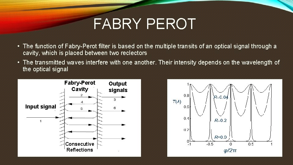
FABRY PEROT • The function of Fabry-Perot filter is based on the multiple transits of an optical signal through a cavity, which is placed between two reclectors • The transmitted waves interfere with one another. Their intensity depends on the wavelength of the optical signal Fabry-Perot Cavity Input signal Consecutive Reflections Output signals

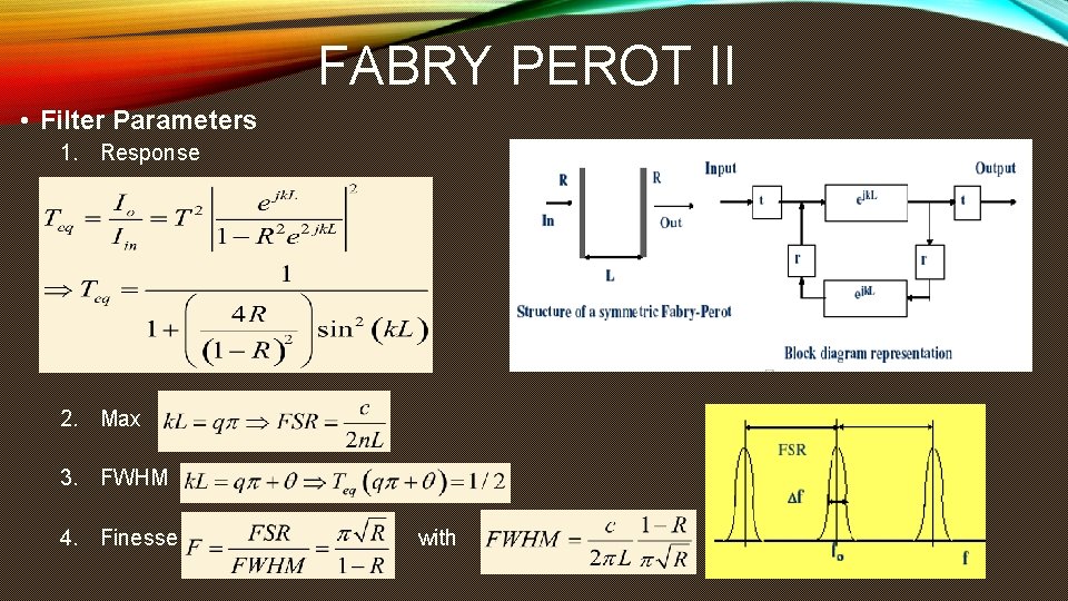
FABRY PEROT ΙΙ • Filter Parameters 1. Response 2. Max 3. FWHM 4. Finesse with

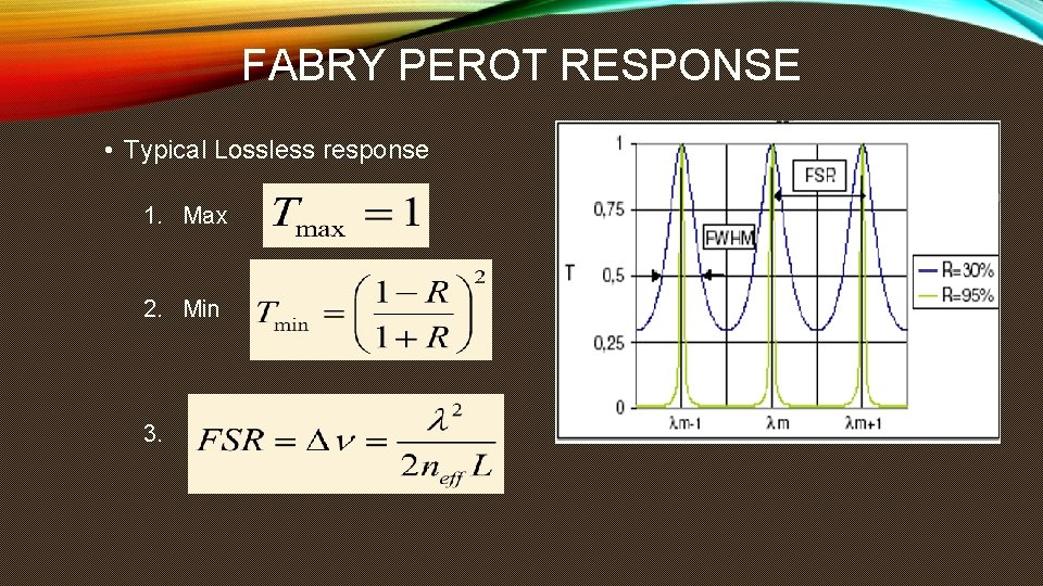
FABRY PEROT RESPONSE • Typical Lossless response 1. Max 2. Min 3.

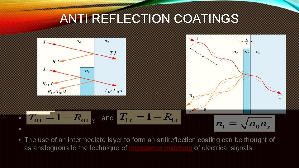
ANTI REFLECTION COATINGS • • T 01 = 1 -R 01 και T 1 S and • The use of an intermediate layer to form an antireflection coating can be thought of as analoguous to the technique of impedance matching of electrical signals

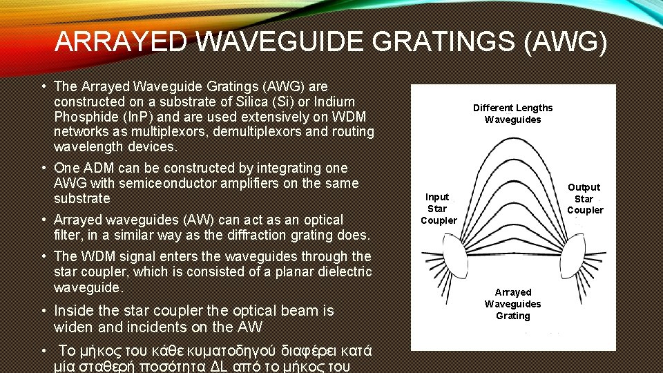
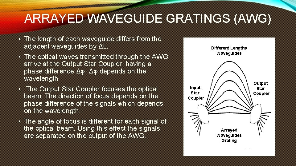
ARRAYED WAVEGUIDE GRATINGS (AWG) • The Arrayed Waveguide Gratings (AWG) are constructed on a substrate of Silica (Si) or Indium Phosphide (In. P) and are used extensively on WDM networks as multiplexors, demultiplexors and routing wavelength devices. • One ADM can be constructed by integrating one AWG with semiceonductor amplifiers on the same substrate • Arrayed waveguides (AW) can act as an optical filter, in a similar way as the diffraction grating does. • The WDM signal enters the waveguides through the star coupler, which is consisted of a planar dielectric waveguide. • Inside the star coupler the optical beam is widen and incidents on the AW • Το μήκος του κάθε κυματοδηγού διαφέρει κατά μία σταθερή ποσότητα ΔL από το μήκος του Different Lengths Waveguides Output Star Coupler Input Star Coupler Arrayed Waveguides Grating

ARRAYED WAVEGUIDE GRATINGS (AWG) • The length of each waveguide differs from the adjacent waveguides by ΔL. Different Lengths Waveguides • The optical waves transmitted through the AWG arrive at the Output Star Coupler, having a phase difference Δφ. Δφ depends on the wavelength • The Output Star Coupler focuses the optical beam. The direction of focus depends on the phase difference of the signals which depends on the wavelength. • The angle of focus is different for each signal of the optical beam. Using this effect the signals are separated on the output of the AWG. Output Star Coupler Input Star Coupler Arrayed Waveguides Grating

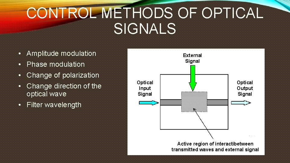
CONTROL METHODS OF OPTICAL SIGNALS • • Amplitude modulation Phase modulation Change of polarization Change direction of the optical wave • Filter wavelength External Signal Optical Input Signal Optical Output Signal Active region of interactibetween transmitted waves and external signal

CONTROL METHODS OF OPTICAL SIGNALS Ι • Opticoacoustical control. By using elastical surface waves (acoustic), the refractive index of a proper crystal changes (Zn. O, Li. Nb. O 3). The source of the control waves is a piezoelectric material, which is stimulated by electric signals. Because the longitudinal waves, as the acoustic waves, show periodic compression and rarefaction, the change of the refractive index of the crystal exhibits the same periodicity. This method is used to produce diffraction gratings with many applications. • Thermoptical control. The dependence of the refractive index of a specific group of materials is very strong. For example, the refractive index of Li. Nb. O 3 increases 5 to 10 when the temperature increases from 25 to 100 degree C. This effect, is known as thermoptical effect and is observed in all the transparent dielectrics and all materials used for optical integration. In semiconductor devices of III-V this effect is used in the construction of arrayed switching. But the speed of switching was constricted in 1 ms because of the non zero thermocapacitance of these devices.

CONTROL METHODS OF OPTICAL SIGNALS ΙΙ • Opticomagnetic control is based on the opticomagnetic effect, which affects the crystal ’s refractive index under the effect of α magnetic field. In this case, the crystal ‘s dielectric tensor loses its symmetry and the principle of reciprocity of the course of light, no longer applies. The devices based on this type of control are used mainly as optical isolators. • Electrooptical control. In this case, the refractive ondex of the crystal is changed by the fluctuations of an external electric field. The electroptical effect is used on hybrid structures of Li. Nb. O 3 and on similar monolithic integrated devices. The electroptical effect in Li. Nb. O 3 devices is extremely strong. • Electrooptical absorption. The effect of an external electric field on the interband absorption and for photon energy very close to the Energy Gap of the semiconductor is expressed thoufh the Franz-Keldysh and Stark effect.

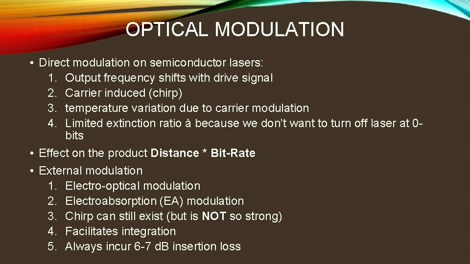
OPTICAL MODULATION • Direct modulation on semiconductor lasers: 1. Output frequency shifts with drive signal 2. Carrier induced (chirp) 3. temperature variation due to carrier modulation 4. Limited extinction ratio à because we don’t want to turn off laser at 0 bits • Effect on the product Distance * Bit-Rate • External modulation 1. Electro-optical modulation 2. Electroabsorption (EA) modulation 3. Chirp can still exist (but is NOT so strong) 4. Facilitates integration 5. Always incur 6 -7 d. B insertion loss

ADVANTAGES – DISADVANTAGES • Direct 1. Simple 2. Cost-effective 3. Compact • External 1. 2. 3. 4. 5. 6. Additional Component Additional Loss Higher Speed Large extinction ratio Low chirp Low modulation distortion

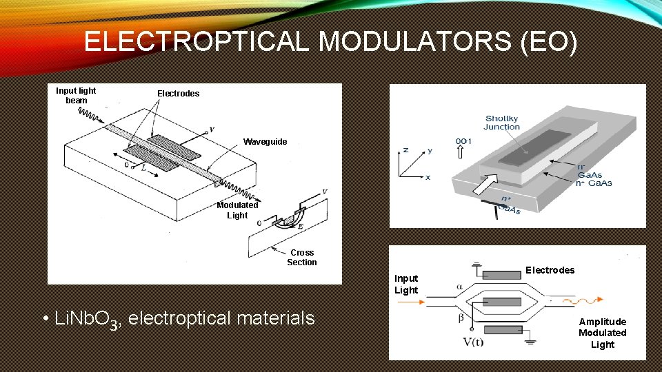
ELECTROPTICAL MODULATORS (EO) Input light beam Electrodes Waveguide Modulated Light Cross Section Input Light • Li. Nb. O 3, electroptical materials Electrodes Amplitude Modulated Light

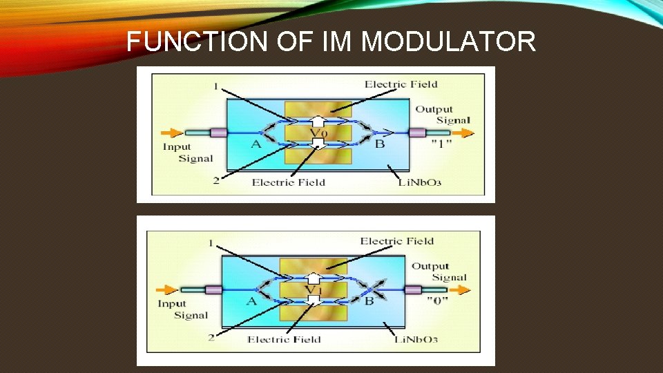
FUNCTION OF IM MODULATOR

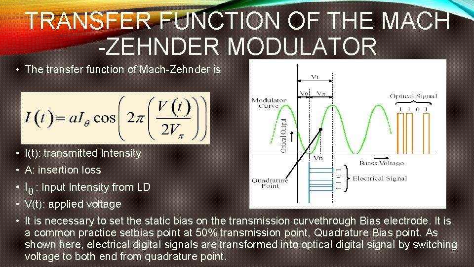
TRANSFER FUNCTION OF THE MACH -ZEHNDER MODULATOR • The transfer function of Mach-Zehnder is • I(t): transmitted Intensity • A: insertion loss • Iθ : Input Intensity from LD • V(t): applied voltage • It is necessary to set the static bias on the transmission curvethrough Bias electrode. It is a common practice setbias point at 50% transmission point, Quadrature Bias point. As shown here, electrical digital signals are transformed into optical digital signal by switching voltage to both end from quadrature point.

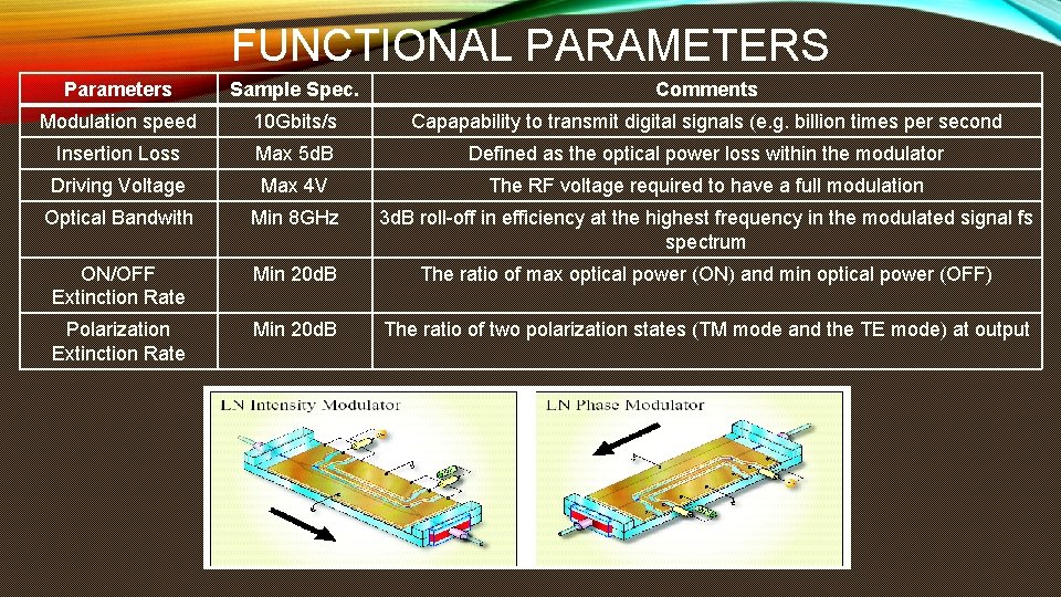
FUNCTIONAL PARAMETERS Parameters Sample Spec. Comments Modulation speed 10 Gbits/s Capapability to transmit digital signals (e. g. billion times per second Insertion Loss Max 5 d. B Defined as the optical power loss within the modulator Driving Voltage Max 4 V The RF voltage required to have a full modulation Optical Bandwith Min 8 GHz 3 d. B roll-off in efficiency at the highest frequency in the modulated signal fs spectrum ON/OFF Extinction Rate Min 20 d. B The ratio of max optical power (ON) and min optical power (OFF) Polarization Extinction Rate Min 20 d. B The ratio of two polarization states (TM mode and the TE mode) at output

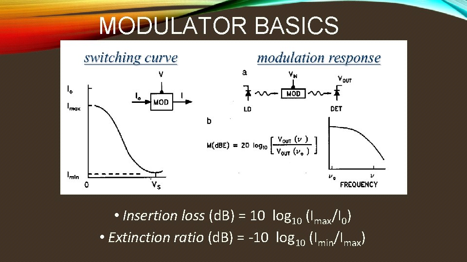
MODULATOR BASICS • Insertion loss (d. B) = 10 log 10 (Imax/I 0) • Extinction ratio (d. B) = -10 log 10 (Imin/Imax)

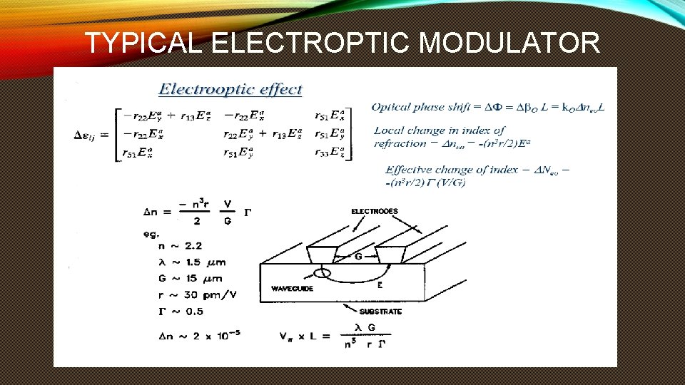
TYPICAL ELECTROPTIC MODULATOR

ELECTROABSORPTION (EA) MODULATOR • EA modulator is a semiconductor device • Typically has the same structure as the laser diode. • Use an applied electric field (reverse bias) to change the absorption spectrum. ØAbsorption spectrum changes with applied electric field Franz -Keldysh Effect • Extinction ratio enhancement in quantum well structures ØQuantum confined Stark effect

SCHEMATICS OF AN EA MODULATOR External electric field effects the attenuation coefficient

EA ABSORBER ADVANTAGES • Zero biasing voltage • Low driving voltage • Low/negative chirp • High speed • Integrated with DFB

WAVELENGTH CONVERTERS • Opticoelectric conversion. In optoelectric converters, the optic signal is converted in an electrical signal, which modulates a LASER, which is tuned to a specific wavelength • Gain Modulation in SOA. The gain of a SOA depends on the power of the signal which is inserted in the SOA. Due to the dependence of the amplifier ‘s gain on the wavelength of the signal, a monochromatic signal of wavelength λ 1 has its amplitude modulated from another signal on another wavelength λ 2, so the information on the λ 2 signal wavelength is transferred on the of λ 1 signal. • Phase Modulation in SOA. A wave which is transmitted through the SOA on λ 2 wavelength, the affects SOA ‘s refractive index, which affects the phase of another monochromatic signal on λ 1 wavelength. With proper connections of two SOAs, the changes in the phase are converted in amplitude changes, so the monochromatic signal on λ 1 is modulated in amplitude from the λ 2 signal. • Wave mixing in SOA. With this method, two optical waves transmitted through the SOA, produce another wave because of the four-wave mixing with wavelength, which depends on the other two original signals. If one of the orgianl signals is modulated, then the modulation is transferred to the produced signal, resulting in wavelength conversion.

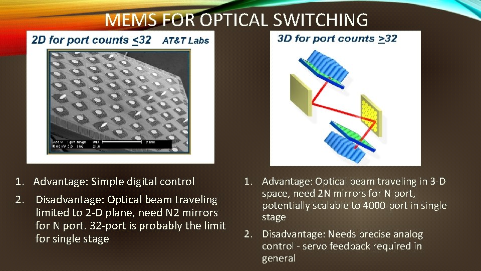
MEMS FOR OPTICAL SWITCHING 1. Advantage: Simple digital control 2. Disadvantage: Optical beam traveling limited to 2 -D plane, need N 2 mirrors for N port. 32 -port is probably the limit for single stage 1. Advantage: Optical beam traveling in 3 -D space, need 2 N mirrors for N port, potentially scalable to 4000 -port in single stage 2. Disadvantage: Needs precise analog control - servo feedback required in general

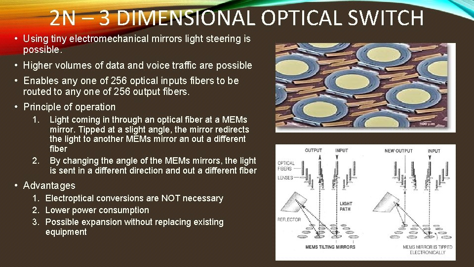
2 N – 3 DIMENSIONAL OPTICAL SWITCH • Using tiny electromechanical mirrors light steering is possible. • Higher volumes of data and voice traffic are possible • Enables any one of 256 optical inputs fibers to be routed to any one of 256 output fibers. • Principle of operation 1. 2. Light coming in through an optical fiber at a MEMs mirror. Tipped at a slight angle, the mirror redirects the light to another MEMs mirror an out a different fiber By changing the angle of the MEMs mirrors, the light is sent in a different direction and out a different fiber • Advantages 1. Electroptical conversions are NOT necessary 2. Lower power consumption 3. Possible expansion without replacing existing equipment