Notes on Diodes 1 Diode saturation current The
- Slides: 22

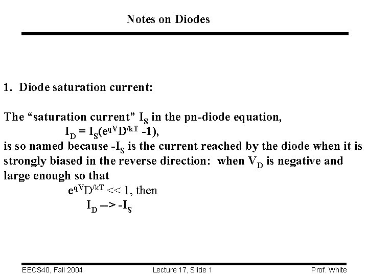
Notes on Diodes 1. Diode saturation current: The “saturation current” IS in the pn-diode equation, ID = IS(eq. VD/k. T -1), is so named because -IS is the current reached by the diode when it is strongly biased in the reverse direction: when VD is negative and large enough so that eq. VD/k. T << 1, then ID --> -IS EECS 40, Fall 2004 Lecture 17, Slide 1 Prof. White

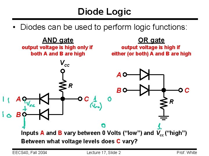
Diode Logic • Diodes can be used to perform logic functions: AND gate OR gate output voltage is high only if both A and B are high output voltage is high if either (or both) A and B are high Vcc A R A B C C R B Inputs A and B vary between 0 Volts (“low”) and Vcc (“high”) Between what voltage levels does C vary? EECS 40, Fall 2004 Lecture 17, Slide 2 Prof. White

Lecture #17 OUTLINE • MOSFET ID vs. VGS characteristic • Circuit models for the MOSFET – resistive switch model – small-signal model Reading • Rabaey et al. : Chapter 3. 3. 2 • Hambley: Chapter 12 (through 12. 5) EECS 40, Fall 2004 Lecture 17, Slide 3 Prof. White

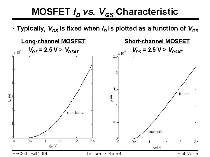
MOSFET ID vs. VGS Characteristic • Typically, VDS is fixed when ID is plotted as a function of VGS Long-channel MOSFET VDS = 2. 5 V > VDSAT EECS 40, Fall 2004 Short-channel MOSFET VDS = 2. 5 V > VDSAT Lecture 17, Slide 4 Prof. White

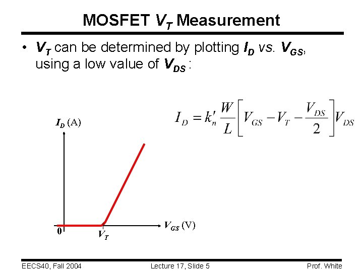
MOSFET VT Measurement • VT can be determined by plotting ID vs. VGS, using a low value of VDS : ID (A) 0 EECS 40, Fall 2004 VT VGS (V) Lecture 17, Slide 5 Prof. White

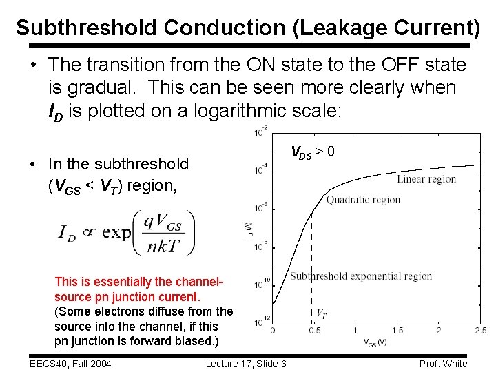
Subthreshold Conduction (Leakage Current) • The transition from the ON state to the OFF state is gradual. This can be seen more clearly when ID is plotted on a logarithmic scale: VDS > 0 • In the subthreshold (VGS < VT) region, This is essentially the channelsource pn junction current. (Some electrons diffuse from the source into the channel, if this pn junction is forward biased. ) EECS 40, Fall 2004 Lecture 17, Slide 6 Prof. White

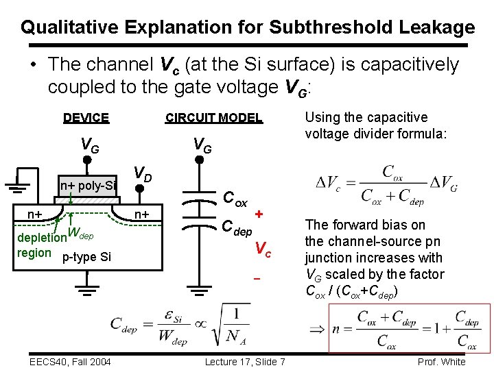
Qualitative Explanation for Subthreshold Leakage • The channel Vc (at the Si surface) is capacitively coupled to the gate voltage VG: DEVICE CIRCUIT MODEL VG n+ poly-Si n+ depletion. Wdep region p-type Si VG VD n+ Cox Cdep + Vc – EECS 40, Fall 2004 Using the capacitive voltage divider formula: Lecture 17, Slide 7 The forward bias on the channel-source pn junction increases with VG scaled by the factor Cox / (Cox+Cdep) Prof. White

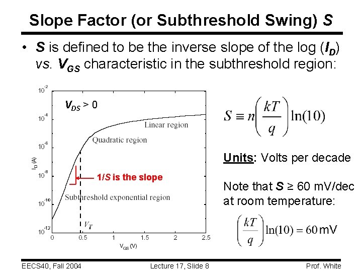
Slope Factor (or Subthreshold Swing) S • S is defined to be the inverse slope of the log (ID) vs. VGS characteristic in the subthreshold region: VDS > 0 Units: Volts per decade 1/S is the slope EECS 40, Fall 2004 Lecture 17, Slide 8 Note that S ≥ 60 m. V/dec at room temperature: Prof. White

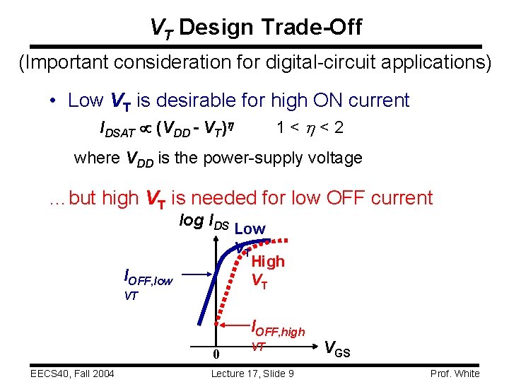
VT Design Trade-Off (Important consideration for digital-circuit applications) • Low VT is desirable for high ON current 1< <2 IDSAT (VDD - VT) where VDD is the power-supply voltage …but high VT is needed for low OFF current log IDS IOFF, low VT Low VT High VT IOFF, high 0 EECS 40, Fall 2004 VT Lecture 17, Slide 9 VGS Prof. White

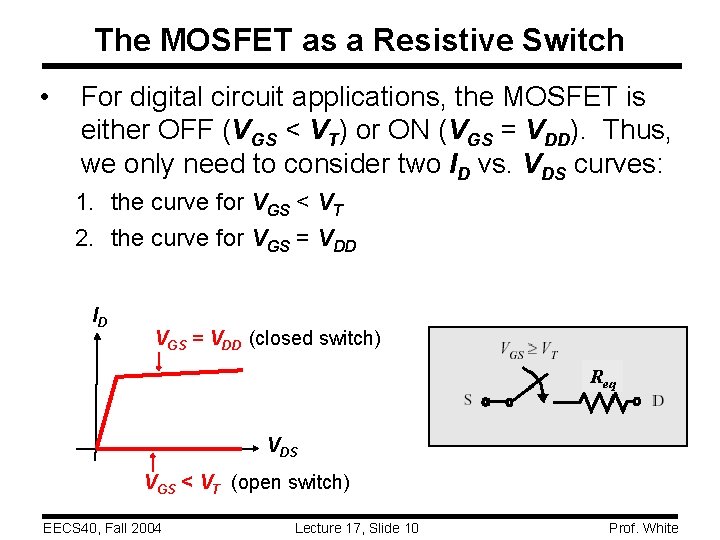
The MOSFET as a Resistive Switch • For digital circuit applications, the MOSFET is either OFF (VGS < VT) or ON (VGS = VDD). Thus, we only need to consider two ID vs. VDS curves: 1. the curve for VGS < VT 2. the curve for VGS = VDD ID VGS = VDD (closed switch) Req VDS VGS < VT (open switch) EECS 40, Fall 2004 Lecture 17, Slide 10 Prof. White

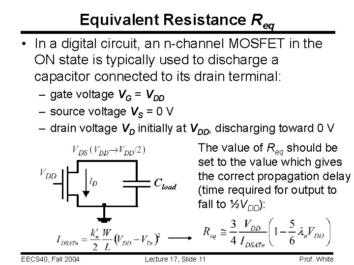
Equivalent Resistance Req • In a digital circuit, an n-channel MOSFET in the ON state is typically used to discharge a capacitor connected to its drain terminal: – gate voltage VG = VDD – source voltage VS = 0 V – drain voltage VD initially at VDD, discharging toward 0 V Cload EECS 40, Fall 2004 The value of Req should be set to the value which gives the correct propagation delay (time required for output to fall to ½VDD): Lecture 17, Slide 11 Prof. White

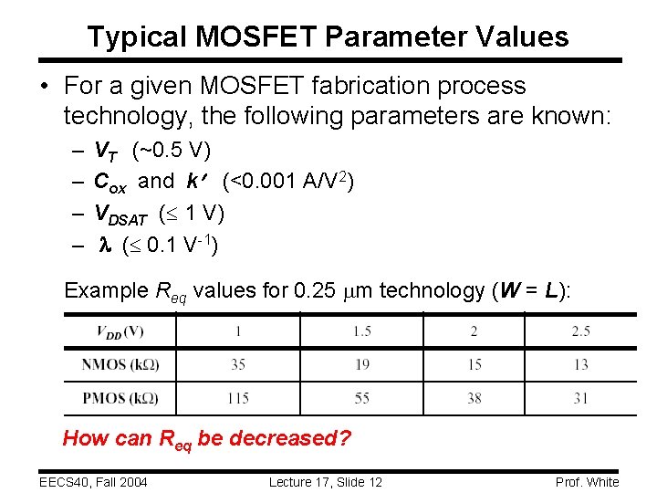
Typical MOSFET Parameter Values • For a given MOSFET fabrication process technology, the following parameters are known: – – VT (~0. 5 V) Cox and k (<0. 001 A/V 2) VDSAT ( 1 V) l ( 0. 1 V-1) Example Req values for 0. 25 mm technology (W = L): How can Req be decreased? EECS 40, Fall 2004 Lecture 17, Slide 12 Prof. White

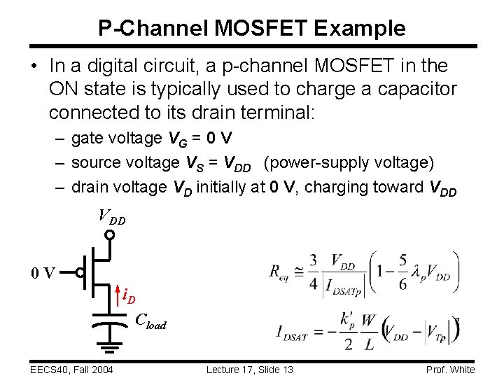
P-Channel MOSFET Example • In a digital circuit, a p-channel MOSFET in the ON state is typically used to charge a capacitor connected to its drain terminal: – gate voltage VG = 0 V – source voltage VS = VDD (power-supply voltage) – drain voltage VD initially at 0 V, charging toward VDD 0 V i. D Cload EECS 40, Fall 2004 Lecture 17, Slide 13 Prof. White

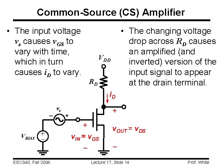
Common-Source (CS) Amplifier • The input voltage vs causes v. GS to vary with time, which in turn causes i. D to vary. • The changing voltage drop across RD causes an amplified (and inverted) version of the input signal to appear at the drain terminal. VDD RD i. D VBIAS + – EECS 40, Fall 2004 vs + + + v. IN = v. GS v. OUT = v. DS Lecture 17, Slide 14 Prof. White

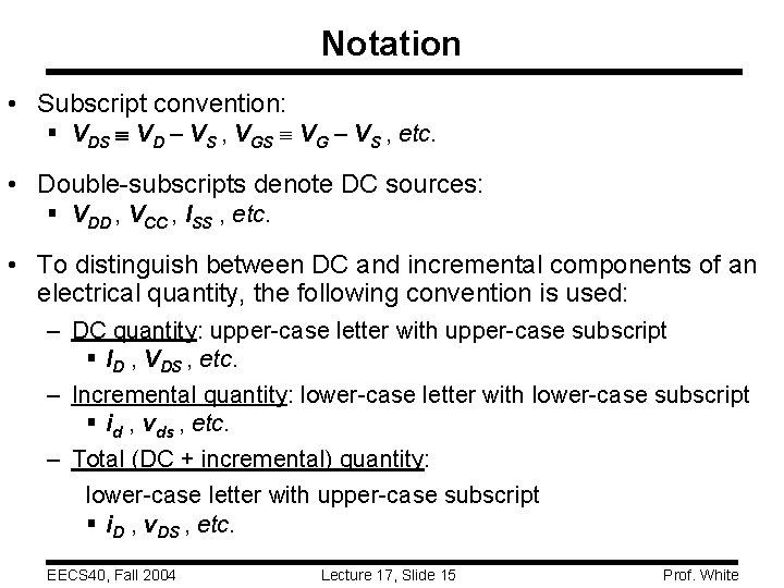
Notation • Subscript convention: § VDS VD – VS , VGS VG – VS , etc. • Double-subscripts denote DC sources: § VDD , VCC , ISS , etc. • To distinguish between DC and incremental components of an electrical quantity, the following convention is used: – DC quantity: upper-case letter with upper-case subscript § ID , VDS , etc. – Incremental quantity: lower-case letter with lower-case subscript § id , vds , etc. – Total (DC + incremental) quantity: lower-case letter with upper-case subscript § i. D , v. DS , etc. EECS 40, Fall 2004 Lecture 17, Slide 15 Prof. White

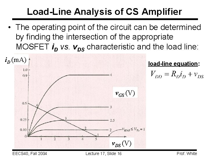
Load-Line Analysis of CS Amplifier • The operating point of the circuit can be determined by finding the intersection of the appropriate MOSFET i. D vs. v. DS characteristic and the load line: i. D (m. A) load-line equation: v. GS (V) v. DS (V) EECS 40, Fall 2004 Lecture 17, Slide 16 Prof. White

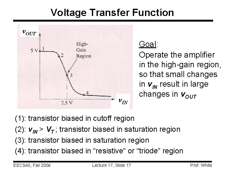
Voltage Transfer Function v. OUT v. IN Goal: Operate the amplifier in the high-gain region, so that small changes in v. IN result in large changes in v. OUT (1): transistor biased in cutoff region (2): v. IN > VT ; transistor biased in saturation region (3): transistor biased in saturation region (4): transistor biased in “resistive” or “triode” region EECS 40, Fall 2004 Lecture 17, Slide 17 Prof. White

Quiescent Operating Point • The operating point of the amplifier for zero input signal (vs = 0) is often referred to as the quiescent operating point. (Another word: bias. ) – The bias point should be chosen so that the output voltage is approximately centered between VDD and 0 V. – vs varies the input voltage around the input bias point. Note: The relationship between v. OUT and v. IN is not linear; this can result in a distorted output voltage signal. If the input signal amplitude is very small, however, we can have amplification with negligible distortion. EECS 40, Fall 2004 Lecture 17, Slide 18 Prof. White

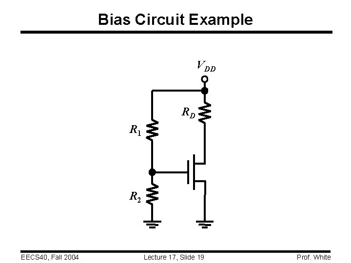
Bias Circuit Example VDD RD R 1 R 2 EECS 40, Fall 2004 Lecture 17, Slide 19 Prof. White

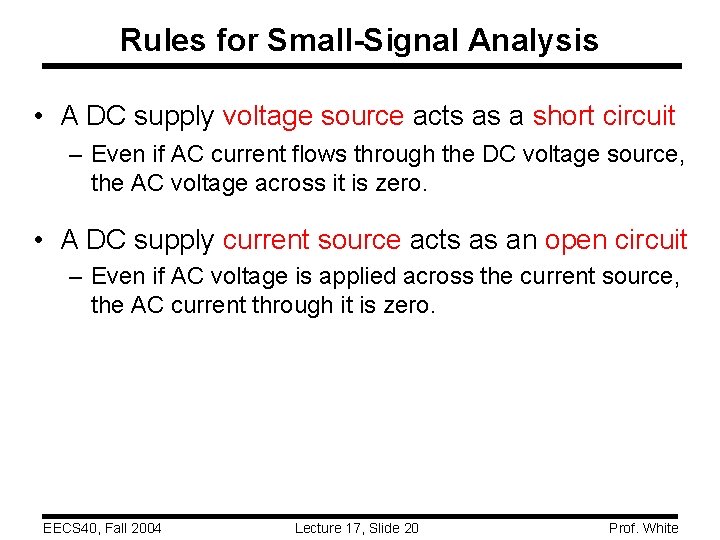
Rules for Small-Signal Analysis • A DC supply voltage source acts as a short circuit – Even if AC current flows through the DC voltage source, the AC voltage across it is zero. • A DC supply current source acts as an open circuit – Even if AC voltage is applied across the current source, the AC current through it is zero. EECS 40, Fall 2004 Lecture 17, Slide 20 Prof. White

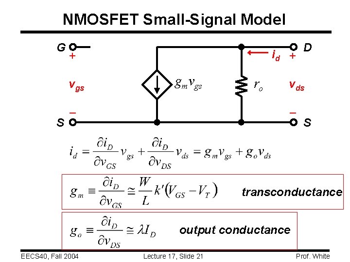
NMOSFET Small-Signal Model G + vgs S id + gmvgs ro D vds S transconductance output conductance EECS 40, Fall 2004 Lecture 17, Slide 21 Prof. White

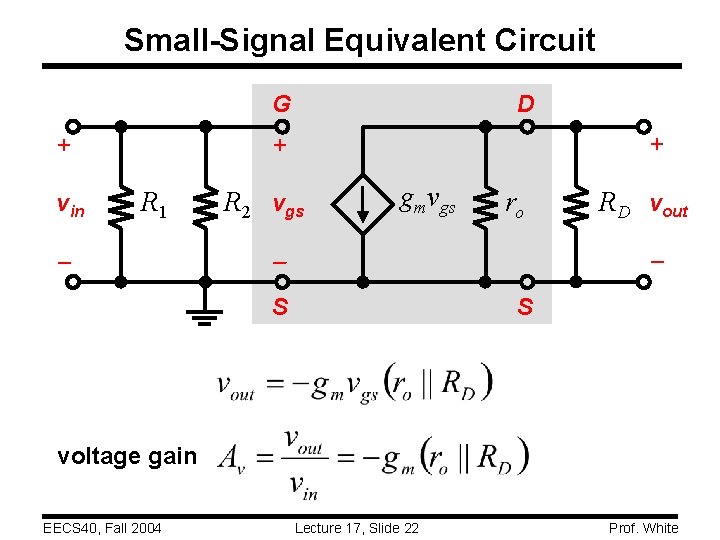
Small-Signal Equivalent Circuit G + vin D + + R 1 R 2 vgs gmvgs ro RD vout S S voltage gain EECS 40, Fall 2004 Lecture 17, Slide 22 Prof. White