PN Junction Physical and Mathematical Description of Operation


 Equilibrium analysis of step junctions (a) Built-in voltage Vbi: p-side n-side + q.")
 Depletion region width: Solve 1 D Poisson equation using depletion charge approximation, subject")
 Maximum electric field: The maximum electric field, which occurs at the metallurgical junction,")
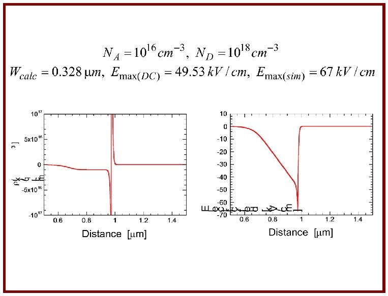
 Analytical vs. numerical data")
 Depletion layer capacitance: Consider a p+n, or one-sided junction, for which: The depletion")
 Equilibrium analysis of linearly-graded junction: (a) Depletion layer width: (c) Maximum electric field:")
 Ideal Current-Voltage Characteristics: Assumptions: • Abrupt depletion layer approximation • Low-level injection injected")
 Quasi-neutral regions: • Using minority carrier continuity equations, one arrives at the following")

 Total current density: • Total current equals the sum of the minority carrier")
 Origin of the current flow: Forward bias: Reverse bias: Ln Lp Reverse saturation")
 Majority carriers current: • Consider a forward-biased diode under low-level injection conditions: Quasi-neutrality")

 Limitations of the Shockley model: • The simplified Shockley model accurately describes IVcharacteristics")
 Generation and Recombination Currents Continuity equation for holes: Steady-state and no light genera-")


 Breakdown Mechanisms • Junction breakdown can be due to: tunneling breakdown avalanche breakdown")

: Reverse-bias band diagram: EFp EFn")


 an=ap (semiconductor with equal ionization rates): (b) an>>ap (impact")
 Step p+n-junction • For one sided junction we can make the")
 Step p+-n-n+ junction • Extension of the n-layer large: • Extension of the")

 Plane vs. planar or cylindrical junction • Plane junction: Maximum electric field: p+")
 AC-Analysis and Diode Switching (a) Diffusion capacitance and small-signal equivalent circuit • This")
: • Boundary conditions: • Final expression for pn")


 Diode switching • For switching applications, the transition from forward bias to reverse")


- Slides: 45
PN Junction: Physical and Mathematical Description of Operation Dragica Vasileska Professor Arizona State University • • • PN Junctions – General Considerations Ideal Current-Voltage Characteristics Generation and Recombination Currents Breakdown Mechanisms AC-Analysis and Diode Switching
1. PN-junctions - General Consideration: • PN-junction is a two terminal device. • Based on the doping profile, PN-junctions can be separated into two major categories: - step junctions - linearly-graded junctions n-side p-side Step junction p-side n-side Linearly-graded junction
(A) Equilibrium analysis of step junctions (a) Built-in voltage Vbi: p-side n-side + q. ND -q. NA - (b) Majority- minority carrier relationship:
(c) Depletion region width: Solve 1 D Poisson equation using depletion charge approximation, subject to the following boundary conditions: p-side: n-side: Use the continuity of the two solutions at x=0, and charge neutrality, to obtain the expression for the depletion region width W:
(d) Maximum electric field: The maximum electric field, which occurs at the metallurgical junction, is given by: (e) Carrier concentration variation:
(f) Analytical vs. numerical data
(g) Depletion layer capacitance: Consider a p+n, or one-sided junction, for which: The depletion layer capacitance is calculated using: Measurement setup: W Reverse bias Forward bias vac ~ V d. W
(B) Equilibrium analysis of linearly-graded junction: (a) Depletion layer width: (c) Maximum electric field: (d) Depletion layer capacitance: Based on accurate numerical simulations, the depletion layer capacitance can be more accurately calculated if Vbi is replaced by the gradient voltage Vg:
(2) Ideal Current-Voltage Characteristics: Assumptions: • Abrupt depletion layer approximation • Low-level injection injected minority carrier density much smaller than the majority carrier density • No generation-recombination within the space-charge region (SCR) (a) Depletion layer:
(b) Quasi-neutral regions: • Using minority carrier continuity equations, one arrives at the following expressions for the excess hole and electron densities in the quasi-neutral regions: Space-charge region W Forward bias Reverse bias
• Corresponding minority-carriers diffusion current densities are: Shockley model No SCR generation/recombination
(c) Total current density: • Total current equals the sum of the minority carrier diffusion currents defined at the edges of the SCR: I Ge Si Ga. As V • Reverse saturation current IS:
(d) Origin of the current flow: Forward bias: Reverse bias: Ln Lp Reverse saturation current is due to minority carriers being collected over a distance on the order of the diffusion length.
(e) Majority carriers current: • Consider a forward-biased diode under low-level injection conditions: Quasi-neutrality requires: This leads to: • Total hole current in the quasi-neutral regions:
• Electron drift current in the quasi-neutral region:
(f) Limitations of the Shockley model: • The simplified Shockley model accurately describes IVcharacteristics of Ge diodes at low current densities. • For Si and Ge diodes, one needs to take into account several important non-ideal effects, such as: Generation and recombination of carriers within the depletion region. Series resistance effects due to voltage drop in the quasi -neutral regions. Junction breakdown at large reverse biases due to tun- neling and impact ionization effects.
(3) Generation and Recombination Currents Continuity equation for holes: Steady-state and no light genera- tion process: • Space-charge region recombination current:
Reverse-bias conditions: • Concentrations n and p are negligible in the depletion region: Generation lifetime • Space-charge region current is actually generation current: • Total reverse-saturation current:
• Generation current dominates when ni is small, which is always the case for Si and Ga. As diodes. I (log-scale) V (log-scale) W IV-characteristics under reverse bias conditions Generated carriers are swept away from the depletion region.
Forward-bias conditions: • Concentrations n and p are large in the depletion region: • Condition for maximum recombination rate: Recombination lifetime • Estimate of the recombination current:
• Exact expression for the recombination current: • Corrections to the model: • Total forward current: ideality factor. Deviations of from unity represent an important measure for the recombination current.
• Importance of recombination effects: Low voltages, small ni recombination current dominates Large voltages diffusion current dominates log(I) V
(4) Breakdown Mechanisms • Junction breakdown can be due to: tunneling breakdown avalanche breakdown • One can determine which mechanism is responsible for the breakdown based on the value of the breakdown voltage VBD : VBD < 4 Eg/q tunneling breakdown VBD > 6 Eg/q avalanche breakdown 4 Eg/q < VBD < 6 Eg/q both tunneling and avalanche mechanisms are responsible
Tunneling breakdown: • Tunneling breakdown occurs in heavily-doped pnjunctions in which the depletion region width W is about 10 nm. Zero-bias band diagram: EF EC W EV Forward-bias band diagram: EFn EFp EC EV W
• Tunneling current (obtained by using WKB approximation): Reverse-bias band diagram: EFp EFn EC Fcr average electric field in the junction • The critical voltage for tunneling breakdown, VBR, is estimated from: EV • With T , Eg and It .
Avalanche breakdown: • Most important mechanism in junction breakdown, i. e. it imposes an upper limit on the reverse bias for most diodes. • Impact ionization is characterized by ionization rates an and ap, defined as probabilities for impact ionization per unit length, i. e. how many electron-hole pairs have been generated per particle per unit length: - Ei critical energy for impact ionization to occur - Fcr critical electric field - l mean-free path for carriers
Avalanche mechanism: EFp EFn EC EV Generation of the excess electron-hole pairs is due to impact ionization. Expanded view of the depletion region
• Description of the avalanche process: dx Impact ionization initiated by electrons. dx Impact ionization initiated by holes. Multiplication factors for electrons and holes:
• Breakdown voltage for which the multiplication rates Mn and Mp become infinite. For this purpose, one needs to express Mn and Mp in terms of an and ap: The breakdown condition does not depend on which type of carrier initiated the process.
• Limiting cases: (a) an=ap (semiconductor with equal ionization rates): (b) an>>ap (impact ionization dominated by one carrier):
Breakdown voltages: (a) Step p+n-junction • For one sided junction we can make the following approximation: • Voltage drop across the depletion region on the n-side: • Maximum electric field: • Empirical expression for the breakdown voltage VBD:
(b) Step p+-n-n+ junction • Extension of the n-layer large: • Extension of the n-layer small: • Final expression for the punchthrough voltage VP:
• Doping-dependence of the breakdown voltage VBD: Width of the n-layer W 1 increases Log-scale One-sided abrupt junction Tunneling breakdown p+-n-n+ Log-scale • Temperature dependence: As temperature increases, lattice scattering increases which makes impact ionization less probable. As a result of this, the breakdown voltage increases.
(c) Plane vs. planar or cylindrical junction • Plane junction: Maximum electric field: p+ n • Planar junction: Except for surface effects, this is an ideal junction. Maximum electric field: rj p+ W n The smaller the radius rj, the larger the electric field crowding.
(5) AC-Analysis and Diode Switching (a) Diffusion capacitance and small-signal equivalent circuit • This is capacitance related to the change of the minority carriers. It is important (even becomes dominant) under forward bias conditions. • The diffusion capacitance is obtained from the device impedance, and using the continuity equation for minority carriers: • Applied voltages, currents and solution for Dpn:
• Equation for pn 1(x): • Boundary conditions: • Final expression for pn 1(x):
• Small-signal hole current: • Low-frequency limit for the admittance Y: • RC-constant: The characteristic time constant is on the order of the minority carriers lifetime.
• Equivalent circuit model forward bias: • Bias dependence:
(b) Diode switching • For switching applications, the transition from forward bias to reverse bias must be nearly abrupt and the transit time short. • Diode turn-on and turn-off characteristics can be obtained from the solution of the continuity equations: Qp(t) = excess hole charge Valid for p+n diode
Diode turn-on: • For t<0, the switch is open, and the excess hole charge is: p+ t=0 • At t=0, the switch closes, and we have the following boundary condition: IF • Final expression for the excess hole charge: n
• Graphical representation: Slope almost constant t increasing • Steady state value for the bias across the diode:
Diode turn-off: • For t<0, the switch is in position 1, and a steady-state situation is established: • At t=0, the switch is moved to position 2, and up until time t=t 1 we have: • The current through the diode until time t 1 is: p+ t=0 VF 1 R 2 VR R n
• To solve exactly this problem and find diode switching time, is a rather difficult task. To simplify the problem, we make the crucial assumption that IR remains constant even beyond t 1. • The differential equation to be solved and the initial condition are, thus, of the form: • This gives the following final solution: • Diode switching time:
• Graphical representation: Slope almost constant t=0 t=ts t trr ts switching time trr reverse recovery time