ECE 340 Lecture 23 Current Flow in PN
- Slides: 18

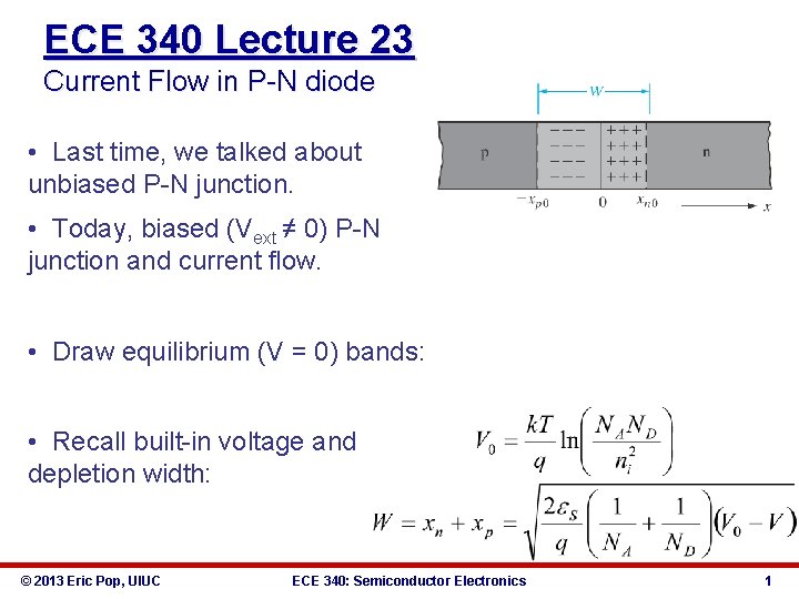
ECE 340 Lecture 23 Current Flow in P-N diode • Last time, we talked about unbiased P-N junction. • Today, biased (Vext ≠ 0) P-N junction and current flow. • Draw equilibrium (V = 0) bands: • Recall built-in voltage and depletion width: © 2013 Eric Pop, UIUC ECE 340: Semiconductor Electronics 1

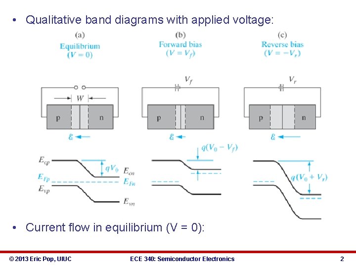
• Qualitative band diagrams with applied voltage: • Current flow in equilibrium (V = 0): © 2013 Eric Pop, UIUC ECE 340: Semiconductor Electronics 2

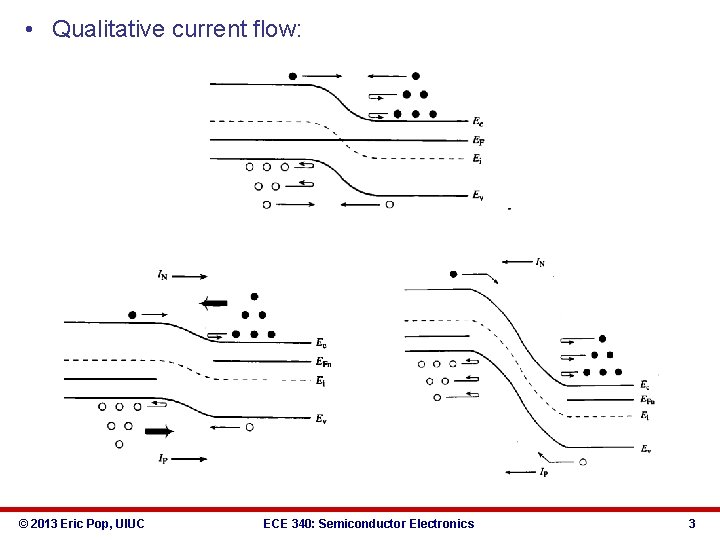
• Qualitative current flow: © 2013 Eric Pop, UIUC ECE 340: Semiconductor Electronics 3

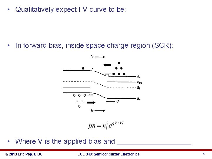
• Qualitatively expect I-V curve to be: • In forward bias, inside space charge region (SCR): • Where V is the applied bias and __________ © 2013 Eric Pop, UIUC ECE 340: Semiconductor Electronics 4

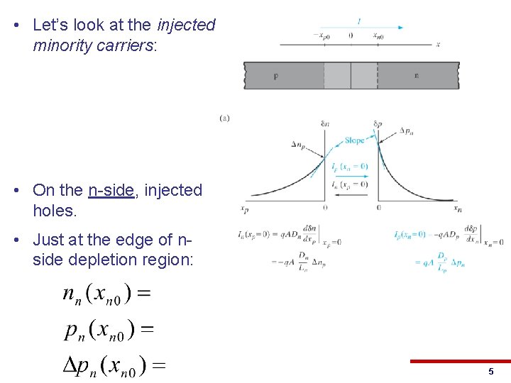
• Let’s look at the injected minority carriers: • On the n-side, injected holes. • Just at the edge of nside depletion region: © 2013 Eric Pop, UIUC ECE 340: Semiconductor Electronics 5

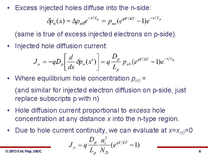
• Excess injected holes diffuse into the n-side: (same is true of excess injected electrons on p-side). • Injected hole diffusion current: • Where equilibrium hole concentration pn 0 = (and similar for injected electron diffusion on p-side, just replace subscripts p with n) • Hole diffusion current proportional to excess hole concentration at any distance x into the n-type region. • Due to hole current continuity, we can evaluate at x=xn 0=0 © 2013 Eric Pop, UIUC ECE 340: Semiconductor Electronics 6

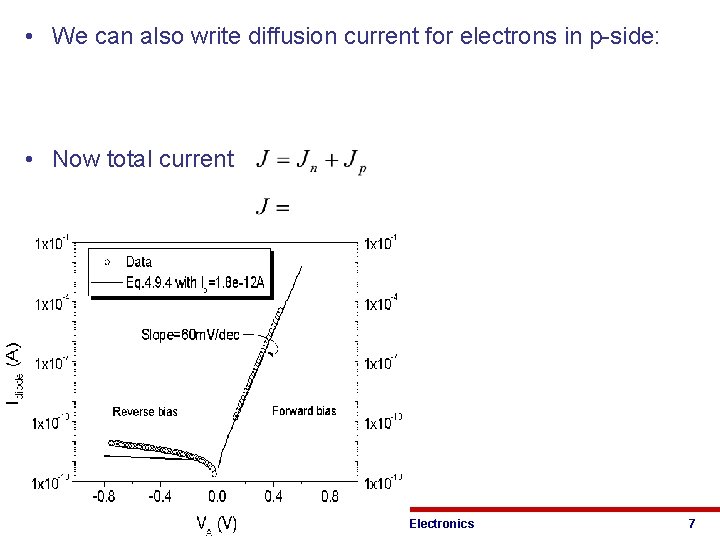
• We can also write diffusion current for electrons in p-side: • Now total current © 2013 Eric Pop, UIUC ECE 340: Semiconductor Electronics 7

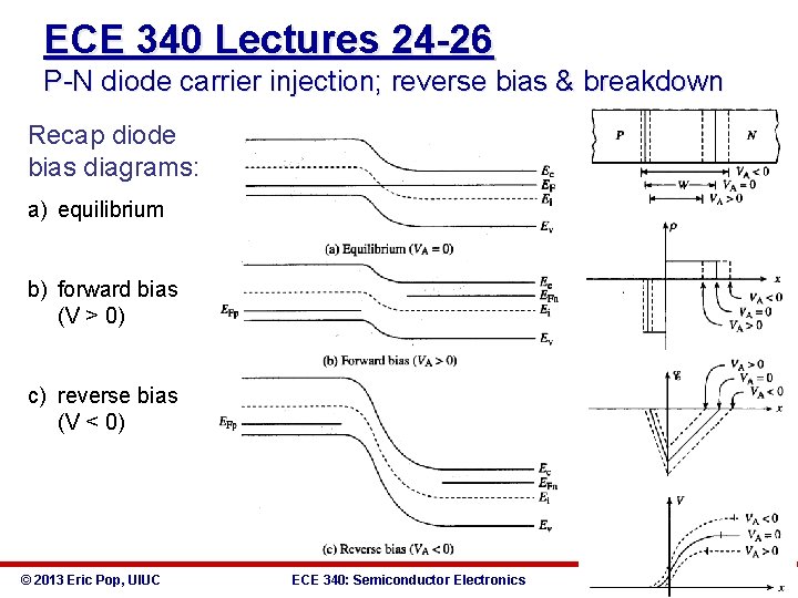
ECE 340 Lectures 24 -26 P-N diode carrier injection; reverse bias & breakdown Recap diode bias diagrams: a) equilibrium b) forward bias (V > 0) c) reverse bias (V < 0) © 2013 Eric Pop, UIUC ECE 340: Semiconductor Electronics 8

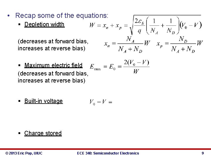
• Recap some of the equations: § Depletion width (decreases at forward bias, increases at reverse bias) § Maximum electric field (decreases at forward bias, increases at reverse bias) § Built-in voltage § Charge stored © 2013 Eric Pop, UIUC ECE 340: Semiconductor Electronics 9

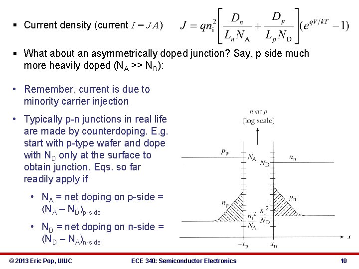
§ Current density (current I = J∙A) § What about an asymmetrically doped junction? Say, p side much more heavily doped (NA >> ND): • Remember, current is due to minority carrier injection • Typically p-n junctions in real life are made by counterdoping. E. g. start with p-type wafer and dope with ND only at the surface to obtain junction. Eqs. so far readily apply if • NA = net doping on p-side = (NA – ND)p-side • ND = net doping on n-side = (ND – NA)n-side © 2013 Eric Pop, UIUC ECE 340: Semiconductor Electronics 10

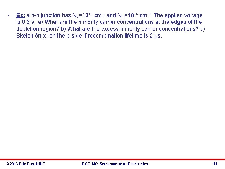
• Ex: a p-n junction has NA=1019 cm-3 and ND=1016 cm-3. The applied voltage is 0. 6 V. a) What are the minority carrier concentrations at the edges of the depletion region? b) What are the excess minority carrier concentrations? c) Sketch δn(x) on the p-side if recombination lifetime is 2 μs. © 2013 Eric Pop, UIUC ECE 340: Semiconductor Electronics 11

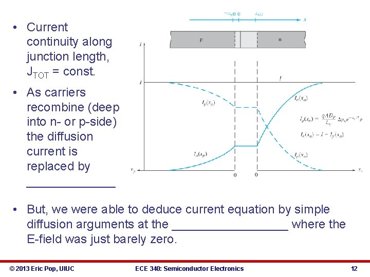
• Current continuity along junction length, JTOT = const. • As carriers recombine (deep into n- or p-side) the diffusion current is replaced by _______ • But, we were able to deduce current equation by simple diffusion arguments at the _________ where the E-field was just barely zero. © 2013 Eric Pop, UIUC ECE 340: Semiconductor Electronics 12

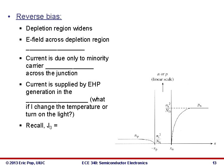
• Reverse bias: § Depletion region widens § E-field across depletion region _________ § Current is due only to minority carrier _______ across the junction § Current is supplied by EHP generation in the _________ (what if I change the temperature or turn on the light? ) § Recall, J 0 = © 2013 Eric Pop, UIUC ECE 340: Semiconductor Electronics 13

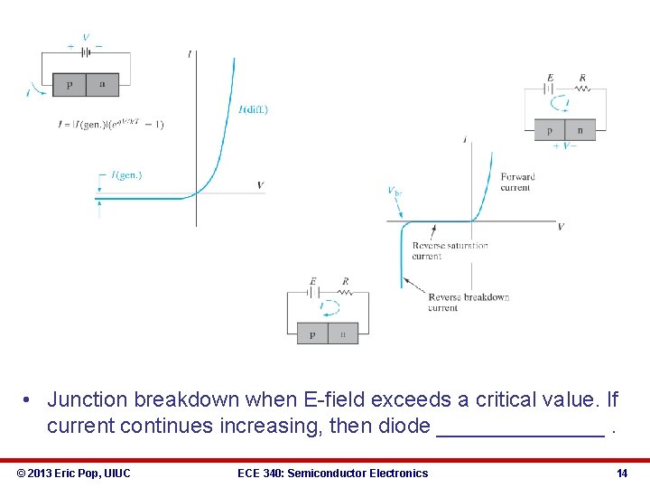
• Junction breakdown when E-field exceeds a critical value. If current continues increasing, then diode _______. © 2013 Eric Pop, UIUC ECE 340: Semiconductor Electronics 14

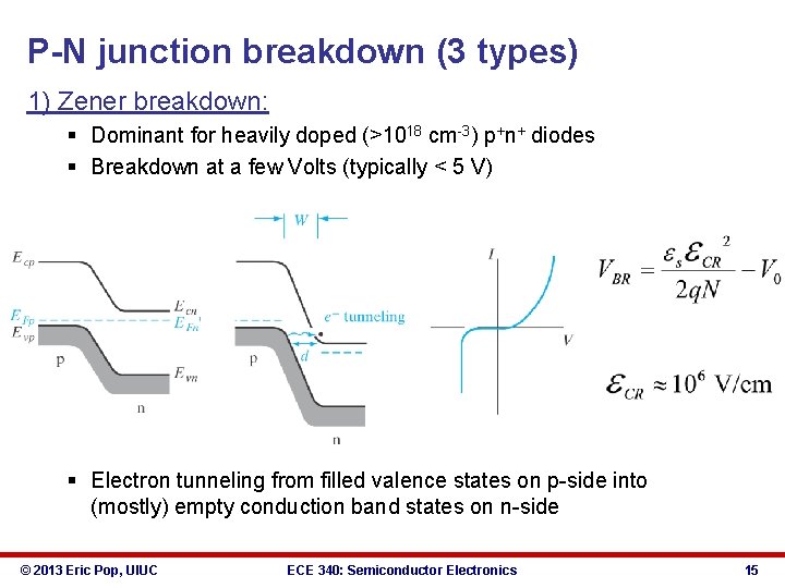
P-N junction breakdown (3 types) 1) Zener breakdown: § Dominant for heavily doped (>1018 cm-3) p+n+ diodes § Breakdown at a few Volts (typically < 5 V) § Electron tunneling from filled valence states on p-side into (mostly) empty conduction band states on n-side © 2013 Eric Pop, UIUC ECE 340: Semiconductor Electronics 15

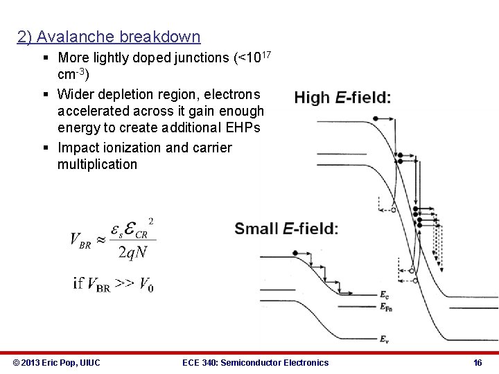
2) Avalanche breakdown § More lightly doped junctions (<1017 cm-3) § Wider depletion region, electrons accelerated across it gain enough energy to create additional EHPs § Impact ionization and carrier multiplication © 2013 Eric Pop, UIUC ECE 340: Semiconductor Electronics 16

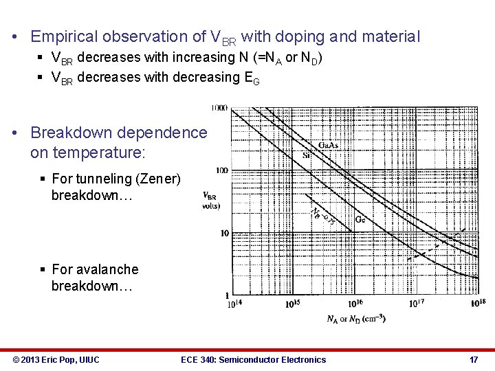
• Empirical observation of VBR with doping and material § VBR decreases with increasing N (=NA or ND) § VBR decreases with decreasing EG • Breakdown dependence on temperature: § For tunneling (Zener) breakdown… § For avalanche breakdown… © 2013 Eric Pop, UIUC ECE 340: Semiconductor Electronics 17

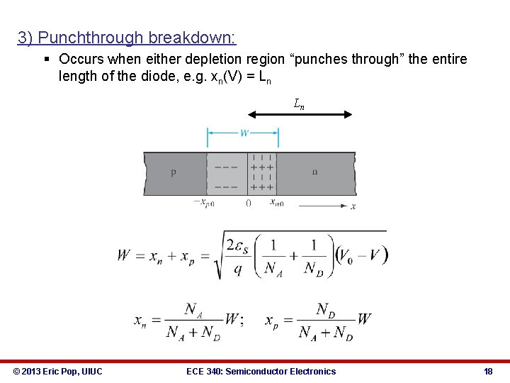
3) Punchthrough breakdown: § Occurs when either depletion region “punches through” the entire length of the diode, e. g. xn(V) = Ln Ln © 2013 Eric Pop, UIUC ECE 340: Semiconductor Electronics 18