Unit2 JUNCTION DIODE CHARACTERISTICS Review of semi conductor
- Slides: 55

Unit-2 JUNCTION DIODE CHARACTERISTICS: Review of semi conductor Physics – n and p –type semi conductors, Mass Action Law, Continuity Equation, Hall Effect, Open-circuited p-n junction, The p-n junction as a rectifier (forward bias and reverse bias), The current components in p-n diode, Law of junction, Diode equation, Energy band diagram of p-n diode, Volt-ampere characteristics of p-n diode, Temperature dependence of VI characteristic, Transition and Diffusion capacitances, Breakdown Mechanisms in Semi Conductor Diodes, Zener diode characteristics, Characteristics of Tunnel Diode, Varactor Diode , LED, LCD. And photo diode.

Atomic Structure An atom is composed of : • Nucleus ( which contains positively charged protons and neutral neutrons) • Electrons (which are negatively charged and that orbit the nucleus)

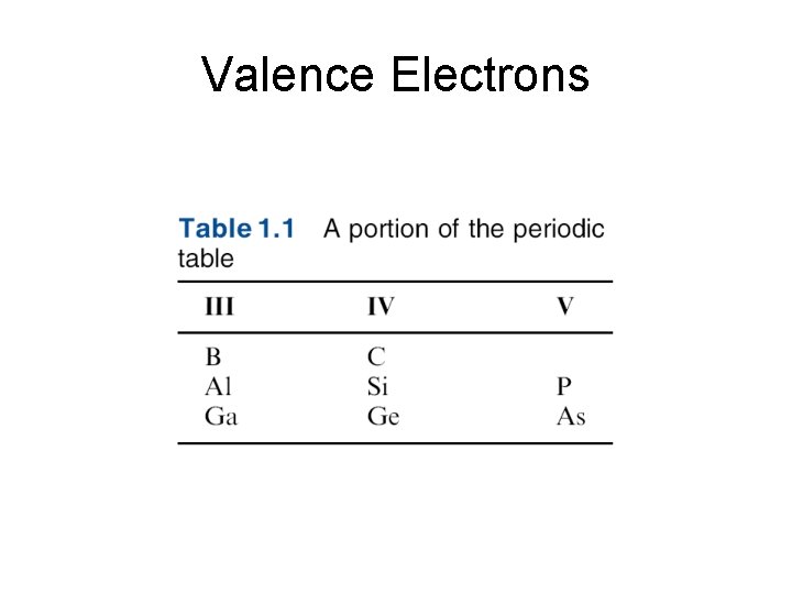
Valence Electrons • Electrons are distributed in various shells at different distances from nucleus • Electron energy increases as shell radius increases. • Electrons in the outermost shell are called valence electrons • Elements in the period table are grouped according to the number of valence electrons

Valence Electrons

Elemental/Compound Semiconductor • Silicon (Si) and Germanium (Ge) are in group IV, and are elemental semiconductors • Galium arsenide (Ga. As) is a goup III-V compound semiconductor

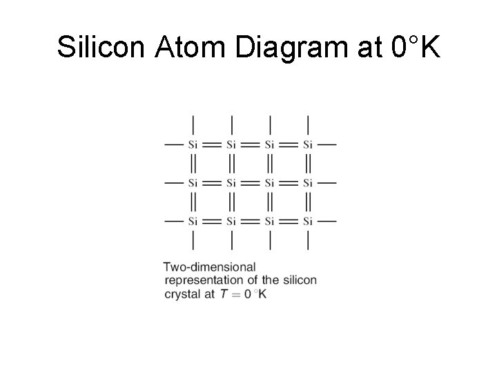
Silicon Crystal • → At 0°K, each electron is in its lowest possible energy state, and each covalent bounding position is filled. • →If a small electric field is applied, the electrons will not move → silicon is an insulator

Silicon Atom Diagram at 0°K

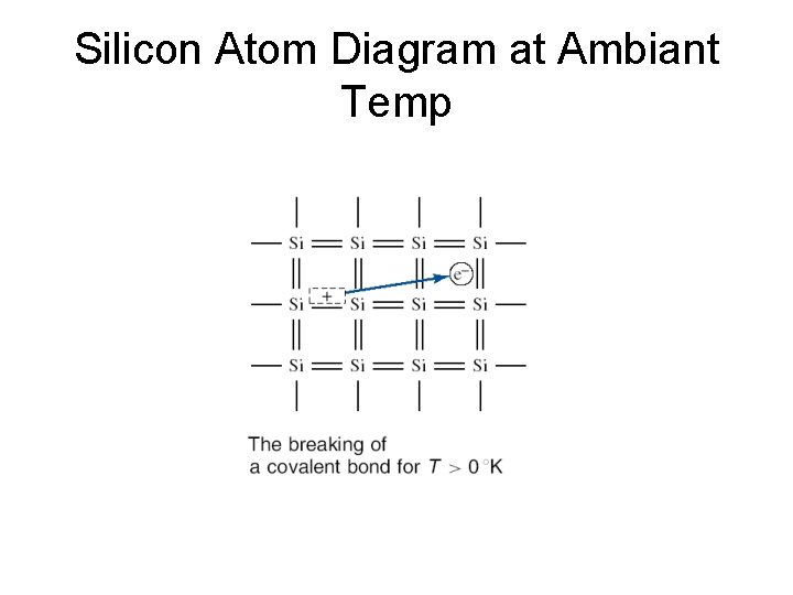
Intrinsic Silicon • → If the temperature increases, the valence electrons will gain some thermal energy, and breaks free from the covalent bond → It leaves a positively charged hole • → In order to break from the covalent bond, a valence electron must gain a minimun energy Eg: Bandgap energy

Silicon Atom Diagram at Ambiant Temp

Insulators/Conductors • Materials that have large bandgap energies (in the range of 3 to 6 electronvolts (e. V)) are insulators, because at room temperature, essentially no free electron exists in the material • Materials that contain very large number of free electrons at room temperature are conductors

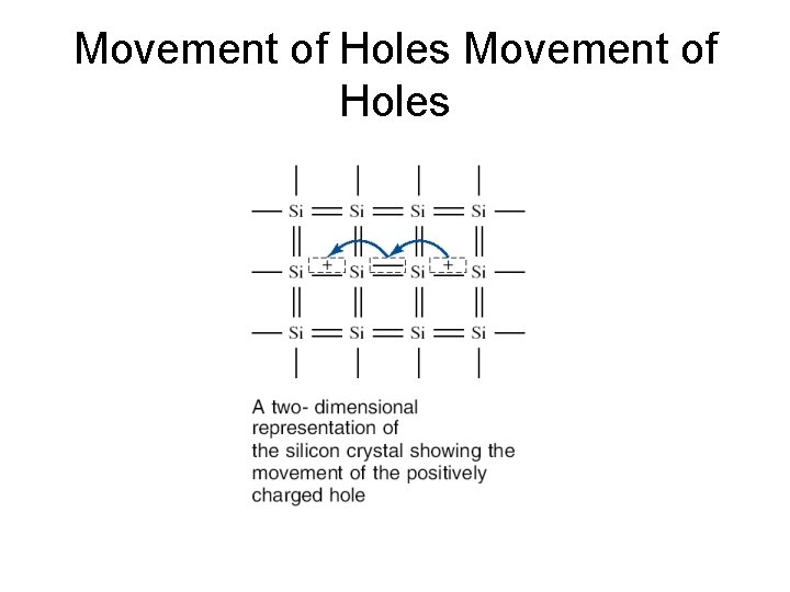
Semiconductors • → In a semiconductor, the bandgap energy is in the order of 1 e. V. The net flow of free electrons causes a current. • → In a semiconductor, two types of charged particles contribute to the current: the negatively charged electrons and the positively charged holes

Movement of Holes

Semiconductor Constants • The concentration of electrons and holes directly influence the magnitde of the current • In an intrinsic semiconductor (a single crystal semiconductor) the densities of holes and electrons are equal.

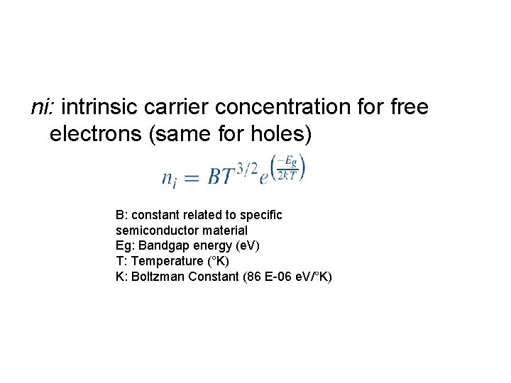
ni: intrinsic carrier concentration for free electrons (same for holes) B: constant related to specific semiconductor material Eg: Bandgap energy (e. V) T: Temperature (°K) K: Boltzman Constant (86 E-06 e. V/°K)

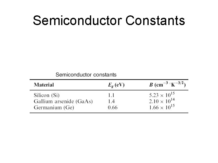
Semiconductor Constants

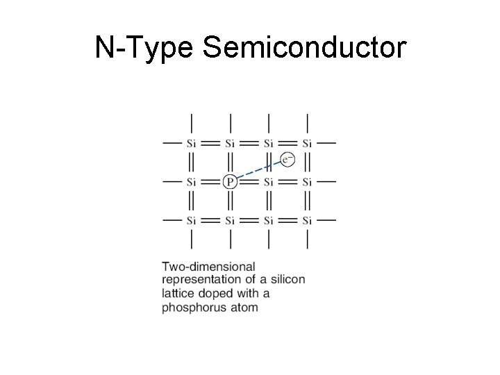
Extrinsic Semiconductor / Doping • The electron or hole concentration can be greatly increased by adding controlled amounts of certain impurities • For silicon, it is desirable to use impurities from the group III and V. • An N-type semiconductor can be created by adding phosphorus or arsenic

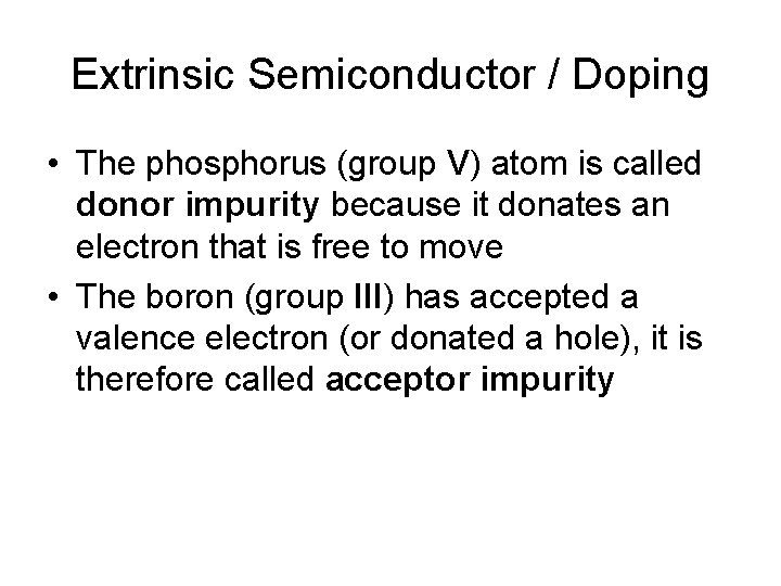
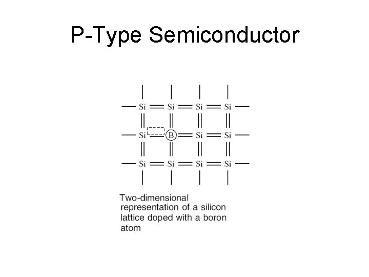
Extrinsic Semiconductor / Doping • The phosphorus (group V) atom is called donor impurity because it donates an electron that is free to move • The boron (group III) has accepted a valence electron (or donated a hole), it is therefore called acceptor impurity

N-Type Semiconductor

P-Type Semiconductor

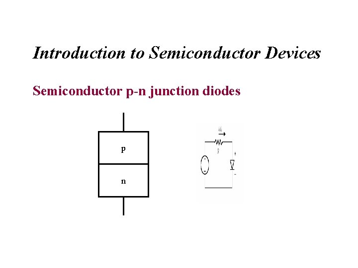
Introduction to Semiconductor Devices Semiconductor p-n junction diodes p n

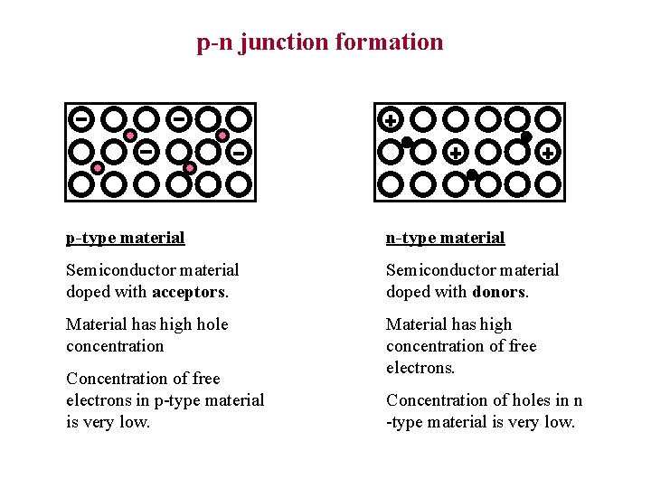
p-n junction formation p-type material n-type material Semiconductor material doped with acceptors. Semiconductor material doped with donors. Material has high hole concentration Material has high concentration of free electrons. Concentration of free electrons in p-type material is very low. Concentration of holes in n -type material is very low.

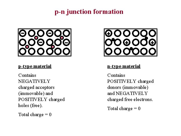
p-n junction formation p-type material n-type material Contains NEGATIVELY charged acceptors (immovable) and POSITIVELY charged holes (free). Contains POSITIVELY charged donors (immovable) and NEGATIVELY charged free electrons. Total charge = 0

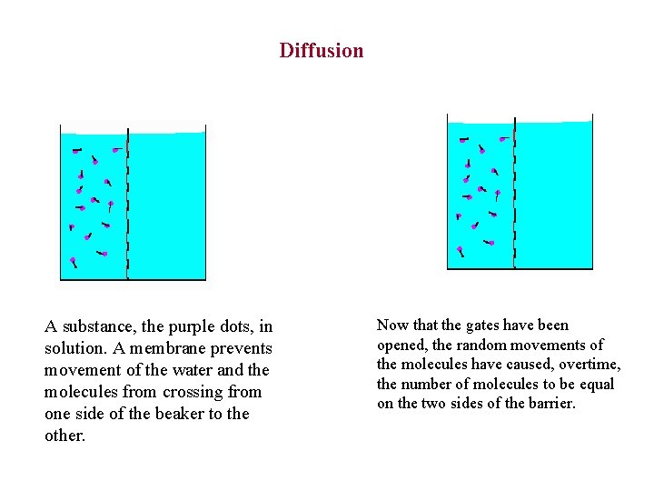
Diffusion A substance, the purple dots, in solution. A membrane prevents movement of the water and the molecules from crossing from one side of the beaker to the other. Now that the gates have been opened, the random movements of the molecules have caused, overtime, the number of molecules to be equal on the two sides of the barrier.

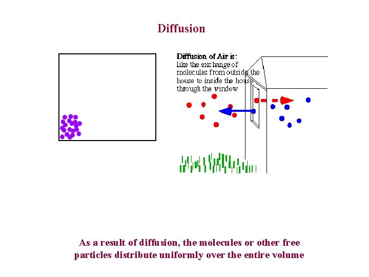
Diffusion As a result of diffusion, the molecules or other free particles distribute uniformly over the entire volume

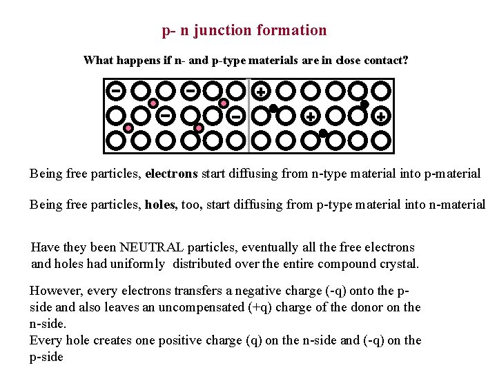
p- n junction formation What happens if n- and p-type materials are in close contact? Being free particles, electrons start diffusing from n-type material into p-material Being free particles, holes, too, start diffusing from p-type material into n-material Have they been NEUTRAL particles, eventually all the free electrons and holes had uniformly distributed over the entire compound crystal. However, every electrons transfers a negative charge (-q) onto the pside and also leaves an uncompensated (+q) charge of the donor on the n-side. Every hole creates one positive charge (q) on the n-side and (-q) on the p-side

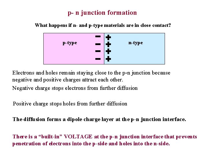
p- n junction formation What happens if n- and p-type materials are in close contact? p-type n-type Electrons and holes remain staying close to the p-n junction because negative and positive charges attract each other. Negative charge stops electrons from further diffusion Positive charge stops holes from further diffusion The diffusion forms a dipole charge layer at the p-n junction interface. There is a “built-in” VOLTAGE at the p-n junction interface that prevents penetration of electrons into the p-side and holes into the n-side.

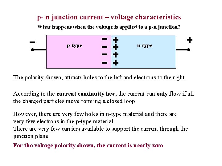
p- n junction current – voltage characteristics What happens when the voltage is applied to a p-n junction? p-type n-type The polarity shown, attracts holes to the left and electrons to the right. According to the current continuity law, the current can only flow if all the charged particles move forming a closed loop However, there are very few holes in n-type material and there are very few electrons in the p-type material. There are very few carriers available to support the current through the junction plane For the voltage polarity shown, the current is nearly zero

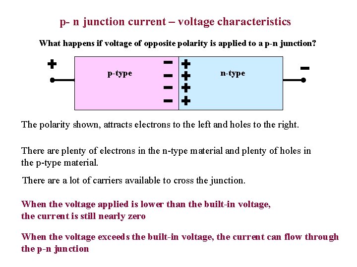
p- n junction current – voltage characteristics What happens if voltage of opposite polarity is applied to a p-n junction? p-type n-type The polarity shown, attracts electrons to the left and holes to the right. There are plenty of electrons in the n-type material and plenty of holes in the p-type material. There a lot of carriers available to cross the junction. When the voltage applied is lower than the built-in voltage, the current is still nearly zero When the voltage exceeds the built-in voltage, the current can flow through the p-n junction

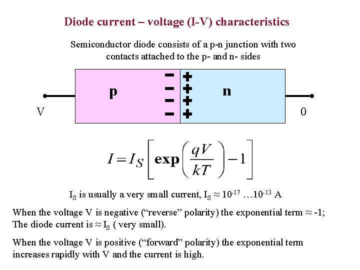
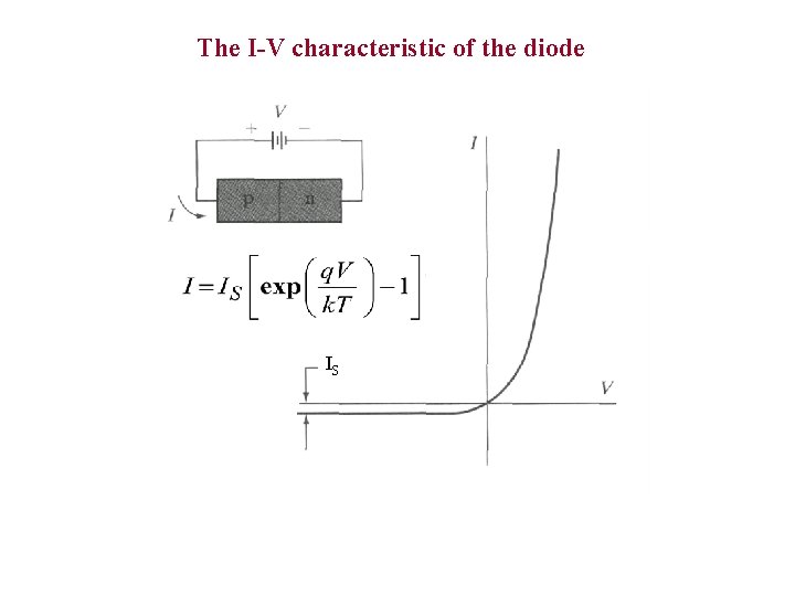
Diode current – voltage (I-V) characteristics Semiconductor diode consists of a p-n junction with two contacts attached to the p- and n- sides p n V 0 IS is usually a very small current, IS ≈ 10 -17 … 10 -13 A When the voltage V is negative (“reverse” polarity) the exponential term ≈ -1; The diode current is ≈ IS ( very small). When the voltage V is positive (“forward” polarity) the exponential term increases rapidly with V and the current is high.

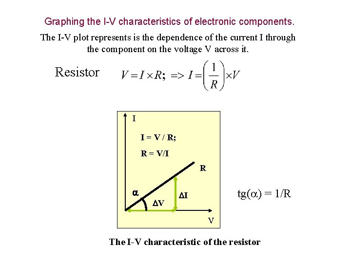
Graphing the I-V characteristics of electronic components. The I-V plot represents is the dependence of the current I through the component on the voltage V across it. Resistor I I = V / R; R = V/I R a DV tg(a) = 1/R DI V The I-V characteristic of the resistor

The I-V characteristic of the diode IS

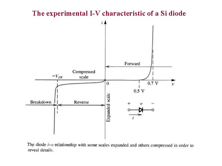
The experimental I-V characteristic of a Si diode

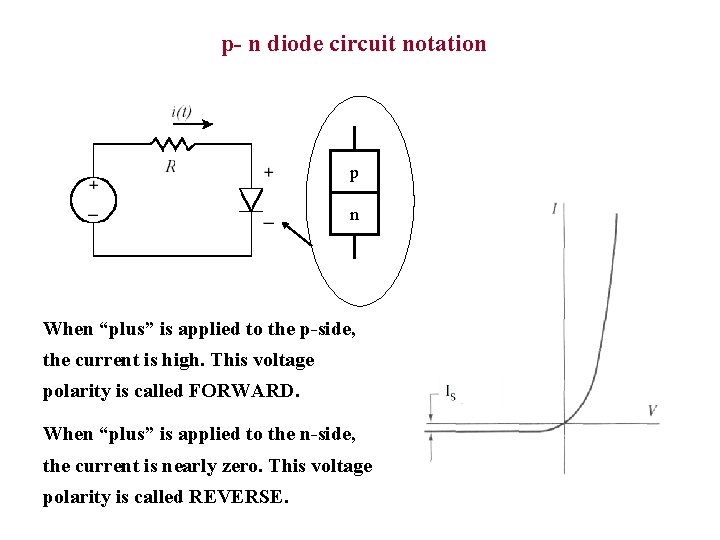
p- n diode circuit notation p n When “plus” is applied to the p-side, the current is high. This voltage polarity is called FORWARD. When “plus” is applied to the n-side, the current is nearly zero. This voltage polarity is called REVERSE.

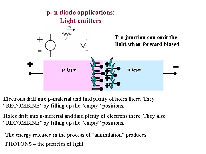
p- n diode applications: Light emitters P-n junction can emit the light when forward biased p-type n-type Electrons drift into p-material and find plenty of holes there. They “RECOMBINE” by filling up the “empty” positions. Holes drift into n-material and find plenty of electrons there. They also “RECOMBINE” by filling up the “empty” positions. The energy released in the process of “annihilation” produces PHOTONS – the particles of light

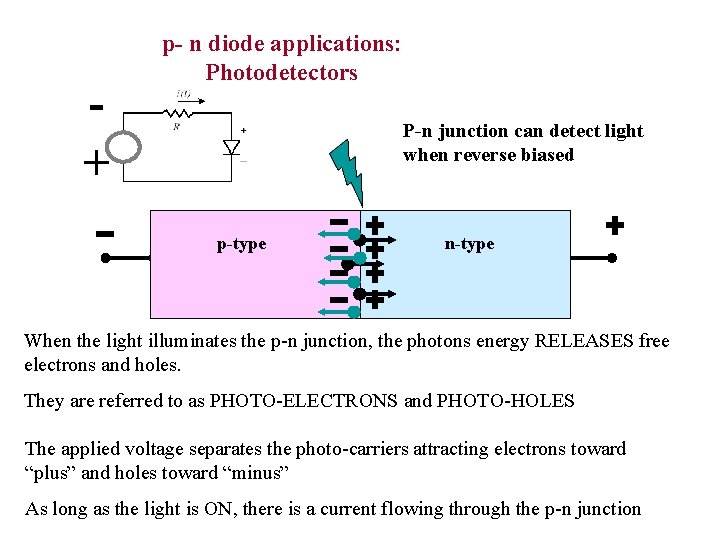
p- n diode applications: Photodetectors + - P-n junction can detect light when reverse biased p-type n-type When the light illuminates the p-n junction, the photons energy RELEASES free electrons and holes. They are referred to as PHOTO-ELECTRONS and PHOTO-HOLES The applied voltage separates the photo-carriers attracting electrons toward “plus” and holes toward “minus” As long as the light is ON, there is a current flowing through the p-n junction

NEGATIVE RESISTANCE DEVICE • It is a device which exhibits a negative incremental resistance over a limited range of VI characteristic. • It is of two types : 1. Current controllable type : V-I curve is a multi valued function of voltage and single valued function of current. eg: - UJT, p-n-p-n diode 2. Voltage controllable type : V-I curve is a multi valued function of current and single valued function of voltage. eg: - SCS, Tunnel diode

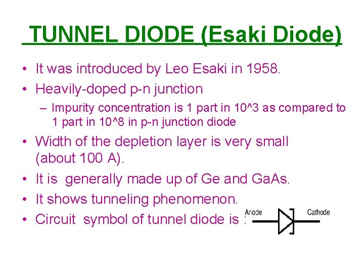
TUNNEL DIODE (Esaki Diode) • It was introduced by Leo Esaki in 1958. • Heavily-doped p-n junction EV – Impurity concentration is 1 part in 10^3 as compared to 1 part in 10^8 in p-n junction diode • Width of the depletion layer is very small (about 100 A). • It is generally made up of Ge and Ga. As. • It shows tunneling phenomenon. • Circuit symbol of tunnel diode is :

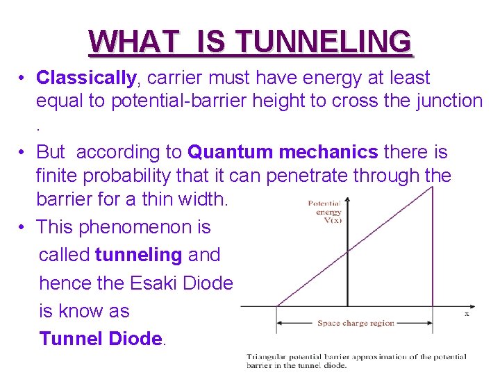
WHAT IS TUNNELING • Classically, carrier must have energy at least equal to potential-barrier height to cross the junction. • But according to Quantum mechanics there is finite probability that it can penetrate through the barrier for a thin width. • This phenomenon is called tunneling and hence the Esaki Diode is know as Tunnel Diode.

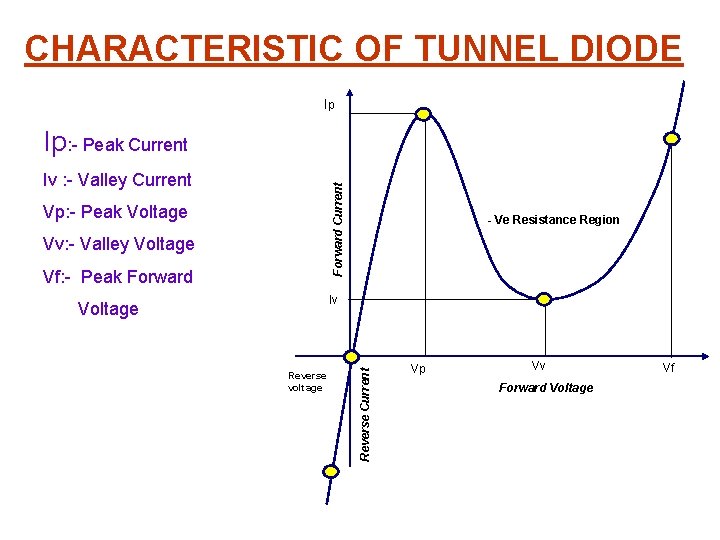
CHARACTERISTIC OF TUNNEL DIODE Ip Ip: - Peak Current Forward Current Iv : - Valley Current Vp: - Peak Voltage Vv: - Valley Voltage Vf: - Peak Forward - Ve Resistance Region Reverse voltage Reverse Current Iv Voltage Vp Vv Forward Voltage Vf

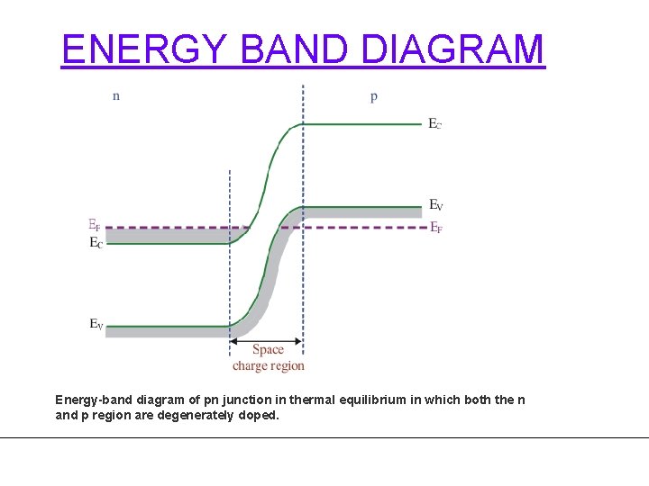
ENERGY BAND DIAGRAM Energy-band diagram of pn junction in thermal equilibrium in which both the n and p region are degenerately doped.

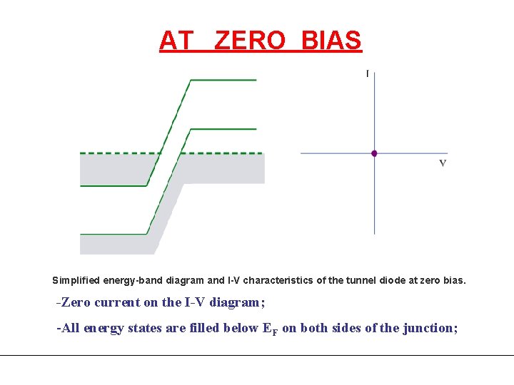
AT ZERO BIAS Simplified energy-band diagram and I-V characteristics of the tunnel diode at zero bias. -Zero current on the I-V diagram; -All energy states are filled below EF on both sides of the junction;

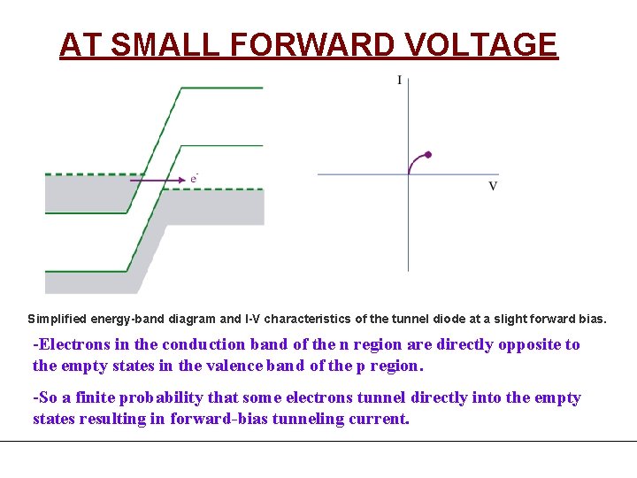
AT SMALL FORWARD VOLTAGE Simplified energy-band diagram and I-V characteristics of the tunnel diode at a slight forward bias. -Electrons in the conduction band of the n region are directly opposite to the empty states in the valence band of the p region. -So a finite probability that some electrons tunnel directly into the empty states resulting in forward-bias tunneling current.

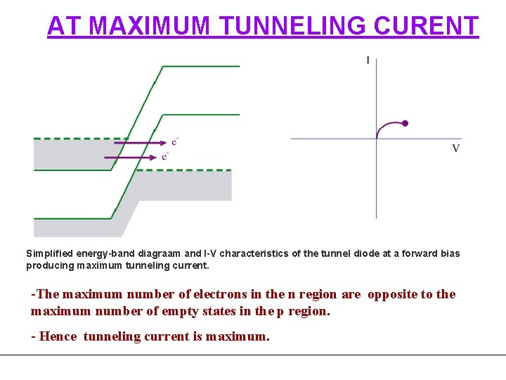
AT MAXIMUM TUNNELING CURENT Simplified energy-band diagraam and I-V characteristics of the tunnel diode at a forward bias producing maximum tunneling current. -The maximum number of electrons in the n region are opposite to the maximum number of empty states in the p region. - Hence tunneling current is maximum.

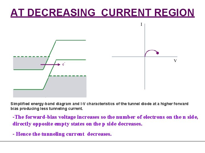
AT DECREASING CURRENT REGION Simplified energy-band diagram and I-V characteristics of the tunnel diode at a higher forward bias producing less tunneling current. -The forward-bias voltage increases so the number of electrons on the n side, directly opposite empty states on the p side decreases. - Hence the tunneling current decreases.

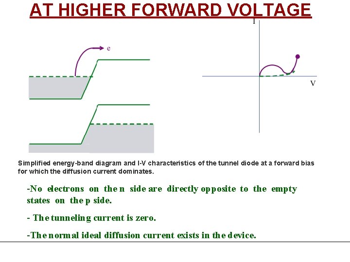
AT HIGHER FORWARD VOLTAGE Simplified energy-band diagram and I-V characteristics of the tunnel diode at a forward bias for which the diffusion current dominates. -No electrons on the n side are directly opposite to the empty states on the p side. - The tunneling current is zero. -The normal ideal diffusion current exists in the device.

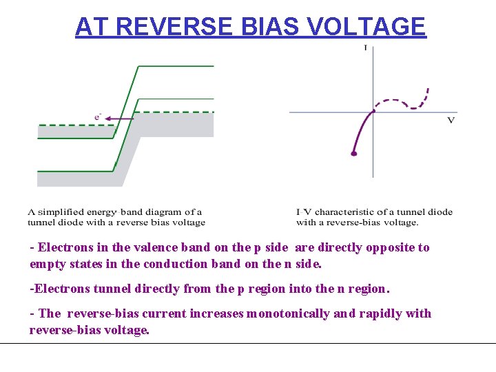
AT REVERSE BIAS VOLTAGE - Electrons in the valence band on the p side are directly opposite to empty states in the conduction band on the n side. -Electrons tunnel directly from the p region into the n region. - The reverse-bias current increases monotonically and rapidly with reverse-bias voltage.

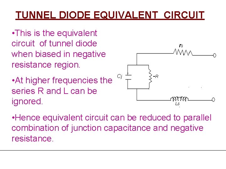
TUNNEL DIODE EQUIVALENT CIRCUIT • This is the equivalent circuit of tunnel diode when biased in negative resistance region. • At higher frequencies the series R and L can be ignored. rs Cj -R Ls • Hence equivalent circuit can be reduced to parallel combination of junction capacitance and negative resistance.

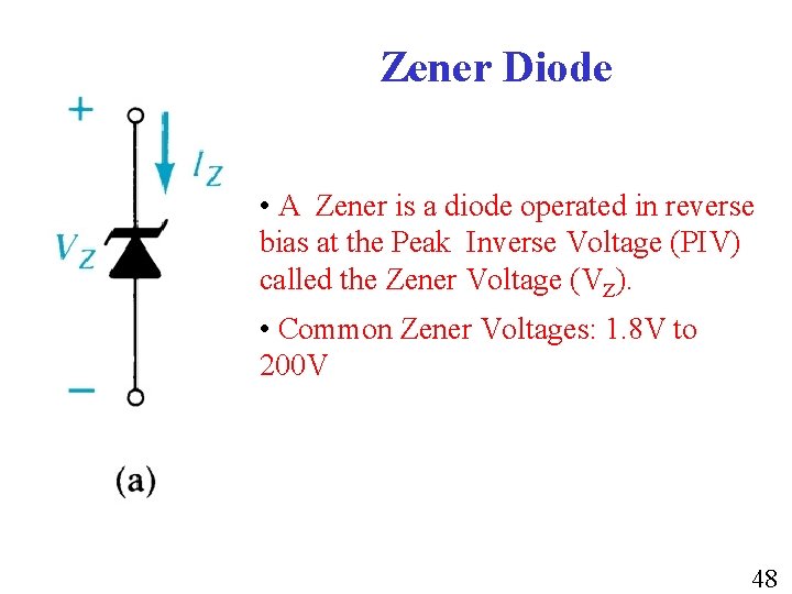
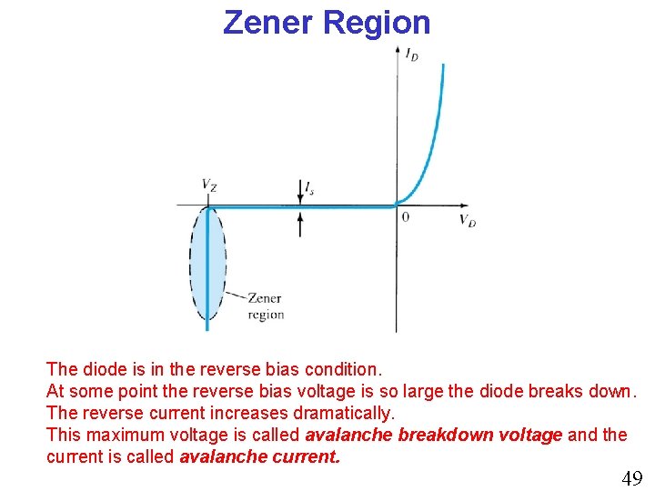
Zener Diode • A Zener is a diode operated in reverse bias at the Peak Inverse Voltage (PIV) called the Zener Voltage (VZ). • Common Zener Voltages: 1. 8 V to 200 V 48

Zener Region The diode is in the reverse bias condition. At some point the reverse bias voltage is so large the diode breaks down. The reverse current increases dramatically. This maximum voltage is called avalanche breakdown voltage and the current is called avalanche current. 49

Resistance Levels Semiconductors act differently to DC and AC currents. There are 3 types of resistances. • DC or Static Resistance • AC or Dynamic Resistance • Average AC Resistance 50

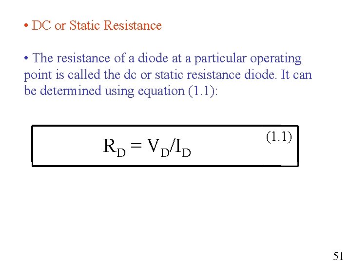
• DC or Static Resistance • The resistance of a diode at a particular operating point is called the dc or static resistance diode. It can be determined using equation (1. 1): RD = VD/ID (1. 1) 51

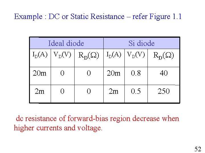
Example : DC or Static Resistance – refer Figure 1. 1 Ideal diode Si diode ID(A) VD(V) RD( ) 20 m 0 0 20 m 0. 8 40 2 m 0. 5 250 dc resistance of forward-bias region decrease when higher currents and voltage. 52

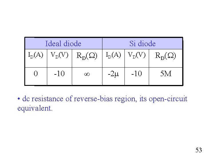
Ideal diode ID(A) VD(V) RD( ) 0 -10 Si diode ID(A) VD(V) RD( ) -2 -10 5 M • dc resistance of reverse-bias region, its open-circuit equivalent. 53

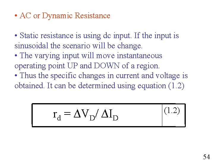
• AC or Dynamic Resistance • Static resistance is using dc input. If the input is sinusoidal the scenario will be change. • The varying input will move instantaneous operating point UP and DOWN of a region. • Thus the specific changes in current and voltage is obtained. It can be determined using equation (1. 2) rd = ∆VD/ ∆ID (1. 2) 54

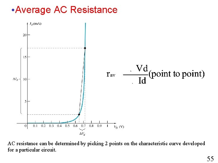
• Average AC Resistance AC resistance can be determined by picking 2 points on the characteristic curve developed for a particular circuit. 55