PN Junction Diodes Current Flowing through a Diode

![(d) Adapted from [8]. Current-voltage characteristic for a diode near the boundary between (a) (d) Adapted from [8]. Current-voltage characteristic for a diode near the boundary between (a)](https://slidetodoc.com/presentation_image/f5e9da32b90a5f7089f127b368bd77dd/image-27.jpg)
- Slides: 35

P-N Junction Diodes Current Flowing through a Diode I-V Characteristics Quantitative Analysis (Math, math and more math)

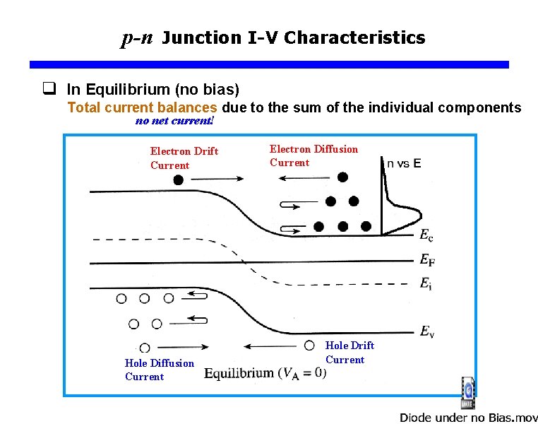
p-n Junction I-V Characteristics q In Equilibrium (no bias) Total current balances due to the sum of the individual components no net current! Electron Drift Current Hole Diffusion Current Electron Diffusion Current Hole Drift Current

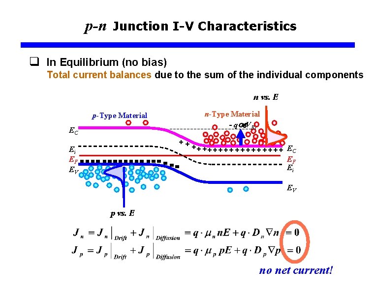
p-n Junction I-V Characteristics q In Equilibrium (no bias) Total current balances due to the sum of the individual components n vs. E n-Type Material - q VBI p-Type Material EC ++ Ei EF EV + + + + + EC EF Ei EV p vs. E no net current!

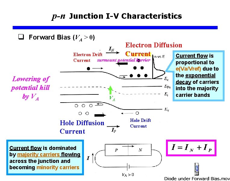
p-n Junction I-V Characteristics q Forward Bias (VA > 0) IN Electron Diffusion Current flow is Electron Drift Current surmount potential barrier Lowering of potential hill by VA VA Hole Diffusion Current flow is dominated by majority carriers flowing across the junction and becoming minority carriers I IP Hole Drift Current proportional to e(Va/Vref) due to the exponential decay of carriers into the majority carrier bands

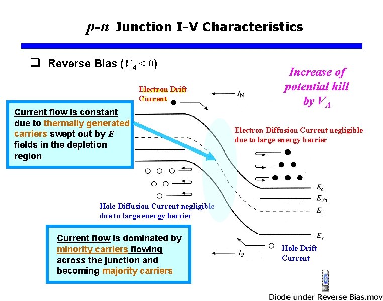
p-n Junction I-V Characteristics q Reverse Bias (VA < 0) Electron Drift Current flow is constant due to thermally generated carriers swept out by E fields in the depletion region Increase of potential hill by VA Electron Diffusion Current negligible due to large energy barrier Hole Diffusion Current negligible due to large energy barrier Current flow is dominated by minority carriers flowing across the junction and becoming majority carriers Hole Drift Current

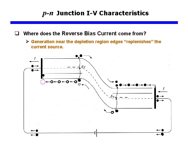
p-n Junction I-V Characteristics q Where does the Reverse Bias Current come from? Ø Generation near the depletion region edges “replenishes” the current source.

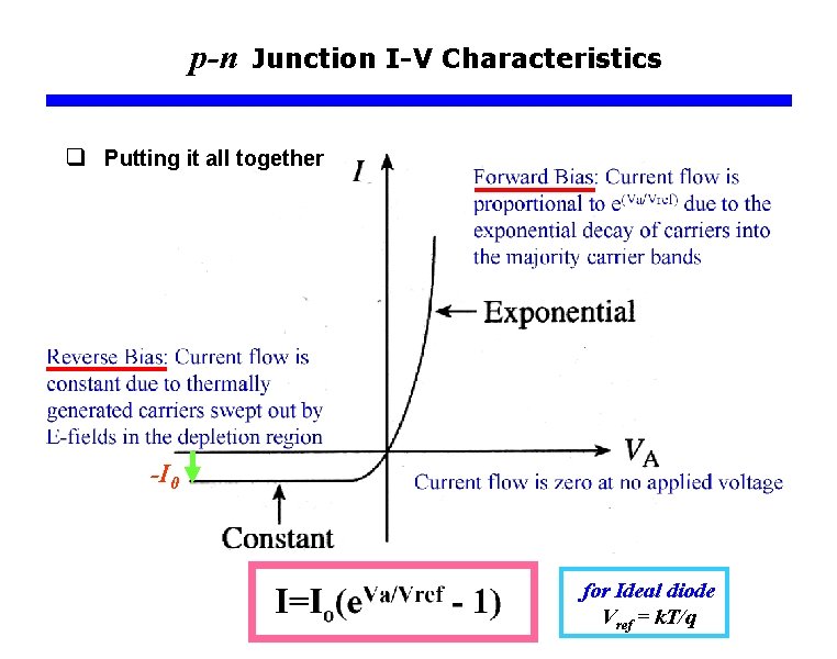
p-n Junction I-V Characteristics q Putting it all together -I 0 for Ideal diode Vref = k. T/q

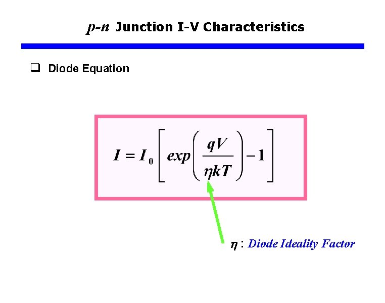
p-n Junction I-V Characteristics q Diode Equation : Diode Ideality Factor

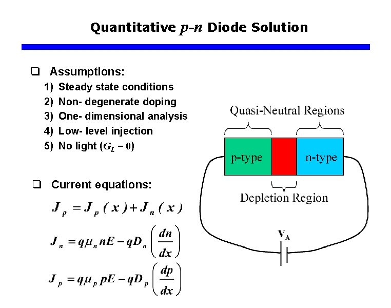
Quantitative p-n Diode Solution q Assumptions: 1) 2) 3) 4) 5) Steady state conditions Non- degenerate doping One- dimensional analysis Low- level injection No light (GL = 0) q Current equations:

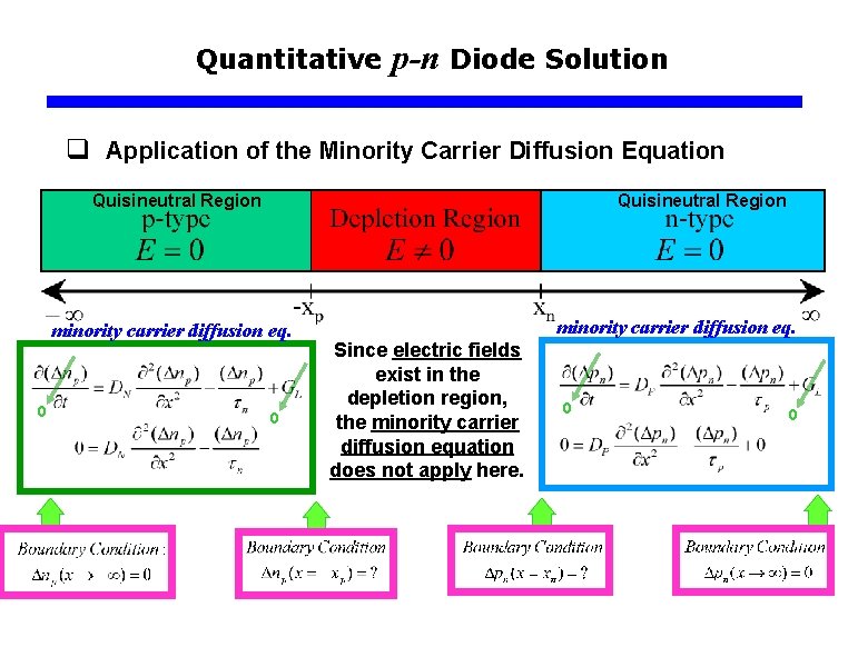
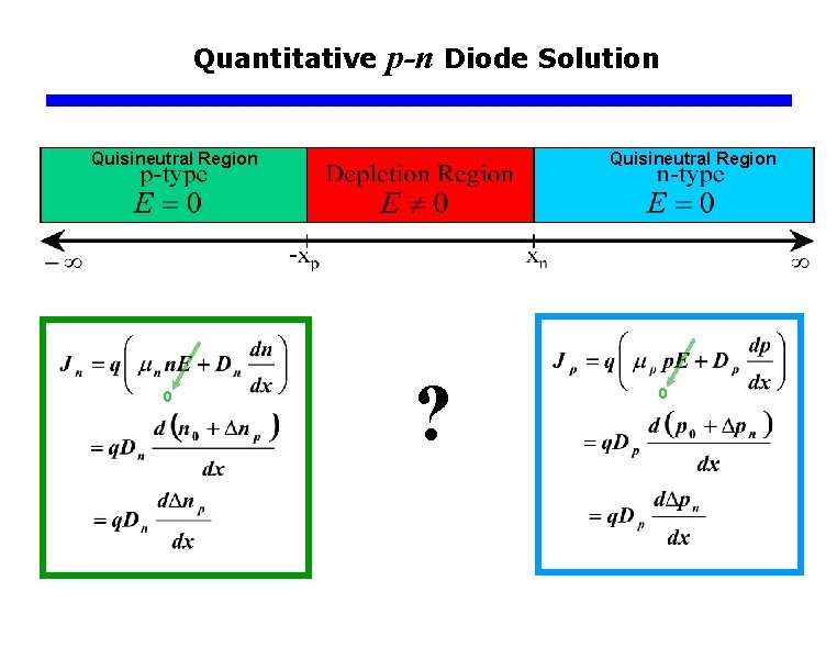
Quantitative p-n Diode Solution q Application of the Minority Carrier Diffusion Equation Quisineutral Region minority carrier diffusion eq. 0 0 minority carrier diffusion eq. Since electric fields exist in the depletion region, the minority carrier diffusion equation does not apply here. 0 0

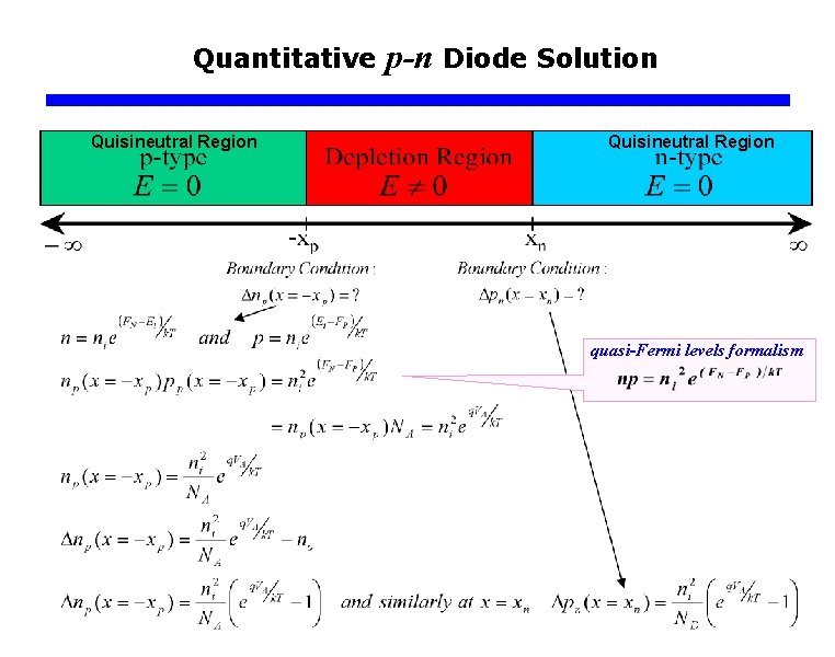
Quantitative Quisineutral Region p-n Diode Solution Quisineutral Region quasi-Fermi levels formalism

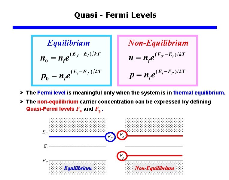
Quasi - Fermi Levels Equilibrium Non-Equilibrium Ø The Fermi level is meaningful only when the system is in thermal equilibrium. Ø The non-equilibrium carrier concentration can be expressed by defining Quasi-Fermi levels Fn and Fp. Equilibrium Non-Equilibrium

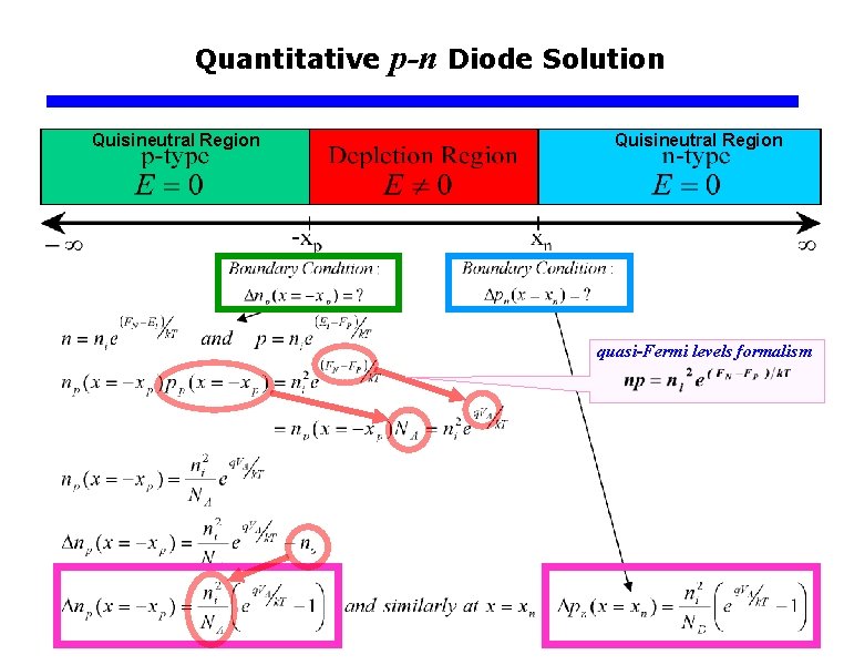
Quantitative Quisineutral Region p-n Diode Solution Quisineutral Region quasi-Fermi levels formalism

Quantitative p-n Diode Solution Quisineutral Region 0 Quisineutral Region ? 0

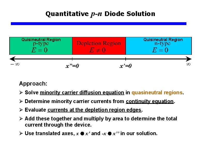
Quantitative p-n Diode Solution Quisineutral Region x”=0 x’=0 Approach: Ø Solve minority carrier diffusion equation in quasineutral regions. Ø Determine minority carrier currents from continuity equation. Ø Evaluate currents at the depletion region edges. Ø Add these together and multiply by area to determine the total current through the device. Ø Use translated axes, x x’ and -x x’’ in our solution.

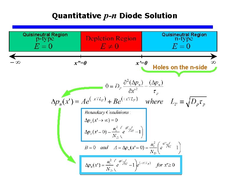
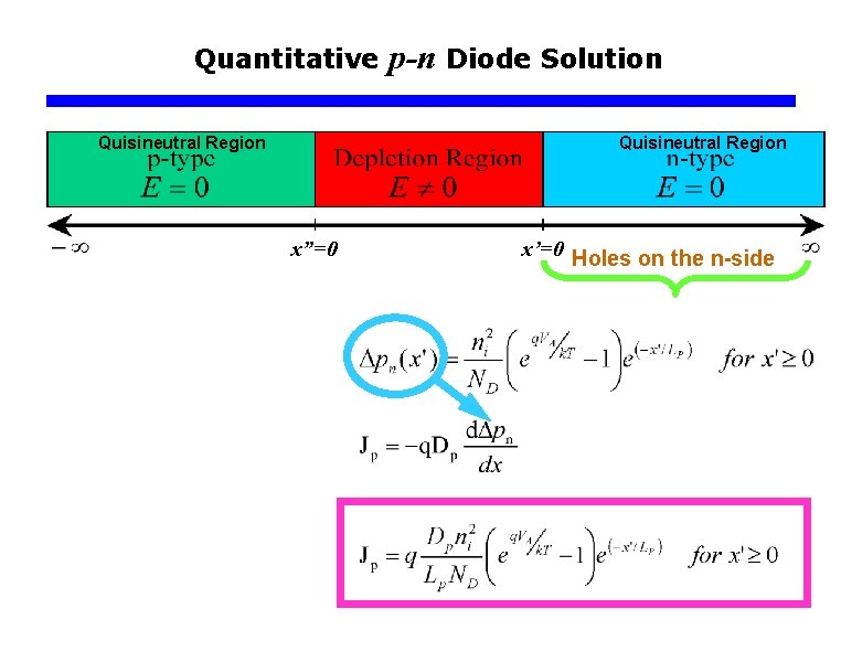
Quantitative p-n Diode Solution Quisineutral Region x”=0 x’=0 Holes on the n-side

Quantitative Quisineutral Region p-n Diode Solution Quisineutral Region x”=0 x’=0 Holes on the n-side

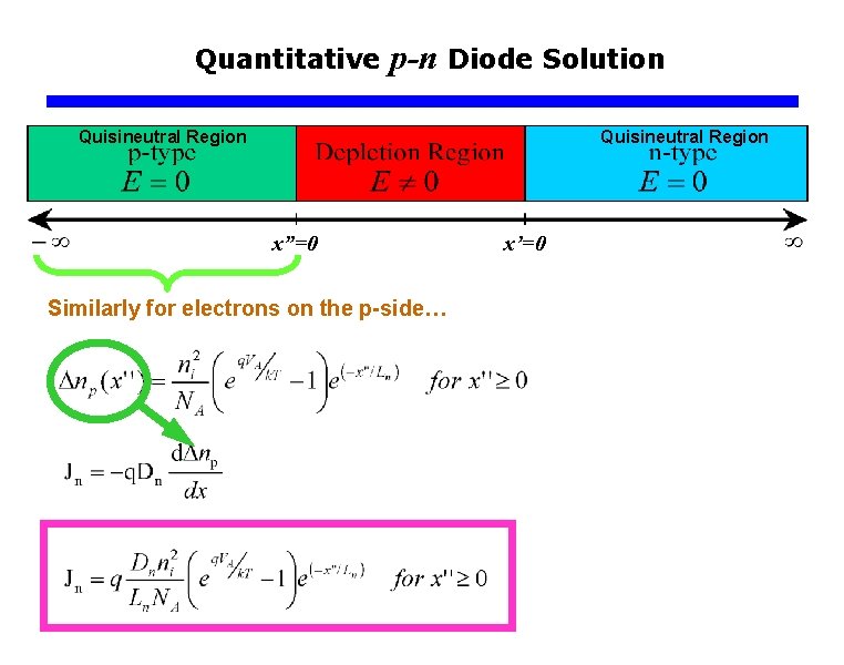
Quantitative p-n Diode Solution Quisineutral Region x”=0 Similarly for electrons on the p-side… x’=0

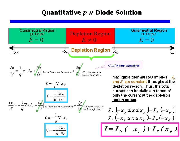
Quantitative p-n Diode Solution Quisineutral Region Depletion Region Continuity equation 0 0 0 Negligible thermal R-G implies Jn and Jp are constant throughout the depletion region. Thus, the total current can be define in terms of only the current at the depletion region edges. 0

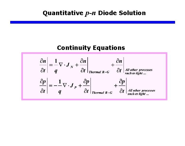
Quantitative p-n Diode Solution Continuity Equations

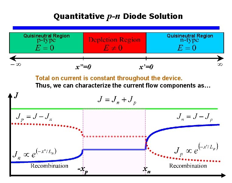
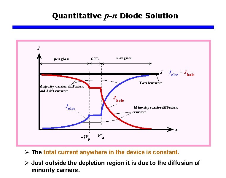
Quantitative p-n Diode Solution Quisineutral Region x”=0 x’=0 Total on current is constant throughout the device. Thus, we can characterize the current flow components as… J -xp xn

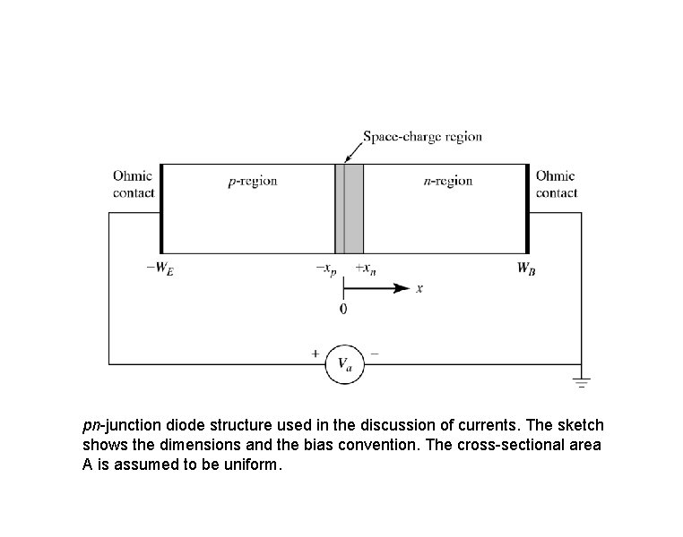
pn-junction diode structure used in the discussion of currents. The sketch shows the dimensions and the bias convention. The cross-sectional area A is assumed to be uniform.

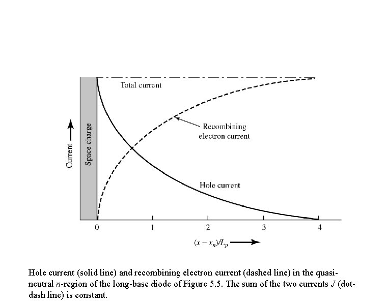
Hole current (solid line) and recombining electron current (dashed line) in the quasineutral n-region of the long-base diode of Figure 5. 5. The sum of the two currents J (dotdash line) is constant.

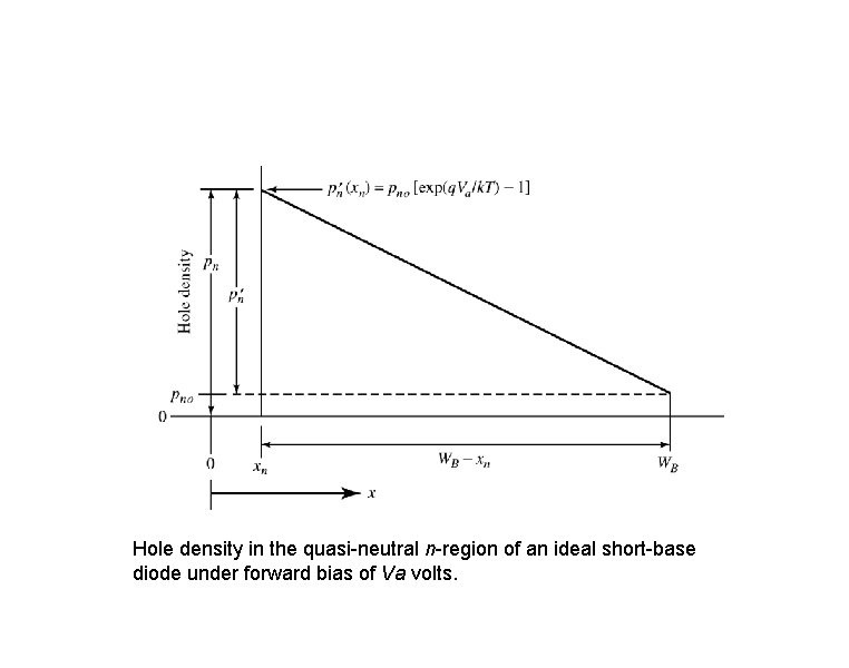
Hole density in the quasi-neutral n-region of an ideal short-base diode under forward bias of Va volts.

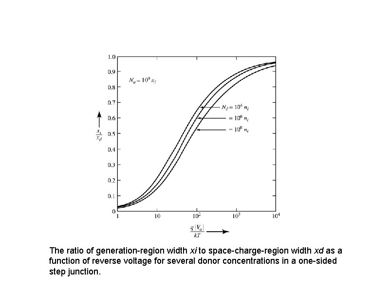
The ratio of generation-region width xi to space-charge-region width xd as a function of reverse voltage for several donor concentrations in a one-sided step junction.

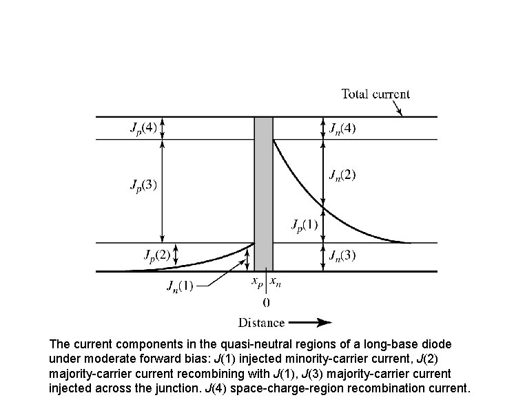
The current components in the quasi-neutral regions of a long-base diode under moderate forward bias: J(1) injected minority-carrier current, J(2) majority-carrier current recombining with J(1), J(3) majority-carrier current injected across the junction. J(4) space-charge-region recombination current.
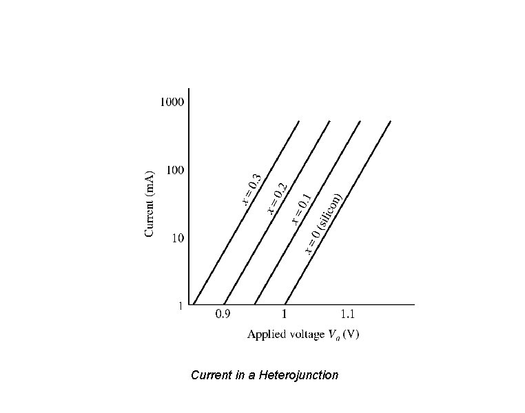
![d Adapted from 8 Currentvoltage characteristic for a diode near the boundary between a (d) Adapted from [8]. Current-voltage characteristic for a diode near the boundary between (a)](https://slidetodoc.com/presentation_image/f5e9da32b90a5f7089f127b368bd77dd/image-27.jpg)
(d) Adapted from [8]. Current-voltage characteristic for a diode near the boundary between (a) and (c), showing diffusion current at lower voltages and a transition to thermionic-emission current at higher biases.

Current in a Heterojunction

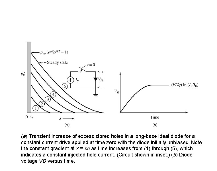
(a) Transient increase of excess stored holes in a long-base ideal diode for a constant current drive applied at time zero with the diode initially unbiased. Note the constant gradient at x = xn as time increases from (1) through (5), which indicates a constant injected hole current. (Circuit shown in inset. ) (b) Diode voltage VD versus time.

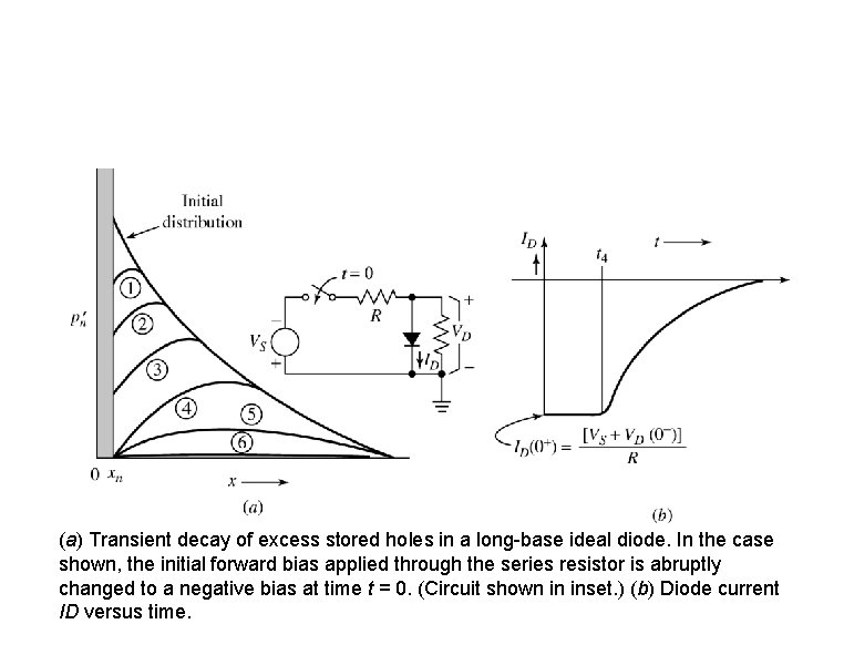
(a) Transient decay of excess stored holes in a long-base ideal diode. In the case shown, the initial forward bias applied through the series resistor is abruptly changed to a negative bias at time t = 0. (Circuit shown in inset. ) (b) Diode current ID versus time.

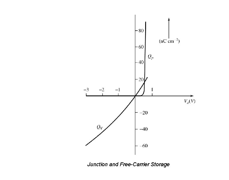
Junction and Free-Carrier Storage

Quantitative p-n Diode Solution J p-region SCL n-region J = J elec + J hole Total current Majority carrier diffusion and drift current J h ole J elec Minority carrier diffusion current x –W p Wn Ø The total current anywhere in the device is constant. Ø Just outside the depletion region it is due to the diffusion of minority carriers.

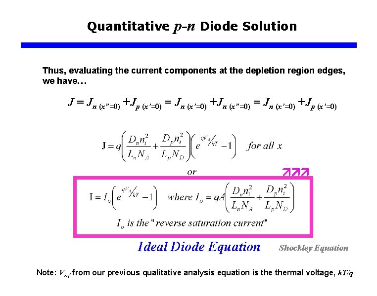
Quantitative p-n Diode Solution Thus, evaluating the current components at the depletion region edges, we have… J = Jn (x”=0) +Jp (x’=0) = Jn (x’=0) +Jn (x”=0) = Jn (x’=0) +Jp (x’=0) Ideal Diode Equation Shockley Equation Note: Vref from our previous qualitative analysis equation is thermal voltage, k. T/q

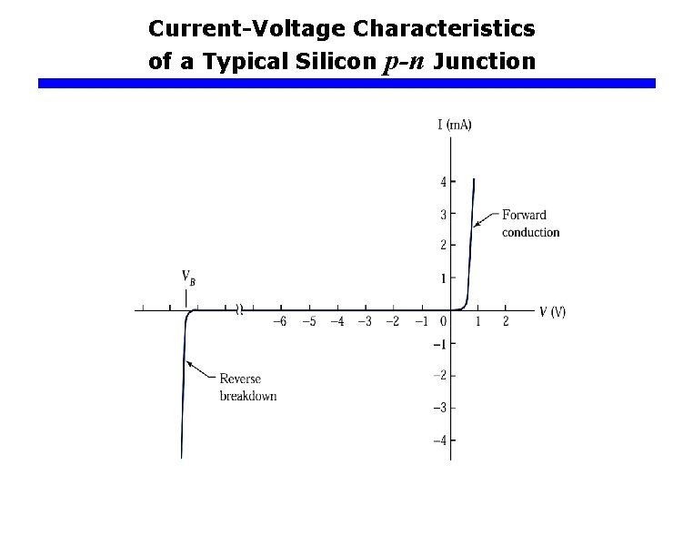
Current-Voltage Characteristics of a Typical Silicon p-n Junction

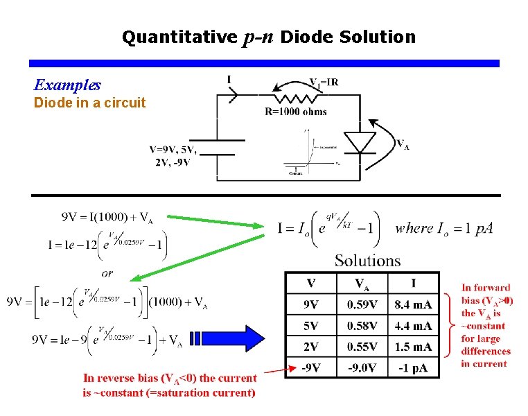
Quantitative Examples Diode in a circuit p-n Diode Solution