Nishina School Lecture 2009 Semiconductor Detectors Shunji Nishimura
![Detectors General Requirements [ Particle Identification ] We want to detect the particle positively. Detectors General Requirements [ Particle Identification ] We want to detect the particle positively.](https://slidetodoc.com/presentation_image_h/9bd0f13b86756f1c553187ce720fdca9/image-3.jpg)

![Basic Principles [ To dope the silicon with impurities ] Boron doping ( p-type Basic Principles [ To dope the silicon with impurities ] Boron doping ( p-type](https://slidetodoc.com/presentation_image_h/9bd0f13b86756f1c553187ce720fdca9/image-8.jpg)
![Basic Principles [Semiconductor structure] - + + ++ -+ ++- + + - - Basic Principles [Semiconductor structure] - + + ++ -+ ++- + + - -](https://slidetodoc.com/presentation_image_h/9bd0f13b86756f1c553187ce720fdca9/image-11.jpg)
![Energy Resolution [ Signal to Background Ratio (S/N) ] Good Energy Resolution Higher Statistics Energy Resolution [ Signal to Background Ratio (S/N) ] Good Energy Resolution Higher Statistics](https://slidetodoc.com/presentation_image_h/9bd0f13b86756f1c553187ce720fdca9/image-19.jpg)
![Particle Identification [ Use Difference of Stopping Power ] For very low momenta, we Particle Identification [ Use Difference of Stopping Power ] For very low momenta, we](https://slidetodoc.com/presentation_image_h/9bd0f13b86756f1c553187ce720fdca9/image-20.jpg)
![Particle Identification [ d. E-E Correlation] Motobayashi-san’s lecture Multi-layer detectors enable us to identify Particle Identification [ d. E-E Correlation] Motobayashi-san’s lecture Multi-layer detectors enable us to identify](https://slidetodoc.com/presentation_image_h/9bd0f13b86756f1c553187ce720fdca9/image-21.jpg)
![Energy Resolution : [ Temperature Dependence ] Semiconductor Detectors prefer COOLING ! Energy Resolution : [ Temperature Dependence ] Semiconductor Detectors prefer COOLING !](https://slidetodoc.com/presentation_image_h/9bd0f13b86756f1c553187ce720fdca9/image-22.jpg)
![Electronics [ Signal Integration on Input Capacitance ] H. Spieler’s Lecture (LBNL) Energy Deposit Electronics [ Signal Integration on Input Capacitance ] H. Spieler’s Lecture (LBNL) Energy Deposit](https://slidetodoc.com/presentation_image_h/9bd0f13b86756f1c553187ce720fdca9/image-31.jpg)


- Slides: 41

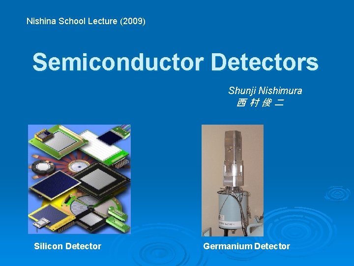
Nishina School Lecture (2009) Semiconductor Detectors Shunji Nishimura 西村俊二 Silicon Detector Germanium Detector

Outline of this Lecture Ø Introduction l l Ø Basic Principles l l l Ø Detectors General Requirements Why use semiconductor detectors? P-type, N-type Depletion layer Type of detectors Performance l l l Energy Measurement Position Measurement Timing Measurement Ø Electronics Ø Operation : How to use?
![Detectors General Requirements Particle Identification We want to detect the particle positively Detectors General Requirements [ Particle Identification ] We want to detect the particle positively.](https://slidetodoc.com/presentation_image_h/9bd0f13b86756f1c553187ce720fdca9/image-3.jpg)
Detectors General Requirements [ Particle Identification ] We want to detect the particle positively. - what kind of particles? ! - momentum, direction, time, etc. . Hadrons proton, neutron, d, t, 3 He, … pion, kaon, … Photon Gamma-ray (g) Lepton Electron (b), Muon (m), Tau(t) Neutrino (n)

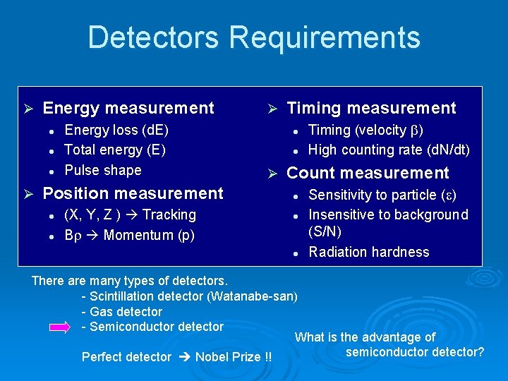
Detectors Requirements Ø Energy measurement l l l Ø Energy loss (d. E) Total energy (E) Pulse shape Position measurement l l (X, Y, Z ) Tracking Br Momentum (p) Ø Timing measurement l l Ø Timing (velocity b) High counting rate (d. N/dt) Count measurement l l l Sensitivity to particle (e) Insensitive to background (S/N) Radiation hardness There are many types of detectors. - Scintillation detector (Watanabe-san) - Gas detector - Semiconductor detector What is the advantage of semiconductor detector? Perfect detector Nobel Prize !!

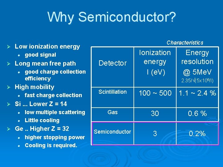
Why Semiconductor? Ø Low ionization energy l Ø fast charge collection Ionization energy I (e. V) Energy resolution @ 5 Me. V 2. 35/√(5 x 106/I) Scintillation 100 ~ 500 1. 1 ~ 2. 4 % Si. . . Lower Z = 14 l l Ø Detector good charge collection efficiency High mobility l Ø good signal Long mean free path l Ø Characteristics low multiple scattering Little cooling Ge. . Higher Z = 32 l l higher stopping power Cooling is required. Gas 30 0. 6 % Semiconductor 3 0. 2%

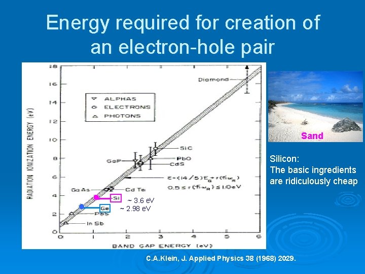
Energy required for creation of an electron-hole pair Sand Silicon: The basic ingredients are ridiculously cheap ~ 3. 6 e. V ~ 2. 98 e. V C. A. Klein, J. Applied Physics 38 (1968) 2029.

Basic Principles
![Basic Principles To dope the silicon with impurities Boron doping ptype Basic Principles [ To dope the silicon with impurities ] Boron doping ( p-type](https://slidetodoc.com/presentation_image_h/9bd0f13b86756f1c553187ce720fdca9/image-8.jpg)
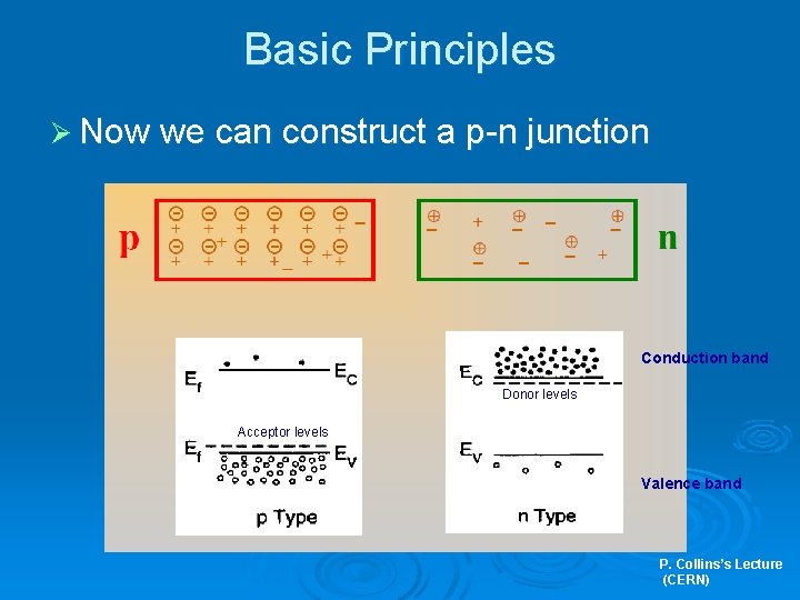
Basic Principles [ To dope the silicon with impurities ] Boron doping ( p-type ) holes are majority carriers Phosphorus doping ( n-type ) electrons are majority carriers From : Radiation Detection and Mesurement by Knoll

Basic Principles Ø Now we can construct a p-n junction Conduction band Donor levels Acceptor levels Valence band P. Collins’s Lecture (CERN)

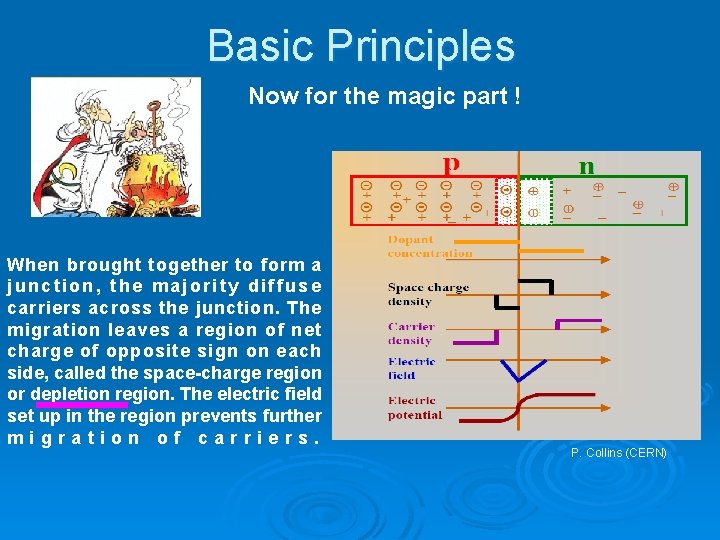
Basic Principles Now for the magic part ! When brought together to form a junction, the majority diffuse carriers across the junction. The migration leaves a region of net charge of opposite sign on each side, called the space-charge region or depletion region. The electric field set up in the region prevents further migration of carriers. P. Collins (CERN)
![Basic Principles Semiconductor structure Basic Principles [Semiconductor structure] - + + ++ -+ ++- + + - -](https://slidetodoc.com/presentation_image_h/9bd0f13b86756f1c553187ce720fdca9/image-11.jpg)
Basic Principles [Semiconductor structure] - + + ++ -+ ++- + + - - p n p Use ionization signal left behind by charged particle passage. Ø Ionization produces electron(e)-ion(h) pairs, use electric field to drift the e and h to the oppositely charged electrodes. Ø Si needs 3. 6 e. V to produce one e-h pair. n E P Region Ø N Region

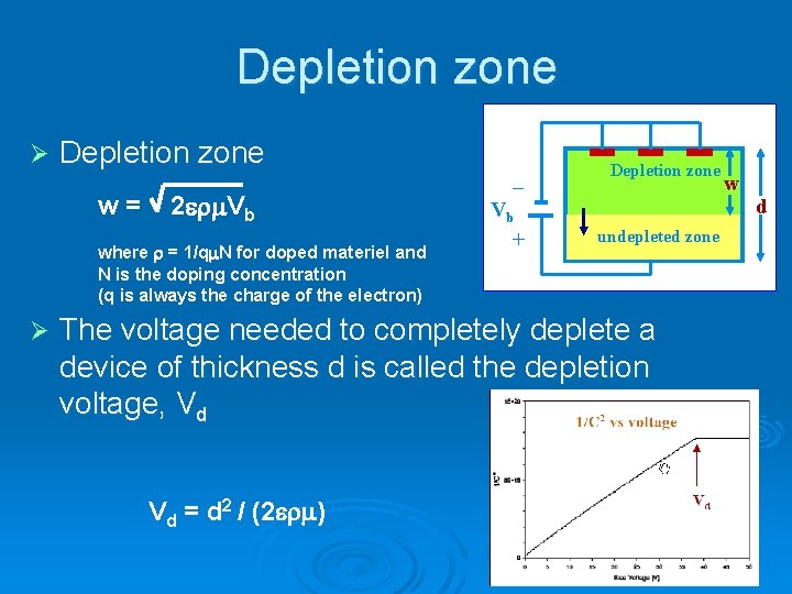
Depletion zone Ø Depletion zone w= 2 Vb where = 1/q N for doped materiel and N is the doping concentration (q is always the charge of the electron) Ø – Vb + Depletion zone undepleted zone The voltage needed to completely deplete a device of thickness d is called the depletion voltage, Vd Vd = d 2 / (2 ) w d

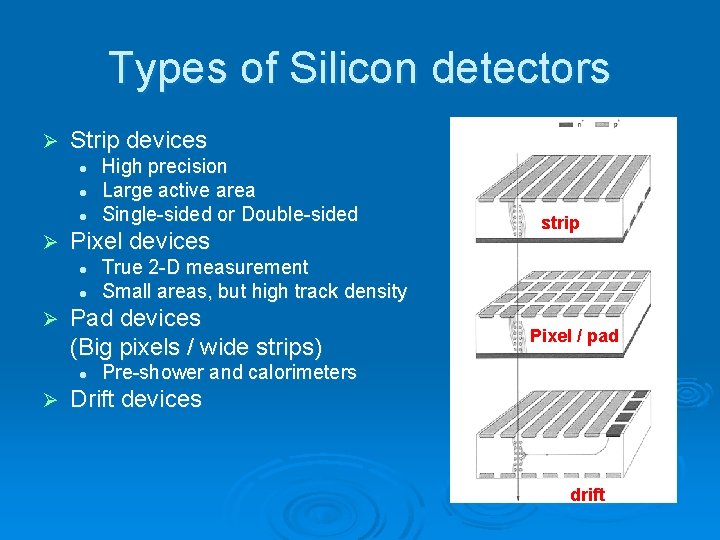
Types of Silicon detectors Ø Strip devices l l l Ø Pixel devices l l Ø strip True 2 -D measurement Small areas, but high track density Pad devices (Big pixels / wide strips) l Ø High precision Large active area Single-sided or Double-sided Pixel / pad Pre-shower and calorimeters Drift devices drift

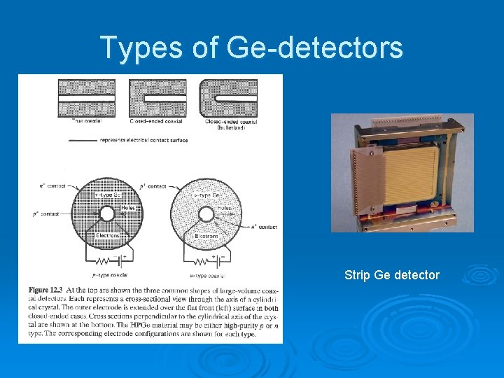
Types of Ge-detectors Strip Ge detector

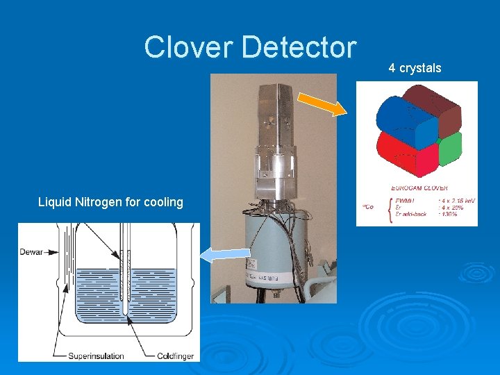
Clover Detector Liquid Nitrogen for cooling 4 crystals

Performance I Energy Resolution

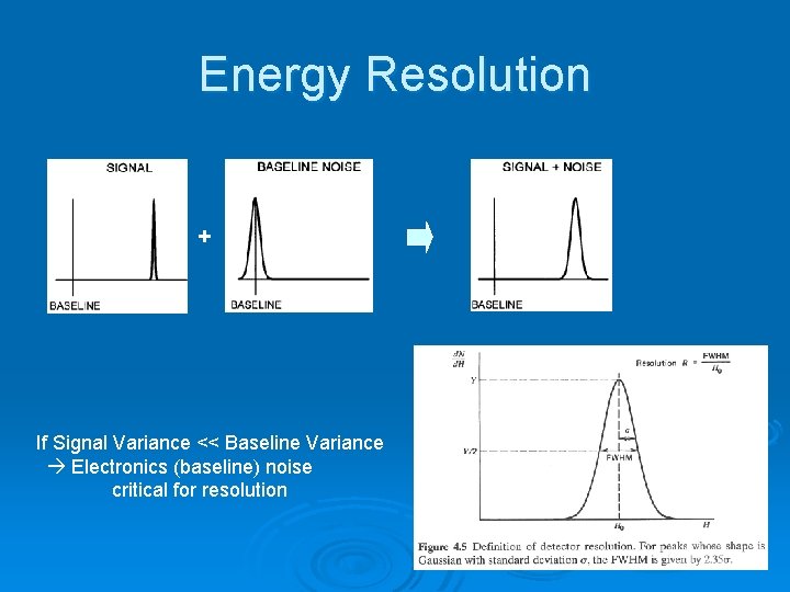
Energy Resolution + If Signal Variance << Baseline Variance Electronics (baseline) noise critical for resolution

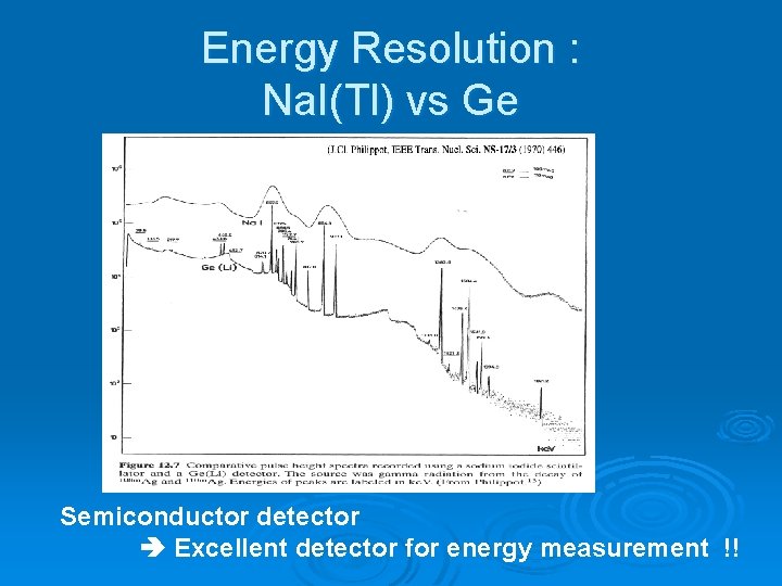
Energy Resolution : Na. I(Tl) vs Ge Semiconductor detector Excellent detector for energy measurement !!
![Energy Resolution Signal to Background Ratio SN Good Energy Resolution Higher Statistics Energy Resolution [ Signal to Background Ratio (S/N) ] Good Energy Resolution Higher Statistics](https://slidetodoc.com/presentation_image_h/9bd0f13b86756f1c553187ce720fdca9/image-19.jpg)
Energy Resolution [ Signal to Background Ratio (S/N) ] Good Energy Resolution Higher Statistics We can extract - precise peak position, - and find NEW Peaks!!
![Particle Identification Use Difference of Stopping Power For very low momenta we Particle Identification [ Use Difference of Stopping Power ] For very low momenta, we](https://slidetodoc.com/presentation_image_h/9bd0f13b86756f1c553187ce720fdca9/image-20.jpg)
Particle Identification [ Use Difference of Stopping Power ] For very low momenta, we can exploit the bethe-bloch formula for particle identification Knowing p and b gives m Lecture by Taketani-san
![Particle Identification d EE Correlation Motobayashisans lecture Multilayer detectors enable us to identify Particle Identification [ d. E-E Correlation] Motobayashi-san’s lecture Multi-layer detectors enable us to identify](https://slidetodoc.com/presentation_image_h/9bd0f13b86756f1c553187ce720fdca9/image-21.jpg)
Particle Identification [ d. E-E Correlation] Motobayashi-san’s lecture Multi-layer detectors enable us to identify the particles!
![Energy Resolution Temperature Dependence Semiconductor Detectors prefer COOLING Energy Resolution : [ Temperature Dependence ] Semiconductor Detectors prefer COOLING !](https://slidetodoc.com/presentation_image_h/9bd0f13b86756f1c553187ce720fdca9/image-22.jpg)
Energy Resolution : [ Temperature Dependence ] Semiconductor Detectors prefer COOLING !

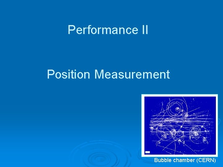
Performance II Position Measurement Bubble chamber (CERN)

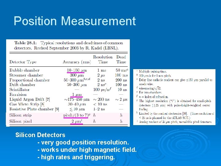
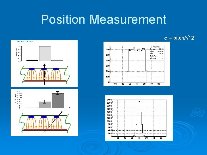
Position Measurement Silicon Detectors - very good position resolution. - works under high magnetic field. - high rates and triggering.

Position Measurement s = pitch/√ 12

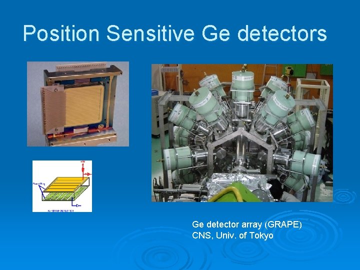
Position Sensitive Ge detectors Ge detector array (GRAPE) CNS, Univ. of Tokyo

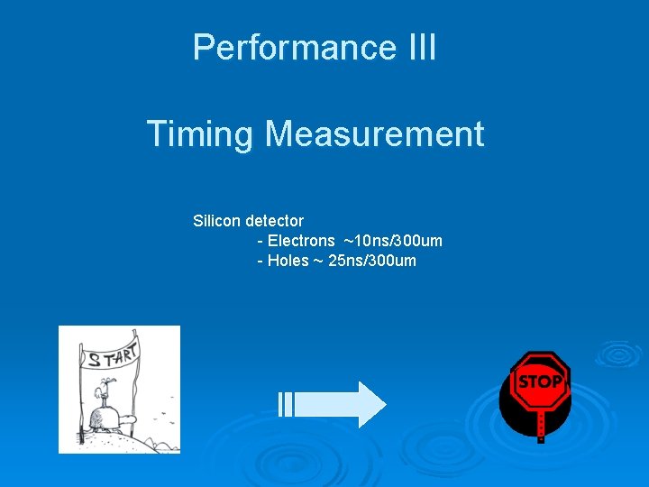
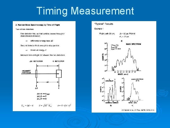
Performance III Timing Measurement Silicon detector - Electrons ~10 ns/300 um - Holes ~ 25 ns/300 um

Timing Measurement

Electronics

Electronics Ø Electric noise is an issue for Silicon/Ge detectors. At 22, 000 e- for a 300 um thick silicon sensor, the signal is relatively small. Signal losses can easily occur depending on electronics, stray capacitances, coupling capacitor, frequency etc. Improve energy resolution Ø Allow a low detection threshold Ø
![Electronics Signal Integration on Input Capacitance H Spielers Lecture LBNL Energy Deposit Electronics [ Signal Integration on Input Capacitance ] H. Spieler’s Lecture (LBNL) Energy Deposit](https://slidetodoc.com/presentation_image_h/9bd0f13b86756f1c553187ce720fdca9/image-31.jpg)
Electronics [ Signal Integration on Input Capacitance ] H. Spieler’s Lecture (LBNL) Energy Deposit ∝ Charge Qd However, ☆Detector capacitance CDET may vary within a system or change with bias voltage. ☆Variation of charge collection in time Tc Make system whose gain (d. Vout/d. Qs) is independent of detector capacitance. Charge sensitive preamp !

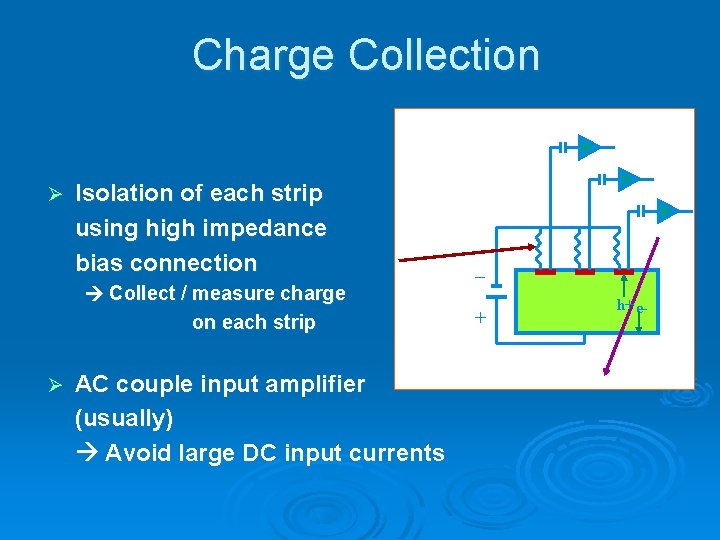
Charge Collection Ø Isolation of each strip using high impedance bias connection Collect / measure charge on each strip Ø AC couple input amplifier (usually) Avoid large DC input currents – + h+ e-

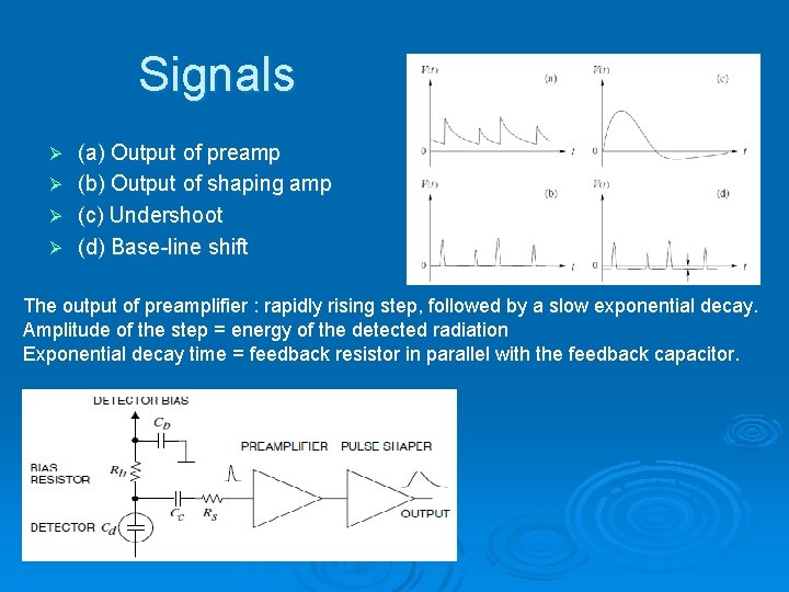
Signals (a) Output of preamp Ø (b) Output of shaping amp Ø (c) Undershoot Ø (d) Base-line shift Ø The output of preamplifier : rapidly rising step, followed by a slow exponential decay. Amplitude of the step = energy of the detected radiation Exponential decay time = feedback resistor in parallel with the feedback capacitor.

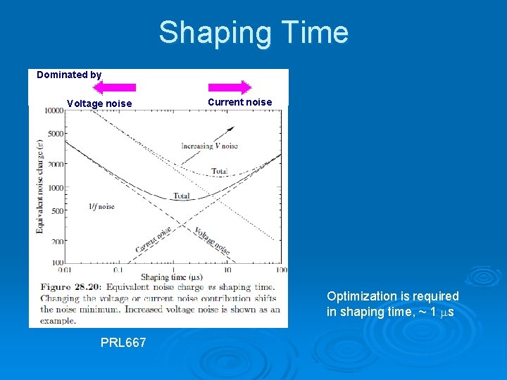
Shaping Time Dominated by Voltage noise Current noise Optimization is required in shaping time, ~ 1 ms PRL 667

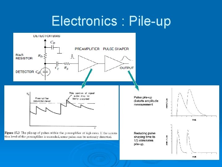
Electronics : Pile-up

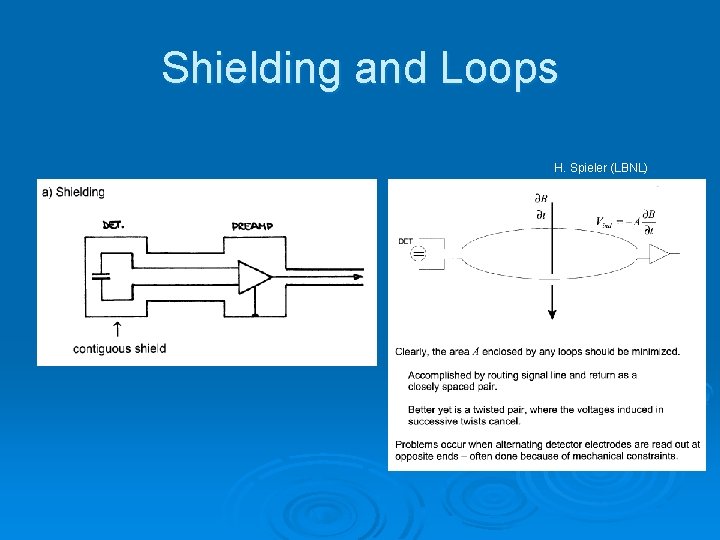
Shielding and Loops H. Spieler (LBNL)

Operation How to use them

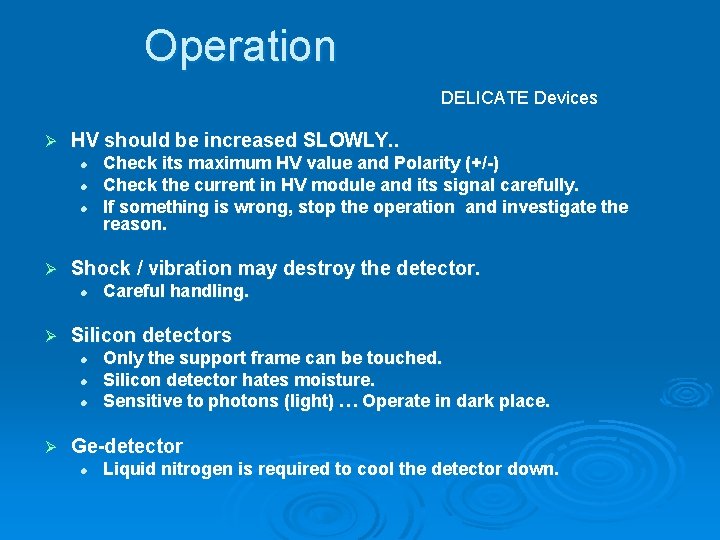
Operation DELICATE Devices Ø HV should be increased SLOWLY. . l l l Ø Shock / vibration may destroy the detector. l Ø Careful handling. Silicon detectors l l l Ø Check its maximum HV value and Polarity (+/-) Check the current in HV module and its signal carefully. If something is wrong, stop the operation and investigate the reason. Only the support frame can be touched. Silicon detector hates moisture. Sensitive to photons (light) … Operate in dark place. Ge-detector l Liquid nitrogen is required to cool the detector down.

Summary Semiconductor detectors based on the simple principle of the p-n junction. Ø Si is typically used for charged particle & X-ray Ø Ge is used for g ray spectroscopy. Ø Friday afternoon, Practical training using Ge detector (by Watanabe-san) I wish you all the best for enjoying your stay in JAPAN !!

References Ø SLAC Lecture l Ø http: //www-group. slac. stanford. edu/sluo/lectures/Detector. Lectures. html Silicon Detector by Paula Collins l http: //lhcb-doc. web. cern. ch/lhcbdoc/presentations/lectures/Collins. Itacuruca 03 -2 nd. pdf REVIEW OF PARTICLE PHYSICS, Phys. Letters B 667 (2008). Ø EG&G ORTEC, Modular Pulse-Processing Electronics and Semiconductor Radiation Detectors. Ø GLENN F. KNOLL, Radiation Detection and Measurement. Ø

End