Semiconductor detectors An introduction to semiconductor detector physics

- Slides: 37

Semiconductor detectors An introduction to semiconductor detector physics as applied to particle physics

Contents 4 lectures – can’t cover much of a huge field • • Introduction Fundamentals of operation The micro-strip detector Radiation hardness issues

Lecture 4 – Radiation Damage • Effects of radiation – Microscopic – Macroscopic – Annealing • What can we do? – – Detector Design Material Engineering Cold Operation Thin detectors/Electrode Structure – 3 -D device

Effects of Radiation • Long Term Ionisation Effects – Trapped charge (holes) in Si. O 2 – interface states at Si. O 2 - Si interface – Can’t use CCD’s in high radiation environment • Displacement Damage in the Si bulk – 4 stage process – Displacement of Silicon atoms from lattice – Formation of long lived point defects & clusters

Displacement Damage • Incoming particle undergoes collision with lattice – knocks out atom = Primary knock on atom • PKA moves through the lattice – produces vacancy interstitial pairs (Frenkel Pair) – PKA slows, reduces mean distance between collisions – clusters formed • Thermal motion 98% lattice defects anneal – defect/impurity reactions • Stable defects influence device properties

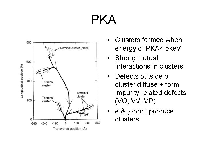
PKA • Clusters formed when energy of PKA< 5 ke. V • Strong mutual interactions in clusters • Defects outside of cluster diffuse + form impurity related defects (VO, VV, VP) • e & don’t produce clusters

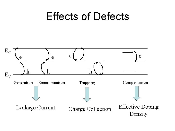
Effects of Defects EC EV e e h Generation h Recombination Leakage Current e e h Trapping Charge Collection Compensation Effective Doping Density

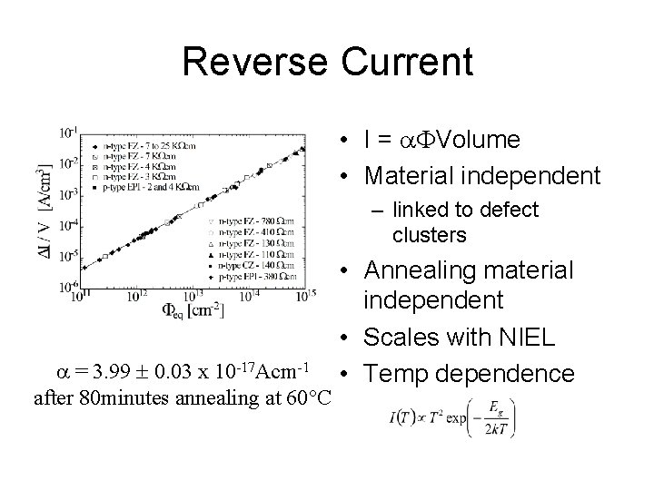
Reverse Current • I = Volume • Material independent – linked to defect clusters = 3. 99 0. 03 x 10 -17 Acm-1 after 80 minutes annealing at 60 C • Annealing material independent • Scales with NIEL • Temp dependence

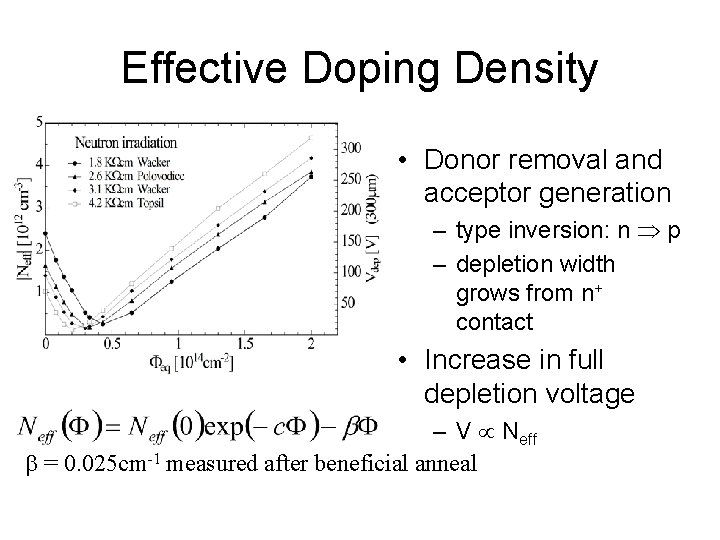
Effective Doping Density • Donor removal and acceptor generation – type inversion: n p – depletion width grows from n+ contact • Increase in full depletion voltage – V Neff = 0. 025 cm-1 measured after beneficial anneal

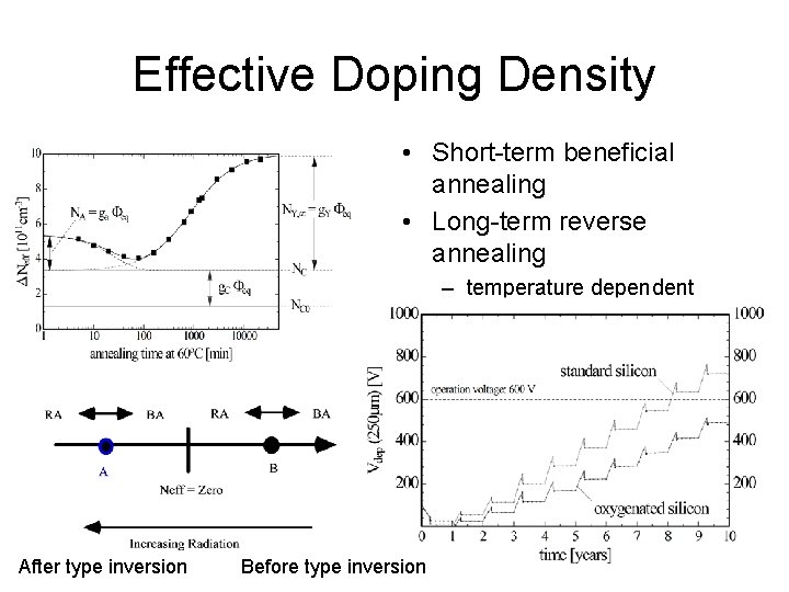
Effective Doping Density • Short-term beneficial annealing • Long-term reverse annealing – temperature dependent – stops below -10 C After type inversion Before type inversion

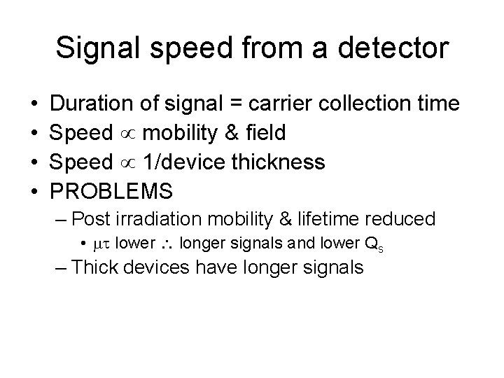
Signal speed from a detector • • Duration of signal = carrier collection time Speed mobility & field Speed 1/device thickness PROBLEMS – Post irradiation mobility & lifetime reduced • lower longer signals and lower Qs – Thick devices have longer signals

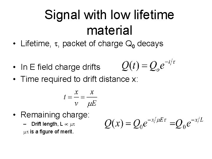
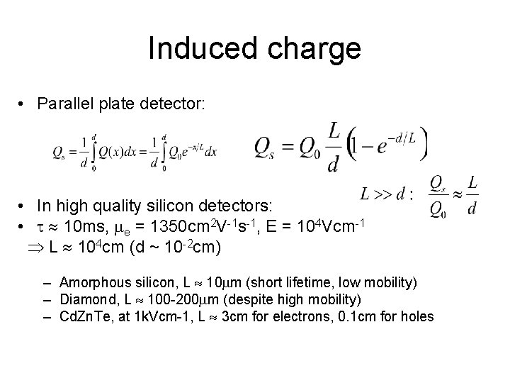
Signal with low lifetime material • Lifetime, , packet of charge Q 0 decays • In E field charge drifts • Time required to drift distance x: • Remaining charge: – Drift length, L is a figure of merit.

Induced charge • Parallel plate detector: • In high quality silicon detectors: • 10 ms, e = 1350 cm 2 V-1 s-1, E = 104 Vcm-1 L 104 cm (d ~ 10 -2 cm) – Amorphous silicon, L 10 m (short lifetime, low mobility) – Diamond, L 100 -200 m (despite high mobility) – Cd. Zn. Te, at 1 k. Vcm-1, L 3 cm for electrons, 0. 1 cm for holes

What can we do? • • Detector Design Material Engineering Cold Operation Electrode Structure – 3 -D device

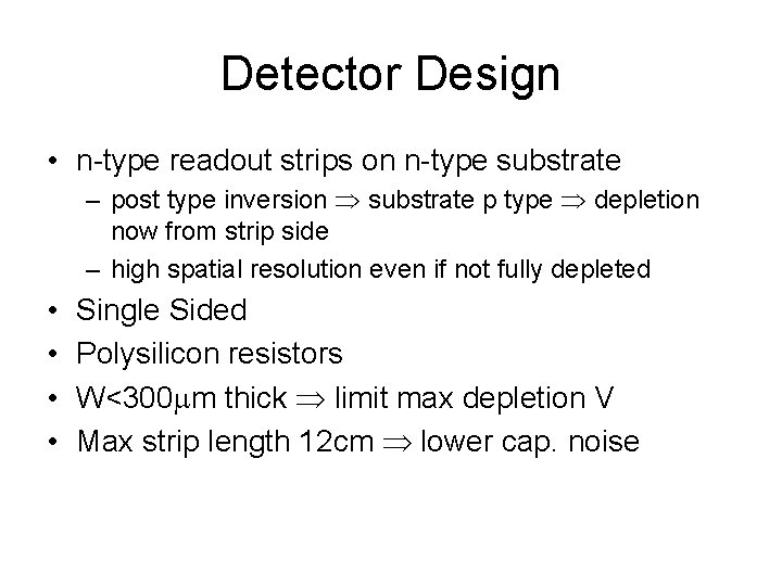
Detector Design • n-type readout strips on n-type substrate – post type inversion substrate p type depletion now from strip side – high spatial resolution even if not fully depleted • • Single Sided Polysilicon resistors W<300 m thick limit max depletion V Max strip length 12 cm lower cap. noise

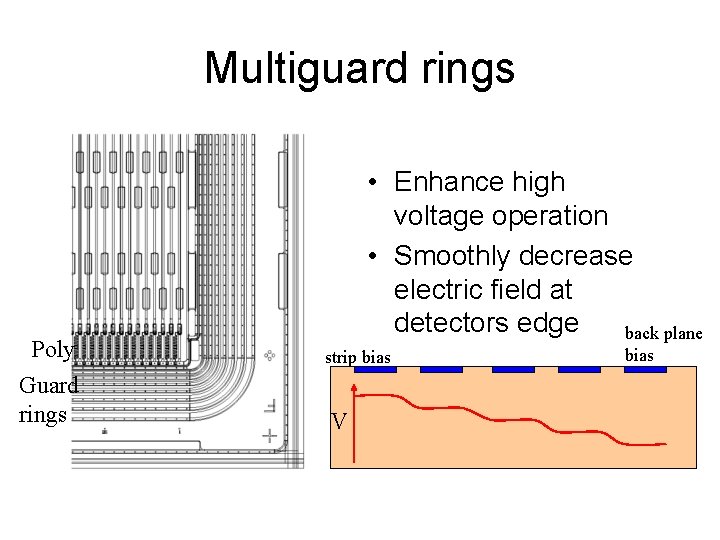
Multiguard rings Poly Guard rings • Enhance high voltage operation • Smoothly decrease electric field at detectors edge back plane strip bias V bias

Substrate Choice • Minimise interface states • Substrate orientation <100> not <111> – Lower capacitive load – Independent of ionising radiation • <100> has less dangling surface bonds

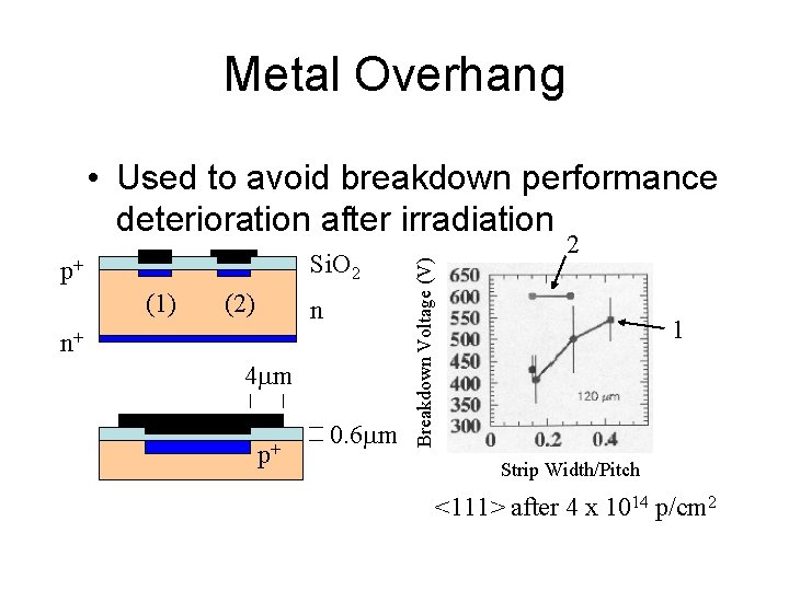
Metal Overhang Si. O 2 p+ (1) (2) n n+ 4 m p+ 0. 6 m Breakdown Voltage (V) • Used to avoid breakdown performance deterioration after irradiation 2 1 Strip Width/Pitch <111> after 4 x 10¹⁴ p/cm 2

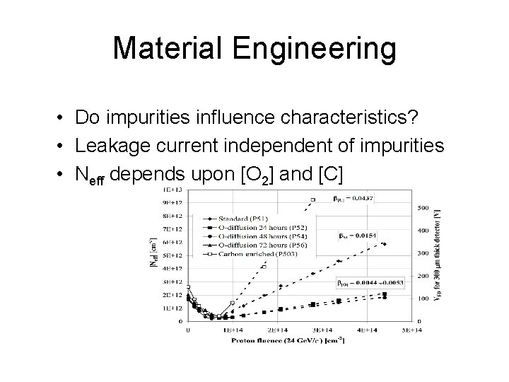
Material Engineering • Do impurities influence characteristics? • Leakage current independent of impurities • Neff depends upon [O 2] and [C]

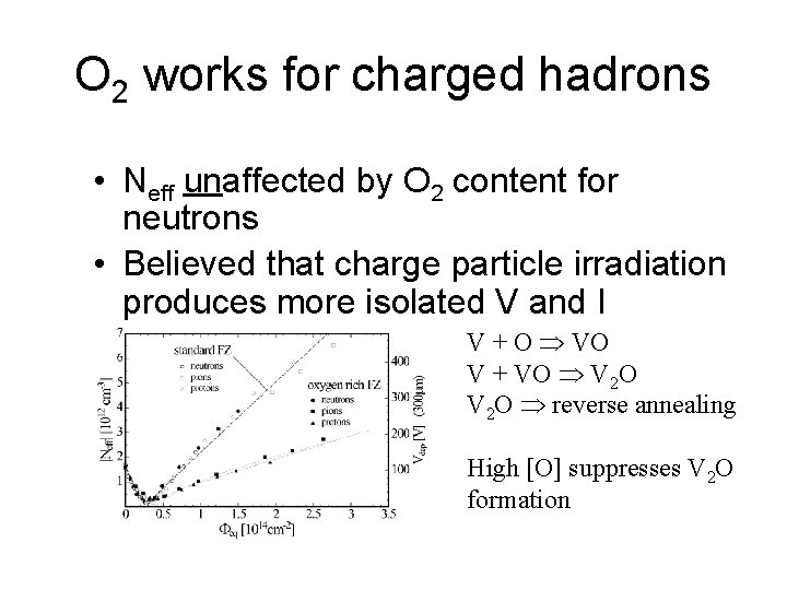
O 2 works for charged hadrons • Neff unaffected by O 2 content for neutrons • Believed that charge particle irradiation produces more isolated V and I V + O VO V + VO V 2 O reverse annealing High [O] suppresses V 2 O formation

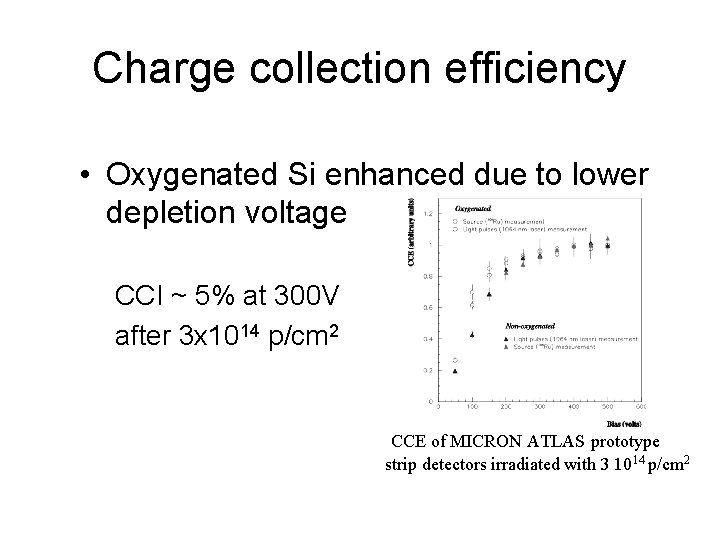
Charge collection efficiency • Oxygenated Si enhanced due to lower depletion voltage CCI ~ 5% at 300 V after 3 x 10¹⁴ p/cm 2 CCE of MICRON ATLAS prototype strip detectors irradiated with 3 1014 p/cm 2

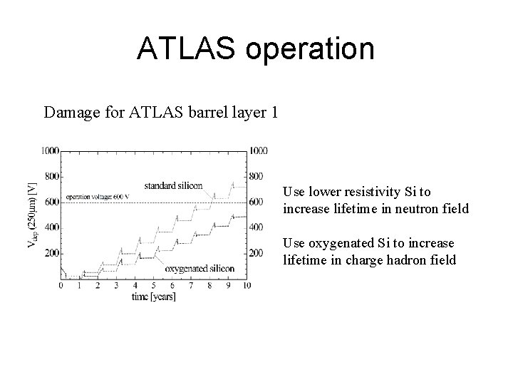
ATLAS operation Damage for ATLAS barrel layer 1 Use lower resistivity Si to increase lifetime in neutron field Use oxygenated Si to increase lifetime in charge hadron field

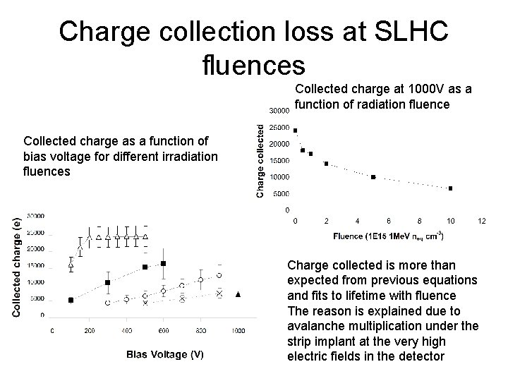
Charge collection loss at SLHC fluences Collected charge at 1000 V as a function of radiation fluence Collected charge as a function of bias voltage for different irradiation fluences Charge collected is more than expected from previous equations and fits to lifetime with fluence The reason is explained due to avalanche multiplication under the strip implant at the very high electric fields in the detector

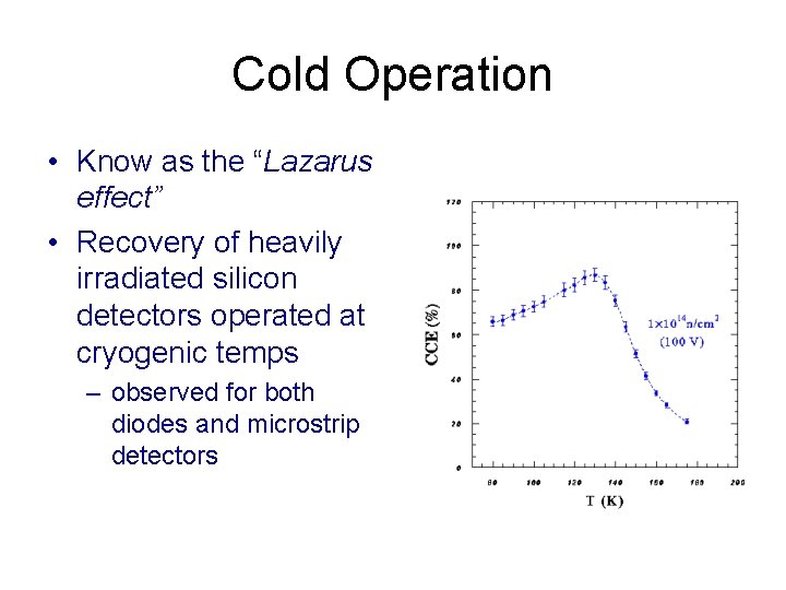
Cold Operation • Know as the “Lazarus effect” • Recovery of heavily irradiated silicon detectors operated at cryogenic temps – observed for both diodes and microstrip detectors

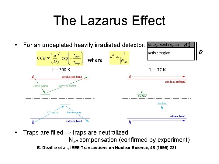
The Lazarus Effect • For an undepleted heavily irradiated detector: undepleted region d active region where • Traps are filled traps are neutralized Neff compensation (confirmed by experiment) B. Dezillie et al. , IEEE Transactions on Nuclear Science, 46 (1999) 221 D

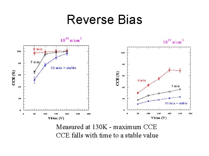
Reverse Bias Measured at 130 K - maximum CCE falls with time to a stable value

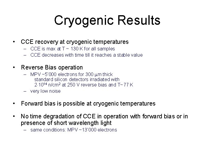
Cryogenic Results • CCE recovery at cryogenic temperatures – CCE is max at T ~ 130 K for all samples – CCE decreases with time till it reaches a stable value • Reverse Bias operation – MPV ~5’ 000 electrons for 300 m thick standard silicon detectors irradiated with 2 1014 n/cm 2 at 250 V reverse bias and T~77 K – very low noise • Forward bias is possible at cryogenic temperatures • No time degradation of CCE in operation with forward bias or in presence of short wavelength light – same conditions: MPV ~13’ 000 electrons

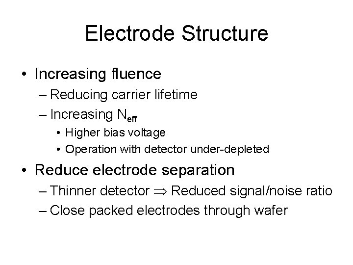
Electrode Structure • Increasing fluence – Reducing carrier lifetime – Increasing Neff • Higher bias voltage • Operation with detector under-depleted • Reduce electrode separation – Thinner detector Reduced signal/noise ratio – Close packed electrodes through wafer

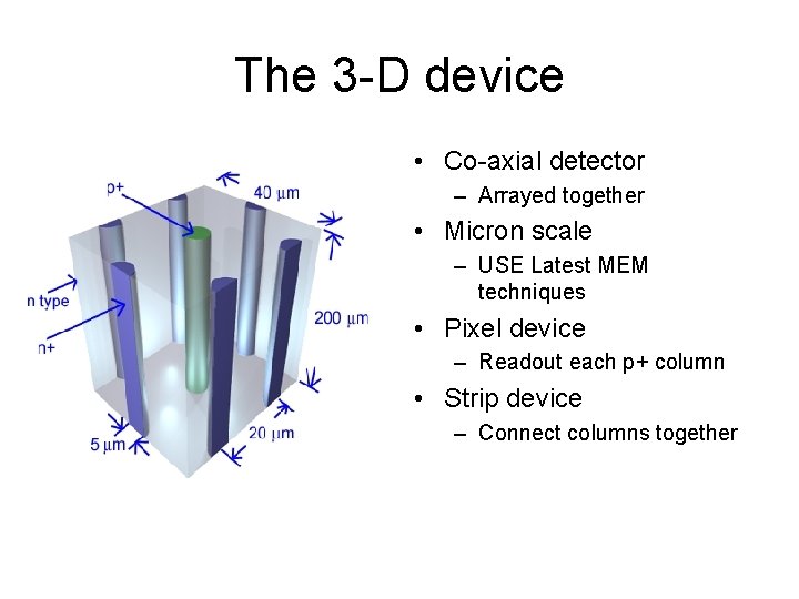
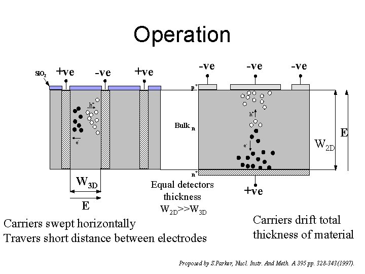
The 3 -D device • Co-axial detector – Arrayed together • Micron scale – USE Latest MEM techniques • Pixel device – Readout each p+ column • Strip device – Connect columns together

Operation Si. O 2 +ve -ve -ve p+ h+ h+ Bulk n e- W 3 D W 2 D e- E n+ Equal detectors thickness W 2 D>>W 3 D E Carriers swept horizontally Travers short distance between electrodes +ve Carriers drift total thickness of material Proposed by S. Parker, Nucl. Instr. And Meth. A 395 pp. 328 -343(1997).

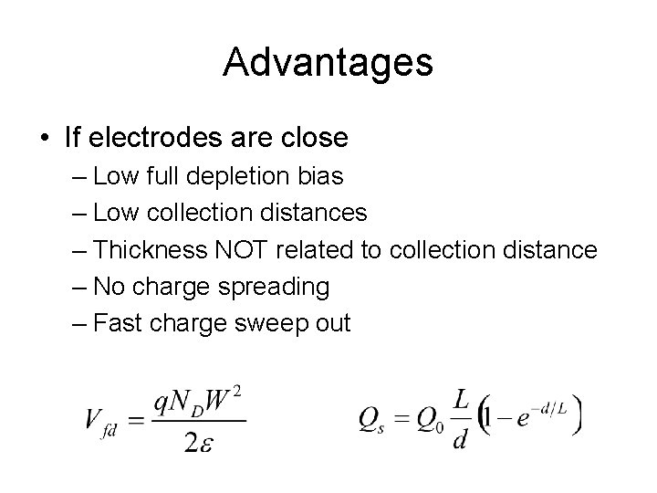
Advantages • If electrodes are close – Low full depletion bias – Low collection distances – Thickness NOT related to collection distance – No charge spreading – Fast charge sweep out

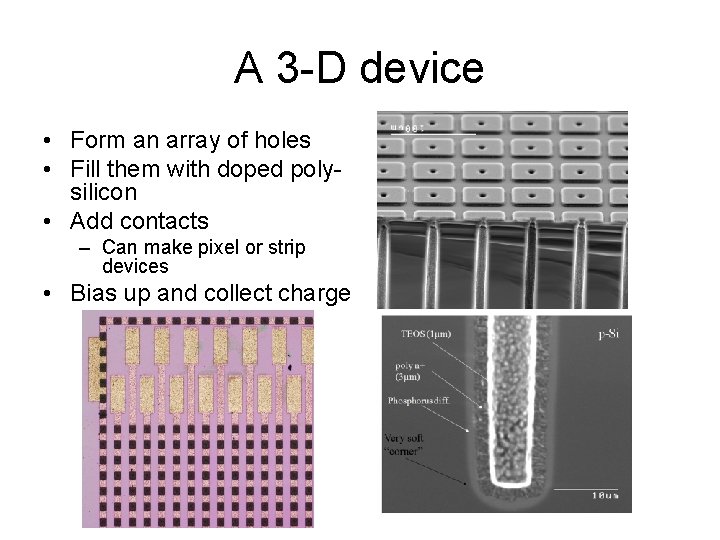
A 3 -D device • Form an array of holes • Fill them with doped polysilicon • Add contacts – Can make pixel or strip devices • Bias up and collect charge

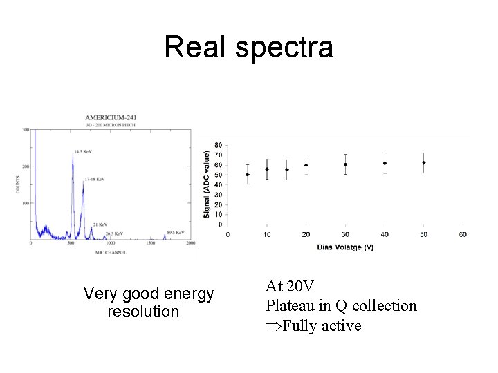
Real spectra Very good energy resolution At 20 V Plateau in Q collection Fully active

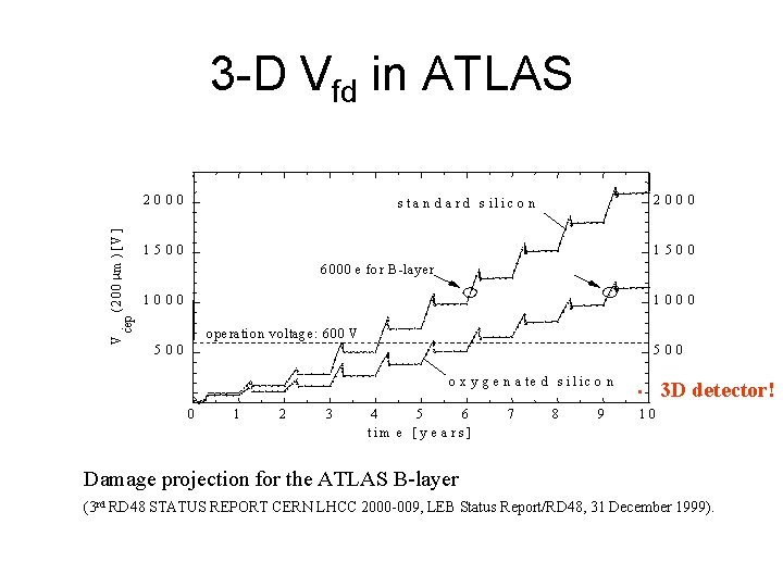
3 -D Vfd in ATLAS V 2000 s ta n d a rd s ilic o n 1500 6 000 e fo r B -lay er 1000 dep (2 00 m ) [V ] 2000 opera tio n voltag e: 60 0 V 500 o x y g e n a te d s ilic o n 0 1 2 3 4 5 6 tim e [y e a rs ] 7 8 9 • 3 D detector! 10 Damage projection for the ATLAS B-layer (3 rd RD 48 STATUS REPORT CERN LHCC 2000 -009, LEB Status Report/RD 48, 31 December 1999).

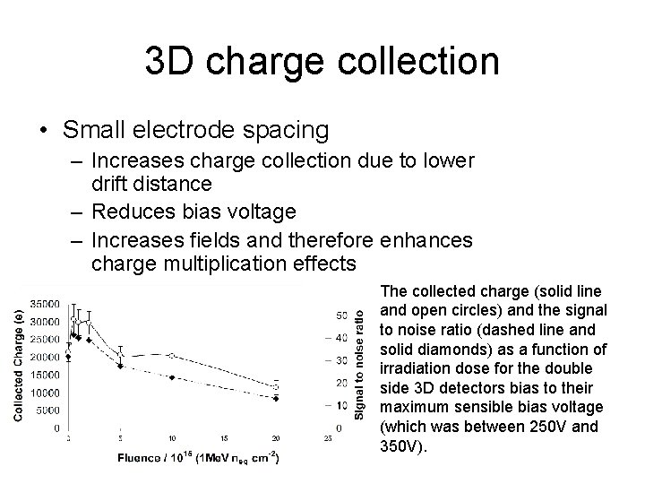
3 D charge collection • Small electrode spacing – Increases charge collection due to lower drift distance – Reduces bias voltage – Increases fields and therefore enhances charge multiplication effects The measured collected charge (solid line fromand 285 open um thick p-type circles) and 3 D the signal detectors operate at a biasline of and to noise ratio (dashed no more than 150 V as (solid line solid diamonds) a function of andirradiation open circles) and dose for 320 the um double thickside p-type planar detectors 3 D detectors bias to their operated at a bias up tobias 1000 V maximum sensible voltage (dashed line and closed 250 V and (which was between diamonds) 350 V). as a function of irradiation dose.

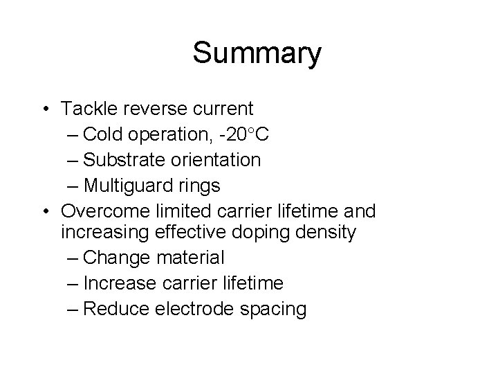
Summary • Tackle reverse current – Cold operation, -20 C – Substrate orientation – Multiguard rings • Overcome limited carrier lifetime and increasing effective doping density – Change material – Increase carrier lifetime – Reduce electrode spacing

Final Slide • • • Why? Where? How? A major type A major worry