Lecture 10 Power Dr Sadr Yazd University Outline
- Slides: 23

Lecture 10: Power Dr. Sadr Yazd University

Outline q Power and Energy q Dynamic Power q Static Power 10: Power CMOS VLSI Design 4 th Ed. 2

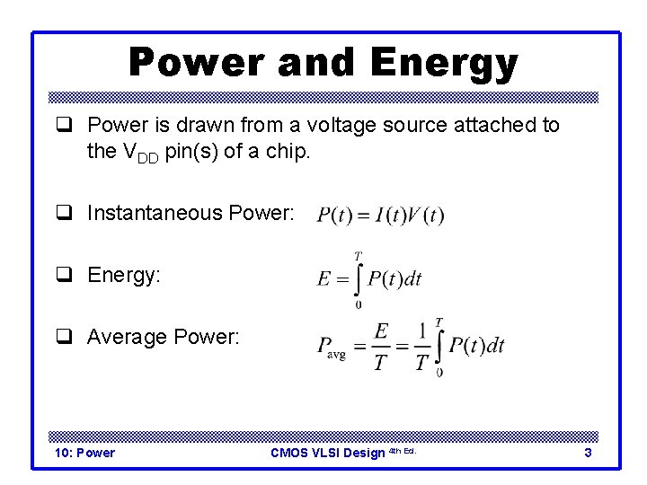
Power and Energy q Power is drawn from a voltage source attached to the VDD pin(s) of a chip. q Instantaneous Power: q Energy: q Average Power: 10: Power CMOS VLSI Design 4 th Ed. 3

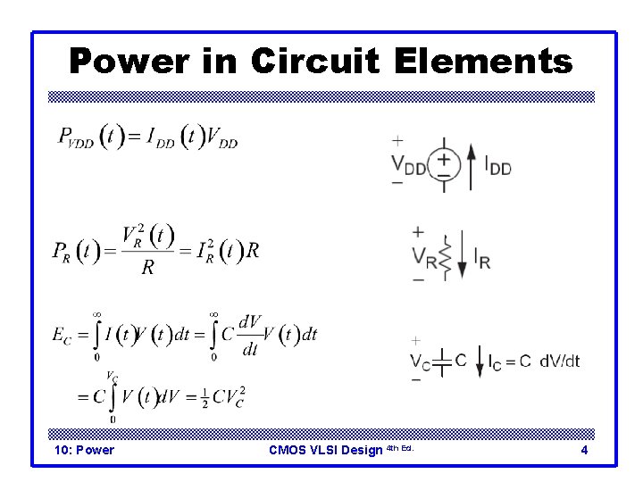
Power in Circuit Elements 10: Power CMOS VLSI Design 4 th Ed. 4

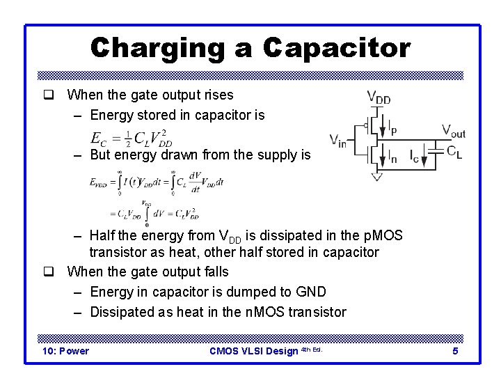
Charging a Capacitor q When the gate output rises – Energy stored in capacitor is – But energy drawn from the supply is – Half the energy from VDD is dissipated in the p. MOS transistor as heat, other half stored in capacitor q When the gate output falls – Energy in capacitor is dumped to GND – Dissipated as heat in the n. MOS transistor 10: Power CMOS VLSI Design 4 th Ed. 5

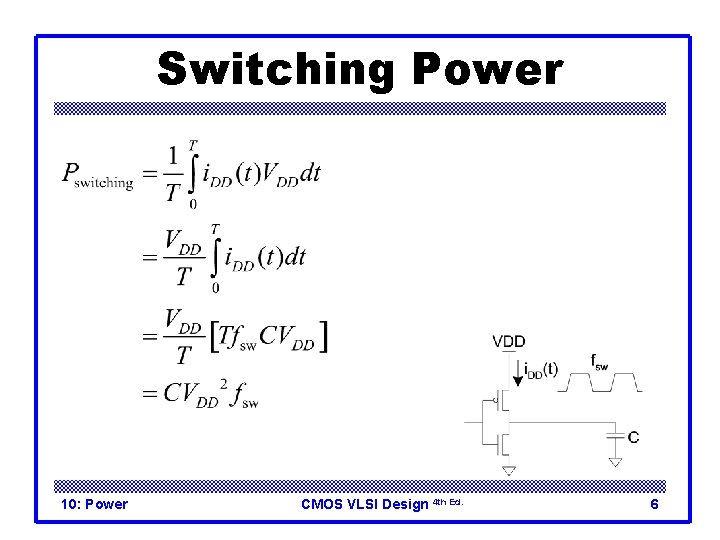
Switching Power 10: Power CMOS VLSI Design 4 th Ed. 6

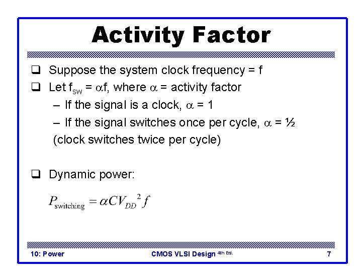
Activity Factor q Suppose the system clock frequency = f q Let fsw = af, where a = activity factor – If the signal is a clock, a = 1 – If the signal switches once per cycle, a = ½ (clock switches twice per cycle) q Dynamic power: 10: Power CMOS VLSI Design 4 th Ed. 7

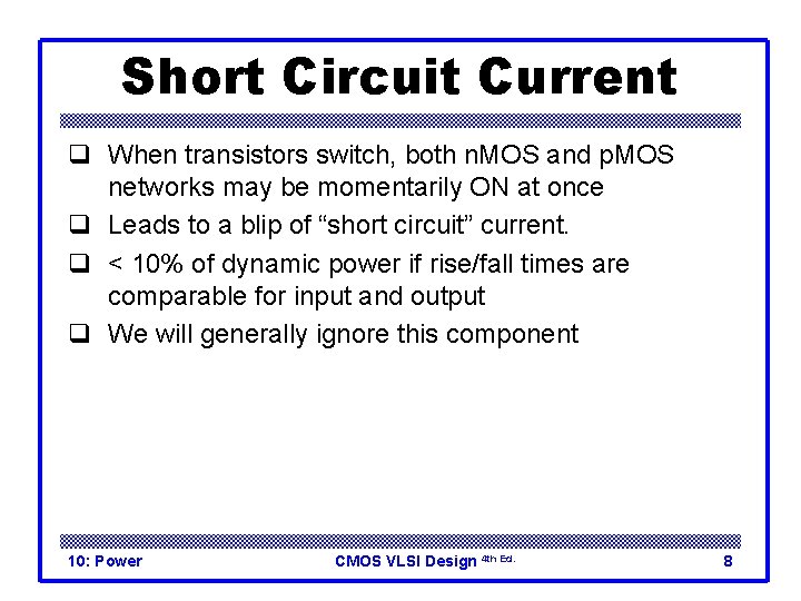
Short Circuit Current q When transistors switch, both n. MOS and p. MOS networks may be momentarily ON at once q Leads to a blip of “short circuit” current. q < 10% of dynamic power if rise/fall times are comparable for input and output q We will generally ignore this component 10: Power CMOS VLSI Design 4 th Ed. 8

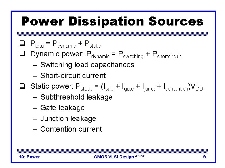
Power Dissipation Sources q Ptotal = Pdynamic + Pstatic q Dynamic power: Pdynamic = Pswitching + Pshortcircuit – Switching load capacitances – Short-circuit current q Static power: Pstatic = (Isub + Igate + Ijunct + Icontention)VDD – Subthreshold leakage – Gate leakage – Junction leakage – Contention current 10: Power CMOS VLSI Design 4 th Ed. 9

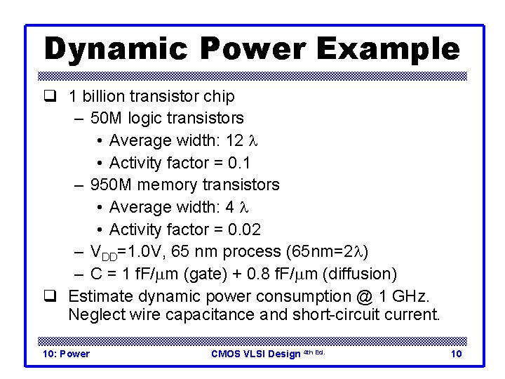
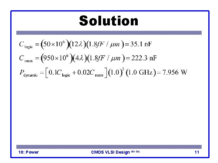
Dynamic Power Example q 1 billion transistor chip – 50 M logic transistors • Average width: 12 l • Activity factor = 0. 1 – 950 M memory transistors • Average width: 4 l • Activity factor = 0. 02 – VDD=1. 0 V, 65 nm process (65 nm=2 l) – C = 1 f. F/mm (gate) + 0. 8 f. F/mm (diffusion) q Estimate dynamic power consumption @ 1 GHz. Neglect wire capacitance and short-circuit current. 10: Power CMOS VLSI Design 4 th Ed. 10

Solution 10: Power CMOS VLSI Design 4 th Ed. 11

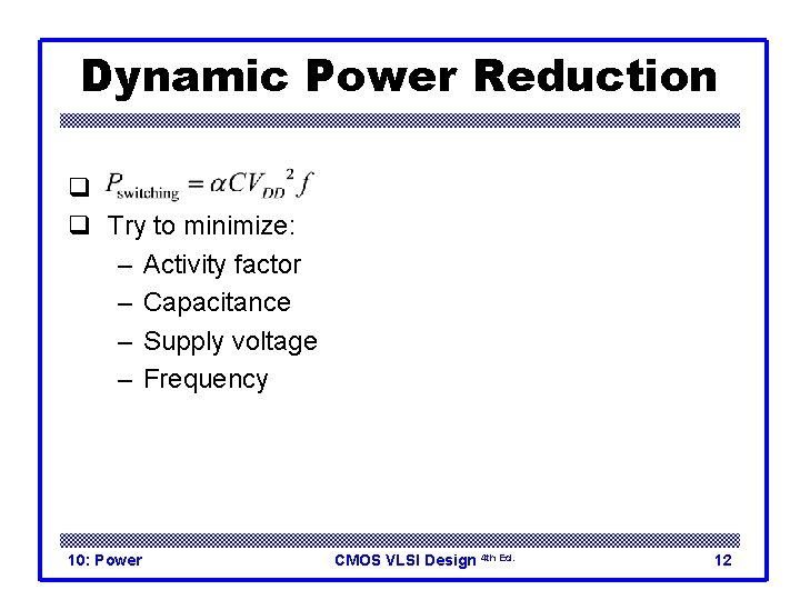
Dynamic Power Reduction q q Try to minimize: – Activity factor – Capacitance – Supply voltage – Frequency 10: Power CMOS VLSI Design 4 th Ed. 12

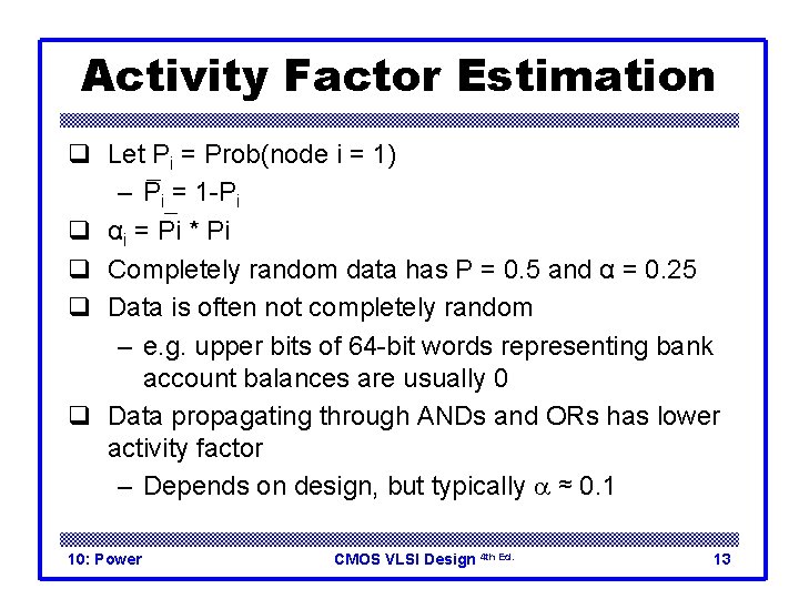
Activity Factor Estimation q Let Pi = Prob(node i = 1) – Pi = 1 -Pi q αi = Pi * Pi q Completely random data has P = 0. 5 and α = 0. 25 q Data is often not completely random – e. g. upper bits of 64 -bit words representing bank account balances are usually 0 q Data propagating through ANDs and ORs has lower activity factor – Depends on design, but typically a ≈ 0. 1 10: Power CMOS VLSI Design 4 th Ed. 13

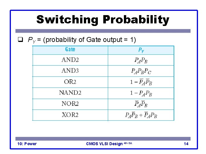
Switching Probability q PY = (probability of Gate output = 1) 10: Power CMOS VLSI Design 4 th Ed. 14

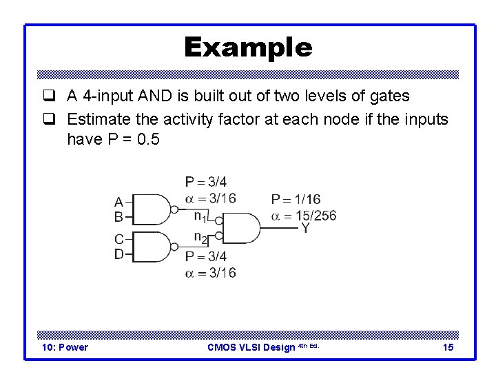
Example q A 4 -input AND is built out of two levels of gates q Estimate the activity factor at each node if the inputs have P = 0. 5 10: Power CMOS VLSI Design 4 th Ed. 15

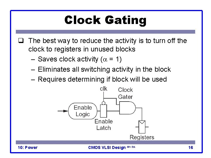
Clock Gating q The best way to reduce the activity is to turn off the clock to registers in unused blocks – Saves clock activity (a = 1) – Eliminates all switching activity in the block – Requires determining if block will be used 10: Power CMOS VLSI Design 4 th Ed. 16

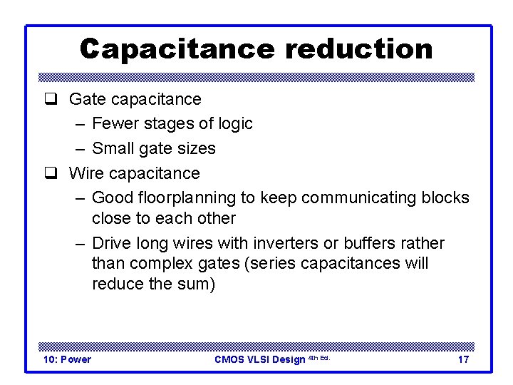
Capacitance reduction q Gate capacitance – Fewer stages of logic – Small gate sizes q Wire capacitance – Good floorplanning to keep communicating blocks close to each other – Drive long wires with inverters or buffers rather than complex gates (series capacitances will reduce the sum) 10: Power CMOS VLSI Design 4 th Ed. 17

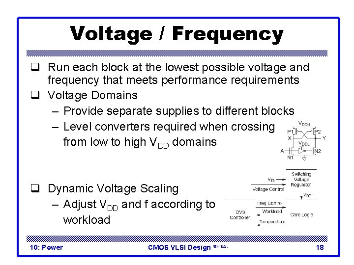
Voltage / Frequency q Run each block at the lowest possible voltage and frequency that meets performance requirements q Voltage Domains – Provide separate supplies to different blocks – Level converters required when crossing from low to high VDD domains q Dynamic Voltage Scaling – Adjust VDD and f according to workload 10: Power CMOS VLSI Design 4 th Ed. 18

Static Power q Static power is consumed even when chip is quiescent. – Leakage draws power from nominally OFF devices – Ratioed circuits burn power in fight between ON transistors 10: Power CMOS VLSI Design 4 th Ed. 19

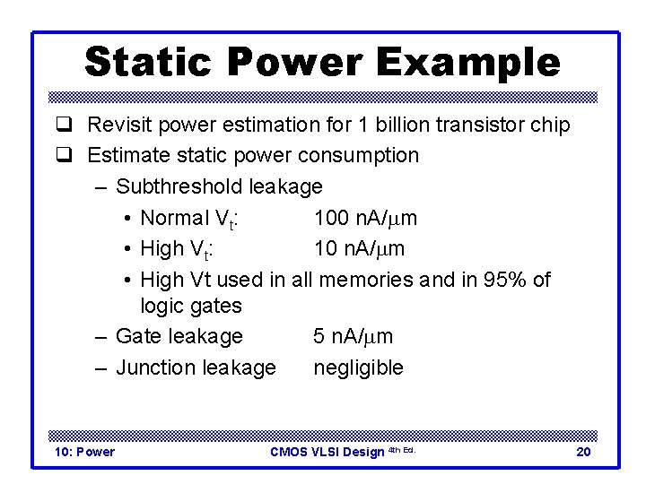
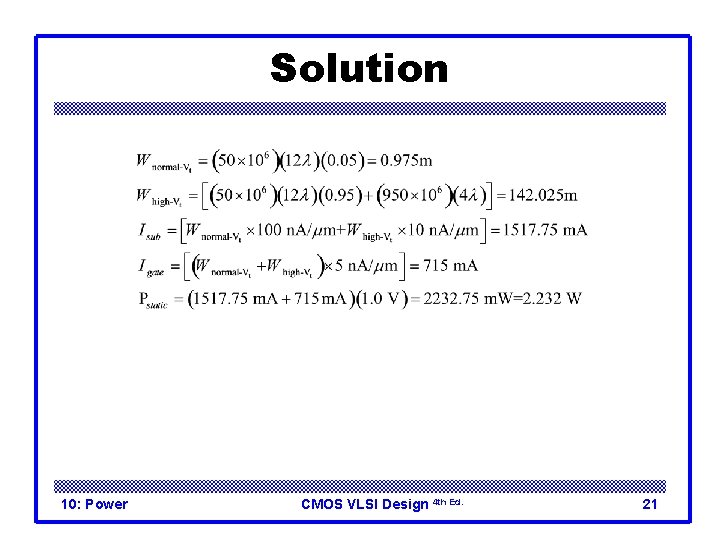
Static Power Example q Revisit power estimation for 1 billion transistor chip q Estimate static power consumption – Subthreshold leakage • Normal Vt: 100 n. A/mm • High Vt: 10 n. A/mm • High Vt used in all memories and in 95% of logic gates – Gate leakage 5 n. A/mm – Junction leakage negligible 10: Power CMOS VLSI Design 4 th Ed. 20

Solution 10: Power CMOS VLSI Design 4 th Ed. 21

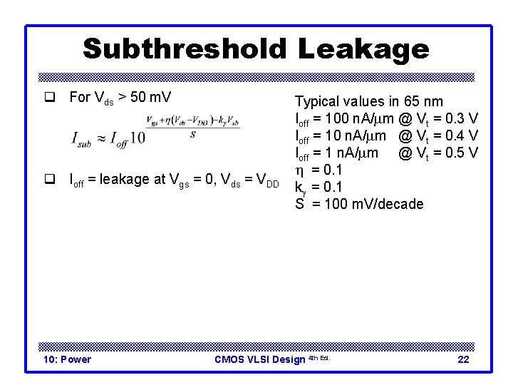
Subthreshold Leakage q For Vds > 50 m. V q Ioff = leakage at Vgs = 0, Vds = VDD 10: Power Typical values in 65 nm Ioff = 100 n. A/mm @ Vt = 0. 3 V Ioff = 10 n. A/mm @ Vt = 0. 4 V Ioff = 1 n. A/mm @ Vt = 0. 5 V h = 0. 1 kg = 0. 1 S = 100 m. V/decade CMOS VLSI Design 4 th Ed. 22

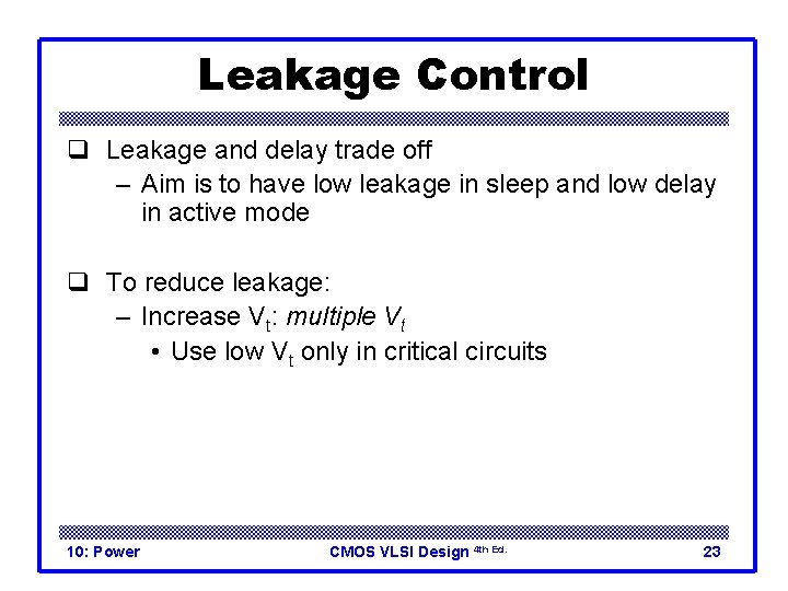
Leakage Control q Leakage and delay trade off – Aim is to have low leakage in sleep and low delay in active mode q To reduce leakage: – Increase Vt: multiple Vt • Use low Vt only in critical circuits 10: Power CMOS VLSI Design 4 th Ed. 23