Glow Discharge Optical Spectrometry GD OES Principles and

- Slides: 49

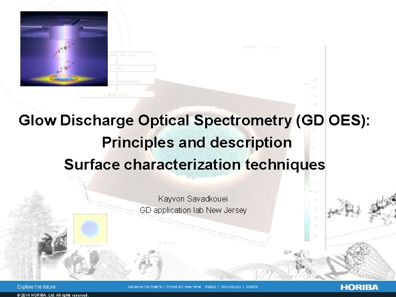
Glow Discharge Optical Spectrometry (GD OES): Principles and description Surface characterization techniques Kayvon Savadkouei GD application lab New Jersey © 2014 HORIBA, Ltd. All rights reserved.

Topics n Principles of the technique n GD-OES vs other surface analysis techniques l SEM l XPS l Various n Conclusions © 2014 HORIBA, Ltd. All rights reserved.

Main features Characteristics of pulsed RF GD-OES instruments n All elements of periodic table (incl. H, O, N, C) n Fast sputtering (2 -150 nm/s) n Depth Profile n Thin and thick films (nm to 200µm) n Isotopic information for Deuterium n Depth resolution (nm scale) © 2014 HORIBA, Ltd. All rights reserved.

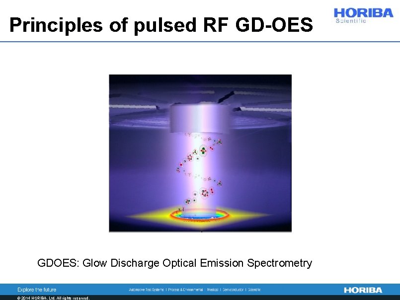
Principles of pulsed RF GD-OES GDOES: Glow Discharge Optical Emission Spectrometry © 2014 HORIBA, Ltd. All rights reserved.

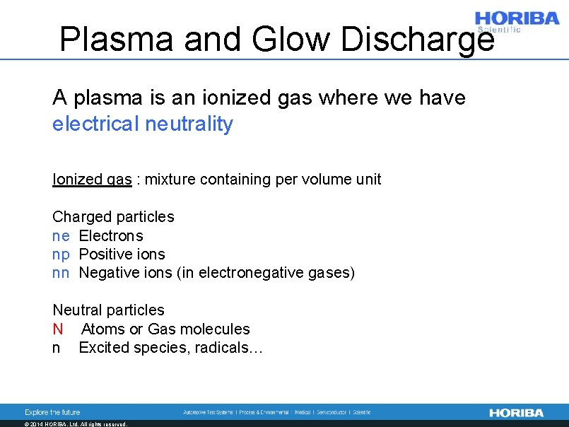
Plasma and Glow Discharge A plasma is an ionized gas where we have electrical neutrality Ionized gas : mixture containing per volume unit Charged particles ne Electrons np Positive ions nn Negative ions (in electronegative gases) Neutral particles N Atoms or Gas molecules n Excited species, radicals… © 2014 HORIBA, Ltd. All rights reserved.

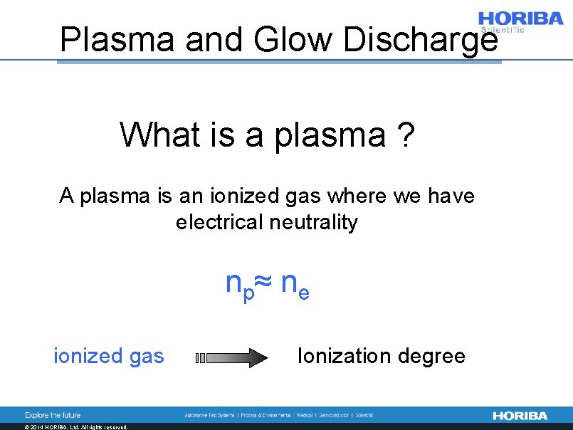
Plasma and Glow Discharge What is a plasma ? A plasma is an ionized gas where we have electrical neutrality n p≈ n e ionized gas © 2014 HORIBA, Ltd. All rights reserved. Ionization degree

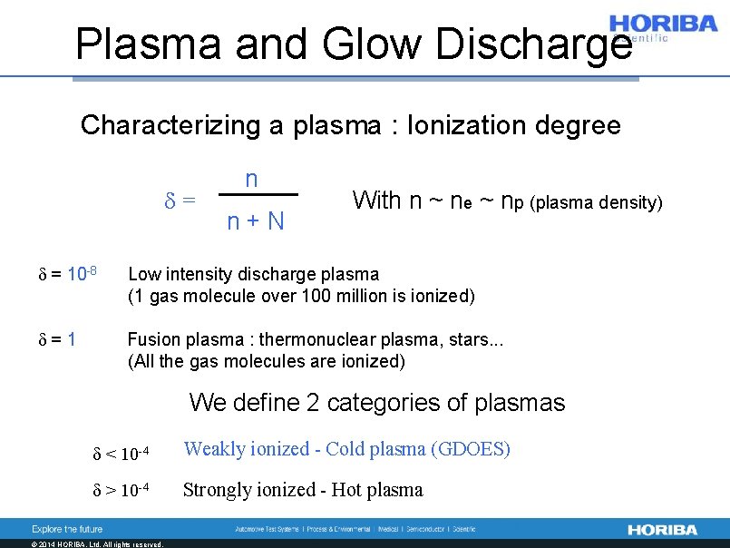
Plasma and Glow Discharge Characterizing a plasma : Ionization degree d= n n+N With n ~ ne ~ np (plasma density) d = 10 -8 Low intensity discharge plasma (1 gas molecule over 100 million is ionized) d=1 Fusion plasma : thermonuclear plasma, stars. . . (All the gas molecules are ionized) We define 2 categories of plasmas d < 10 -4 Weakly ionized - Cold plasma (GDOES) d > 10 -4 Strongly ionized - Hot plasma © 2014 HORIBA, Ltd. All rights reserved.

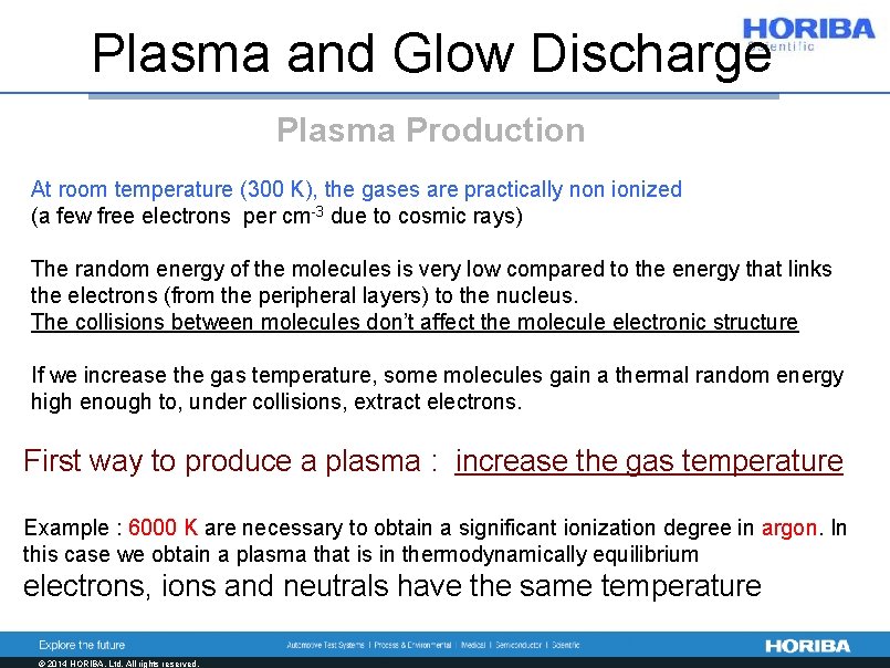
Plasma and Glow Discharge Plasma Production At room temperature (300 K), the gases are practically non ionized (a few free electrons per cm-3 due to cosmic rays) The random energy of the molecules is very low compared to the energy that links the electrons (from the peripheral layers) to the nucleus. The collisions between molecules don’t affect the molecule electronic structure If we increase the gas temperature, some molecules gain a thermal random energy high enough to, under collisions, extract electrons. First way to produce a plasma : increase the gas temperature Example : 6000 K are necessary to obtain a significant ionization degree in argon. In this case we obtain a plasma that is in thermodynamically equilibrium electrons, ions and neutrals have the same temperature © 2014 HORIBA, Ltd. All rights reserved.

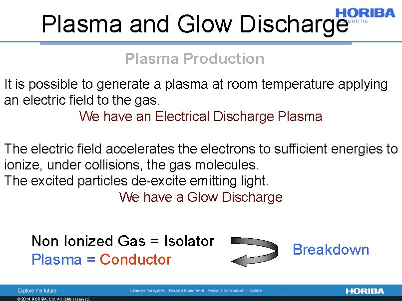
Plasma and Glow Discharge Plasma Production It is possible to generate a plasma at room temperature applying an electric field to the gas. We have an Electrical Discharge Plasma The electric field accelerates the electrons to sufficient energies to ionize, under collisions, the gas molecules. The excited particles de-excite emitting light. We have a Glow Discharge Non Ionized Gas = Isolator Plasma = Conductor © 2014 HORIBA, Ltd. All rights reserved. Breakdown

Plasma and Glow Discharge GD-OES - What we have : Glow Discharge (spectroscopy) Non Equilibrium Cold Plasma (Te>>Tp>Tg) The electrons do the job Active species at low gas temperature © 2014 HORIBA, Ltd. All rights reserved.

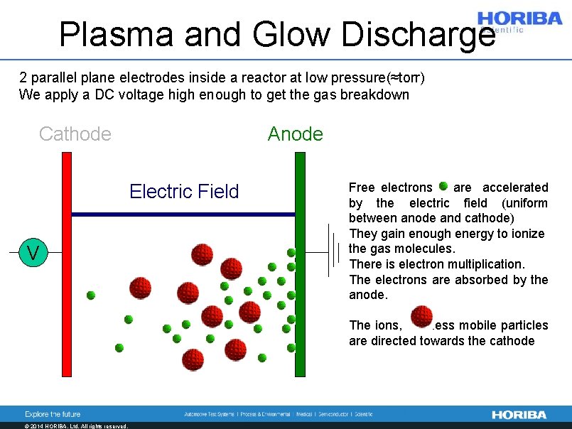
Plasma and Glow Discharge 2 parallel plane electrodes inside a reactor at low pressure(≈torr) We apply a DC voltage high enough to get the gas breakdown Cathode Anode Electric Field V Free electrons are accelerated by the electric field (uniform between anode and cathode) They gain enough energy to ionize the gas molecules. There is electron multiplication. The electrons are absorbed by the anode. The ions, less mobile particles are directed towards the cathode © 2014 HORIBA, Ltd. All rights reserved.

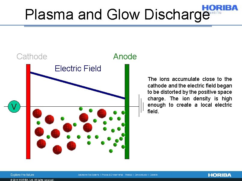
Plasma and Glow Discharge Cathode Anode Electric Field V © 2014 HORIBA, Ltd. All rights reserved. The ions accumulate close to the cathode and the electric field began to be distorted by the positive space charge. The ion density is high enough to create a local electric field.

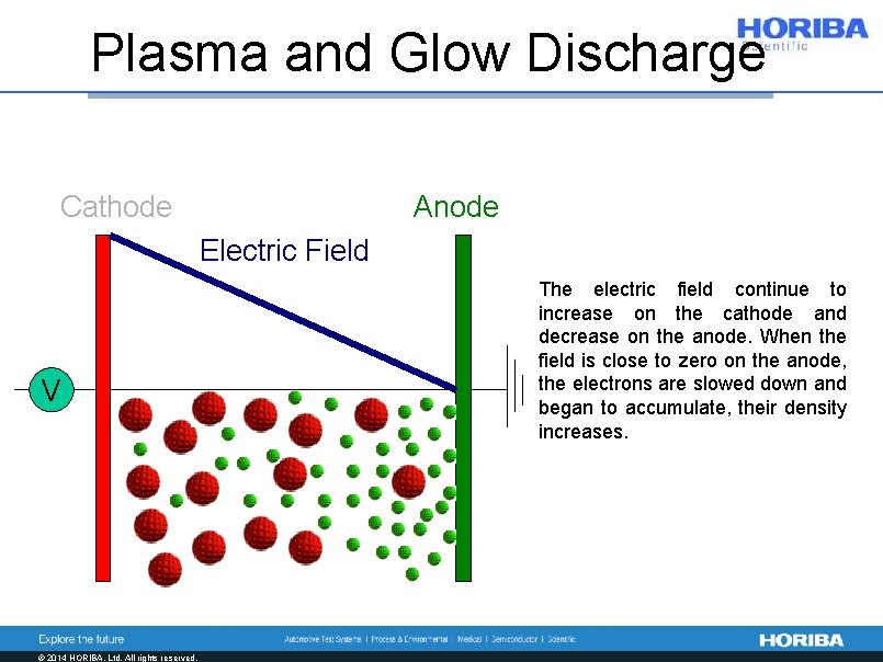
Plasma and Glow Discharge Cathode Anode Electric Field V © 2014 HORIBA, Ltd. All rights reserved. The electric field continue to increase on the cathode and decrease on the anode. When the field is close to zero on the anode, the electrons are slowed down and began to accumulate, their density increases.

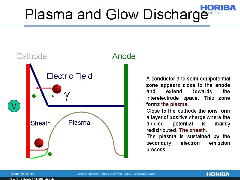
Plasma and Glow Discharge Cathode Anode Electric Field g V Sheath © 2014 HORIBA, Ltd. All rights reserved. Plasma A conductor and semi equipotential zone appears close to the anode and extend towards the interelectrode space. This zone forms the plasma. Close to the cathode the ions form a layer of positive charge where the applied potential is mainly redistributed. The sheath. The plasma is sustained by the secondary electron emission process.

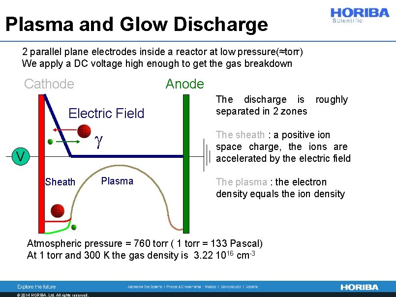
Plasma and Glow Discharge 2 parallel plane electrodes inside a reactor at low pressure(≈torr) We apply a DC voltage high enough to get the gas breakdown Cathode Anode Electric Field g V Sheath Plasma The discharge is roughly separated in 2 zones The sheath : a positive ion space charge, the ions are accelerated by the electric field The plasma : the electron density equals the ion density Atmospheric pressure = 760 torr ( 1 torr = 133 Pascal) At 1 torr and 300 K the gas density is 3. 22 1016 cm-3 © 2014 HORIBA, Ltd. All rights reserved.

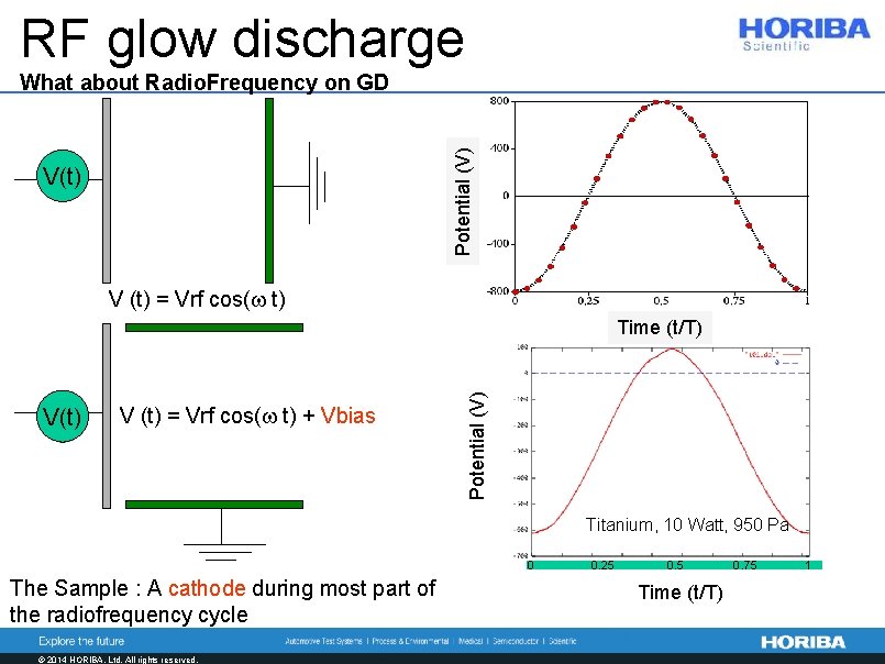
RF glow discharge Potential (V) What about Radio. Frequency on GD V(t) V (t) = Vrf cos(w t) + Vbias Potential (V) Time (t/T) Titanium, 10 Watt, 950 Pa 0 The Sample : A cathode during most part of the radiofrequency cycle © 2014 HORIBA, Ltd. All rights reserved. 0. 25 0. 5 Time (t/T) 0. 75 1

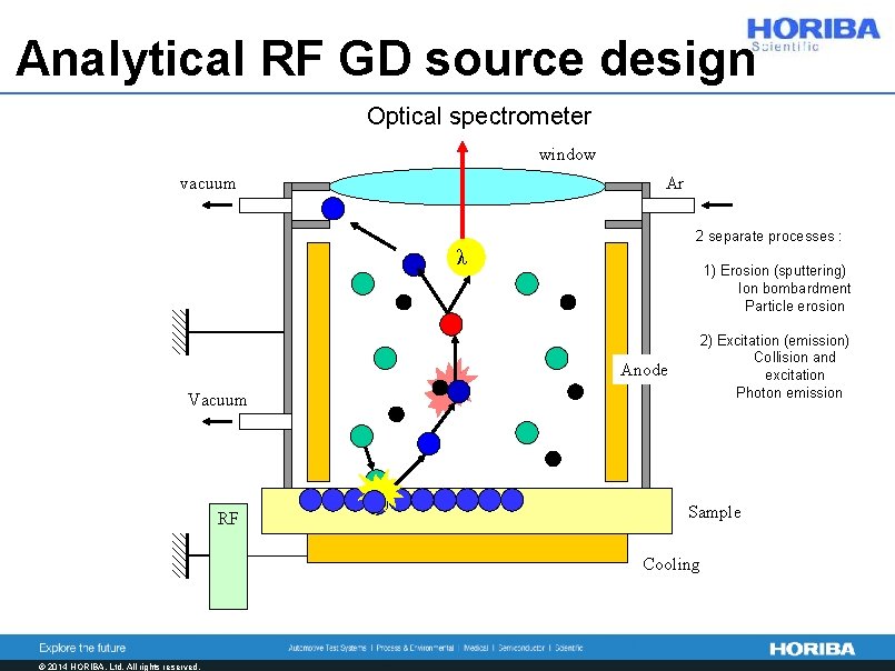
Analytical RF GD source design Optical spectrometer window vacuum Ar 2 separate processes : λ 1) Erosion (sputtering) Ion bombardment Particle erosion Anode Vacuum RF 2) Excitation (emission) Collision and excitation Photon emission Sample Cooling © 2014 HORIBA, Ltd. All rights reserved.

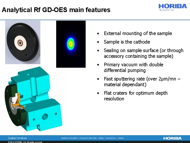
Analytical Rf GD-OES main features © 2014 HORIBA, Ltd. All rights reserved. • External mounting of the sample • Sample is the cathode • Sealing on sample surface (or through accessory containing the sample) • Primary vacuum with double differential pumping • Fast sputtering rate (over 2µm/mn – material dependant) • Flat craters for optimum depth resolution

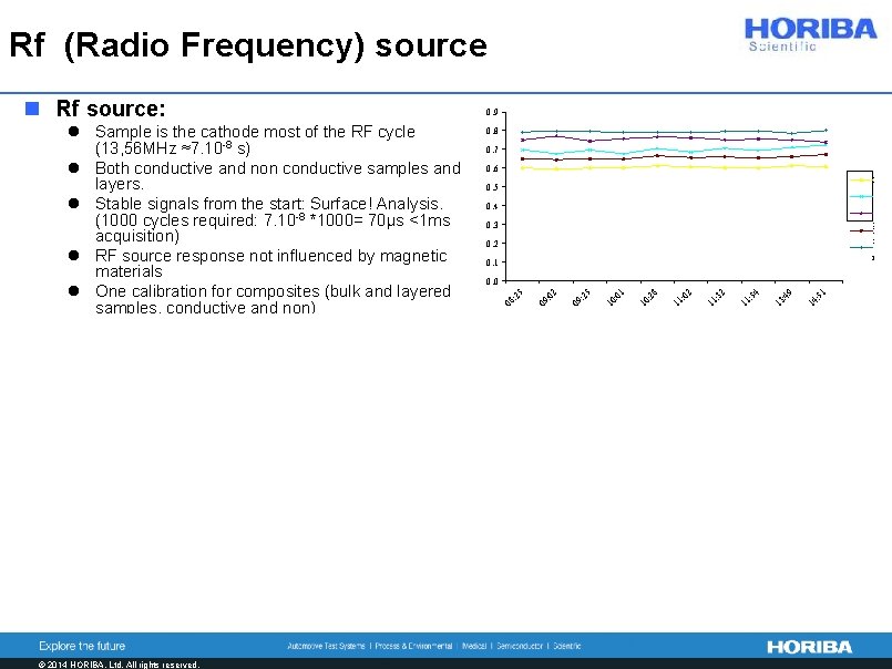
Rf (Radio Frequency) source 0. 8 0. 7 0. 6 P 0. 5 S 0. 4 S i N i C r 0. 3 0. 2 0. 1 51 14 : 49 13 : 54 11 : 32 11 : 02 11 : 28 10 : 01 10 : 25 09 : 02 0. 0 25 l Sample is the cathode most of the RF cycle (13, 56 MHz ≈7. 10 -8 s) l Both conductive and non conductive samples and layers. l Stable signals from the start: Surface! Analysis. (1000 cycles required: 7. 10 -8 *1000= 70µs <1 ms acquisition) l RF source response not influenced by magnetic materials l One calibration for composites (bulk and layered samples, conductive and non) 0. 9 08 : n Rf source: n Pulsed RF: Limit thermal effects on samples exposed to plasma - Ph. Belenguer, et al. Spectrochim. Acta B 64, 7 (2009) 623641. © 2014 HORIBA, Ltd. All rights reserved. l For fragile layers (Less damage) l No unwanted migration (ex: Na from glass) l For Thermo-sensitive materials (e. g. polymers) l For thin films on thick non conductive substrates (glass) power dissipation l For very thin layers: Tune (lower) erosion rate using duty cycle parameter (pulse width/period): Better depth resolution l Soft sputtering and enhanced excitation

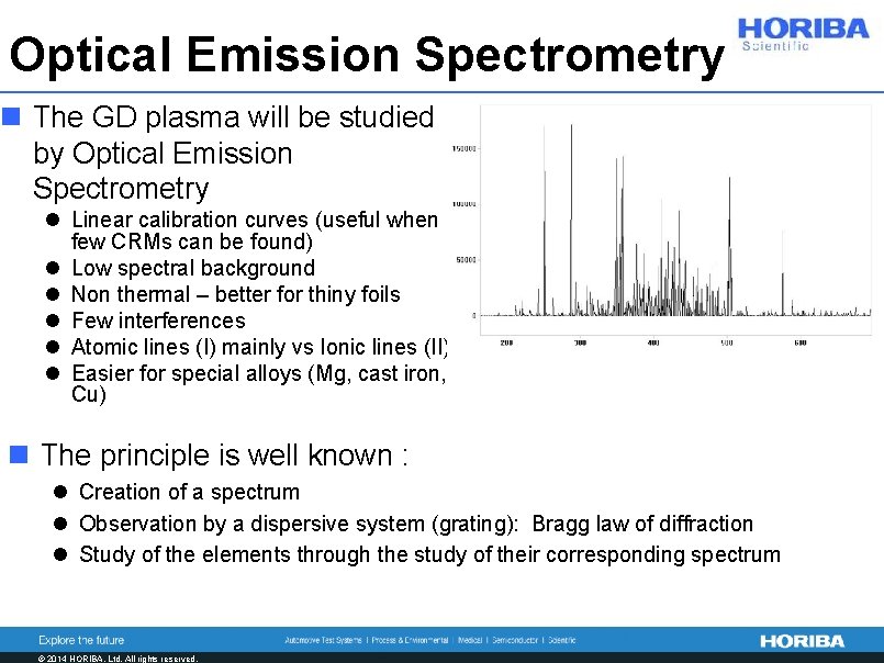
Optical Emission Spectrometry n The GD plasma will be studied by Optical Emission Spectrometry l Linear calibration curves (useful when few CRMs can be found) l Low spectral background l Non thermal – better for thiny foils l Few interferences l Atomic lines (I) mainly vs Ionic lines (II) l Easier for special alloys (Mg, cast iron, Cu) n The principle is well known : l Creation of a spectrum l Observation by a dispersive system (grating): Bragg law of diffraction l Study of the elements through the study of their corresponding spectrum © 2014 HORIBA, Ltd. All rights reserved.

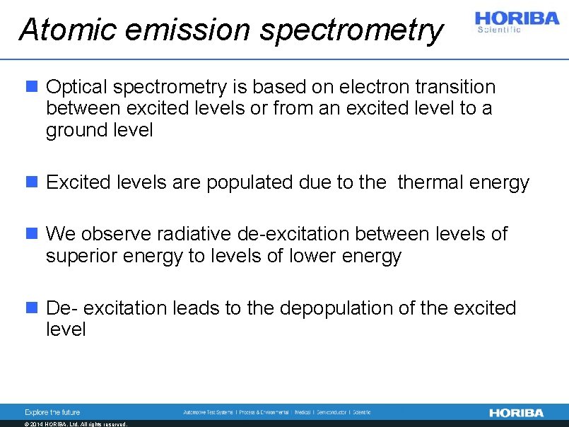
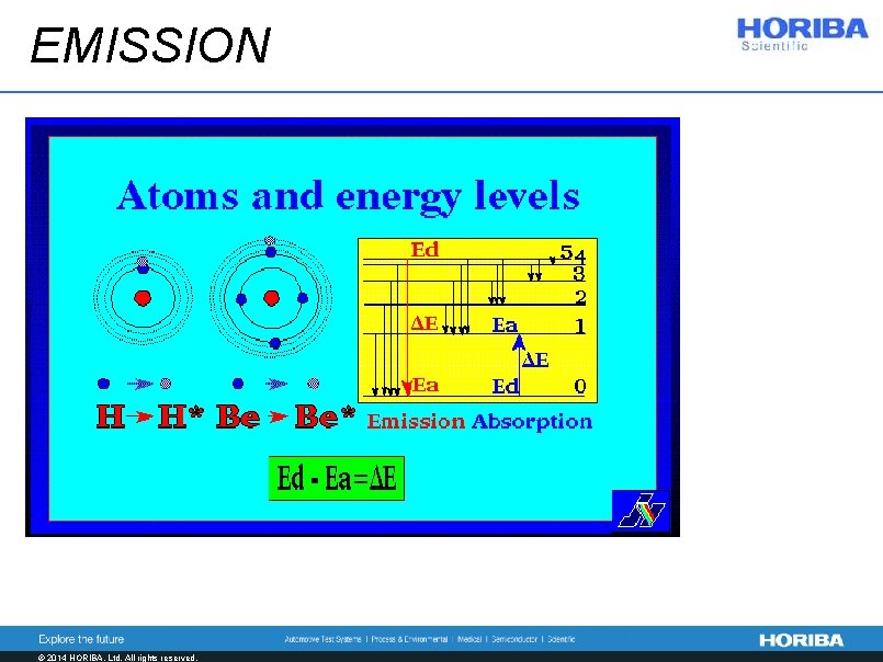
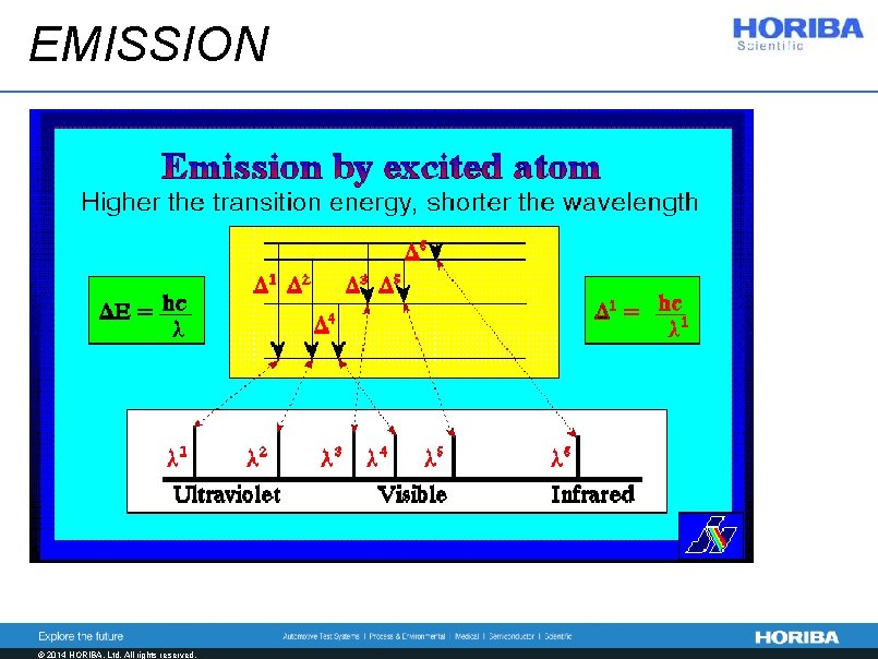
Atomic emission spectrometry n Optical spectrometry is based on electron transition between excited levels or from an excited level to a ground level n Excited levels are populated due to thermal energy n We observe radiative de-excitation between levels of superior energy to levels of lower energy n De- excitation leads to the depopulation of the excited level © 2014 HORIBA, Ltd. All rights reserved.

EMISSION © 2014 HORIBA, Ltd. All rights reserved.

EMISSION © 2014 HORIBA, Ltd. All rights reserved.

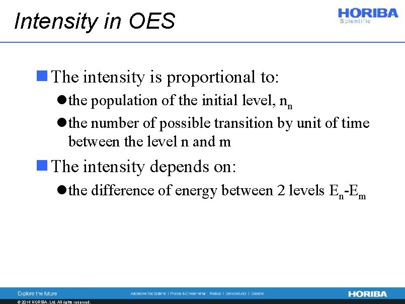
Intensity in OES n The intensity is proportional to: l the population of the initial level, nn l the number of possible transition by unit of time between the level n and m n The intensity depends on: l the difference of energy between 2 levels En-Em © 2014 HORIBA, Ltd. All rights reserved.

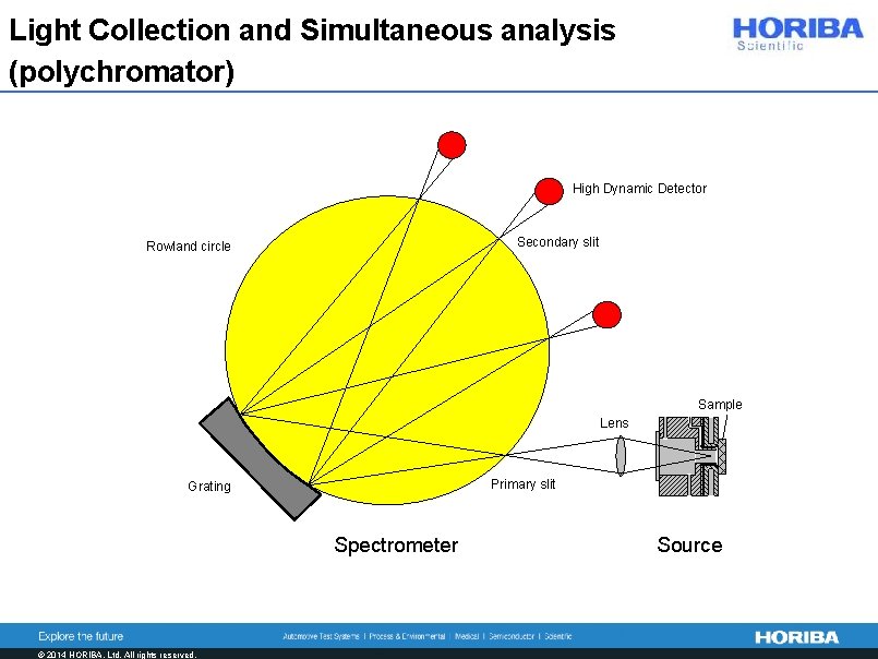
Light Collection and Simultaneous analysis (polychromator) High Dynamic Detector Secondary slit Rowland circle Sample Lens Primary slit Grating Spectrometer © 2014 HORIBA, Ltd. All rights reserved. Source

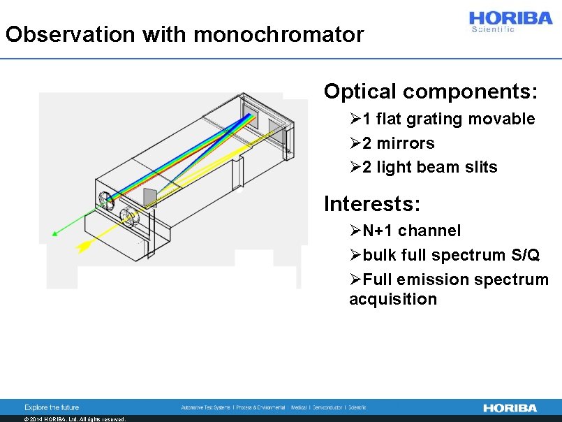
Observation with monochromator Optical components: Ø 1 flat grating movable Ø 2 mirrors Ø 2 light beam slits Interests: ØN+1 channel Øbulk full spectrum S/Q ØFull emission spectrum acquisition © 2014 HORIBA, Ltd. All rights reserved.

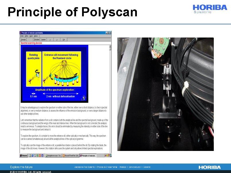
Principle of Polyscan © 2014 HORIBA, Ltd. All rights reserved.

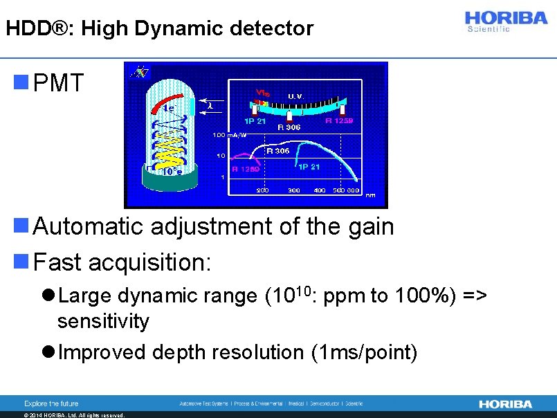
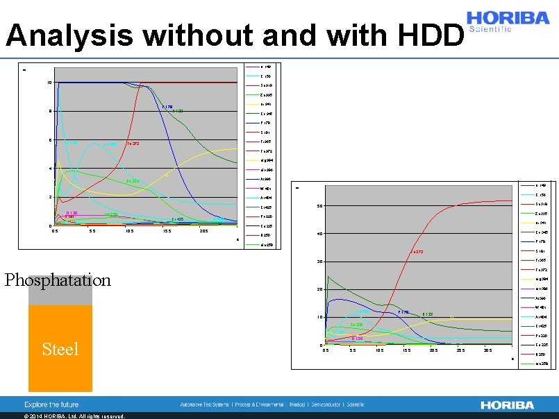
HDD®: High Dynamic detector n PMT n Automatic adjustment of the gain n Fast acquisition: l Large dynamic range (1010: ppm to 100%) => sensitivity l Improved depth resolution (1 ms/point) © 2014 HORIBA, Ltd. All rights reserved.

Analysis without and with HDD H 122 O 130 Cl 135 Si 288 U N 149 C 156 10 Sn 318 Zn 335 Ni 341 P 178 H 122 8 Co 345 P 178 S 181 6 C 156 Na 590 Ti 365 Fe 372 H 122 Fe 372 O 130 Mg 384 4 Cl 135 Mo 386 Fi Si 288 Al 396 W 401 2 N 149 U Zn 335 C 156 Ar 404 Cr 425 O 130 S 181 Mn 258 Cr 425 Sn 318 50 Zn 335 Pb 220 Ar 404 0 Ni 341 Cu 225 0. 5 5. 5 10. 5 15. 5 20. 5 s B 250 Co 345 40 P 178 Mn 258 F 690 Phosphatation S 181 Fe 372 Na 590 Ti 365 30 Fe 372 K 766 Mg 384 Fi Mo 386 20 Al 396 W 401 Na 590 P 178 10 H 122 Fi Ar 404 Zn 335 Cr 425 C 156 Steel Pb 220 O 130 Cu 225 0 0. 5 5. 5 10. 5 15. 5 20. 5 25. 5 30. 5 s B 250 Mn 258 Na 590 F 690 K 766 Fi © 2014 HORIBA, Ltd. All rights reserved.

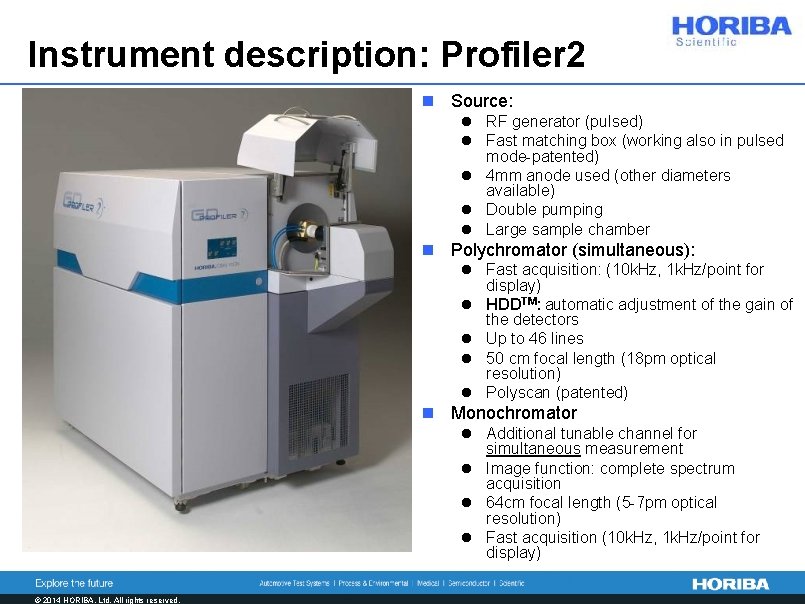
Instrument description: Profiler 2 n Source: l RF generator (pulsed) l Fast matching box (working also in pulsed mode-patented) l 4 mm anode used (other diameters available) l Double pumping l Large sample chamber n Polychromator (simultaneous): l Fast acquisition: (10 k. Hz, 1 k. Hz/point for display) l HDDTM: automatic adjustment of the gain of the detectors l Up to 46 lines l 50 cm focal length (18 pm optical resolution) l Polyscan (patented) n Monochromator l Additional tunable channel for simultaneous measurement l Image function: complete spectrum acquisition l 64 cm focal length (5 -7 pm optical resolution) l Fast acquisition (10 k. Hz, 1 k. Hz/point for display) © 2014 HORIBA, Ltd. All rights reserved.

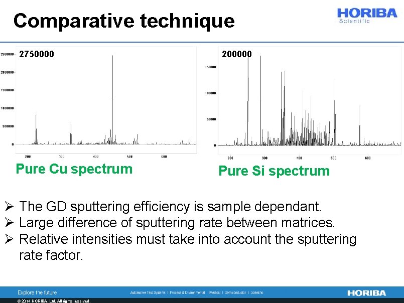
Comparative technique 2750000 Pure Cu spectrum 200000 Pure Si spectrum Ø The GD sputtering efficiency is sample dependant. Ø Large difference of sputtering rate between matrices. Ø Relative intensities must take into account the sputtering rate factor. © 2014 HORIBA, Ltd. All rights reserved.

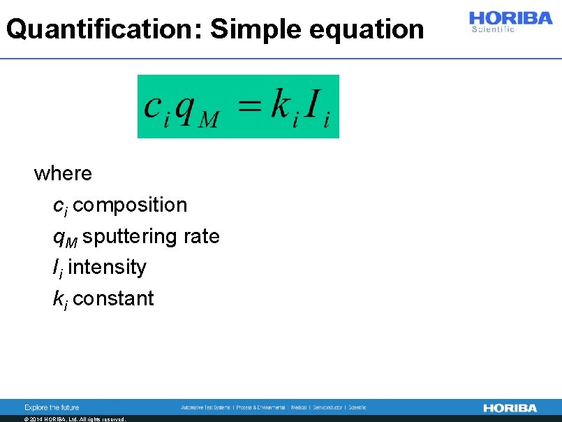
Quantification: Simple equation where – ci composition – q. M sputtering rate – Ii intensity – ki constant © 2014 HORIBA, Ltd. All rights reserved.

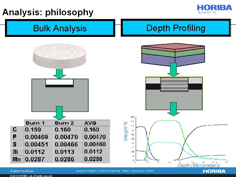
Analysis: philosophy Depth Profiling Weight % Bulk Analysis Cr Ni Fe Px 5 N Cr Depth (Micrometers) © 2014 HORIBA, Ltd. All rights reserved.

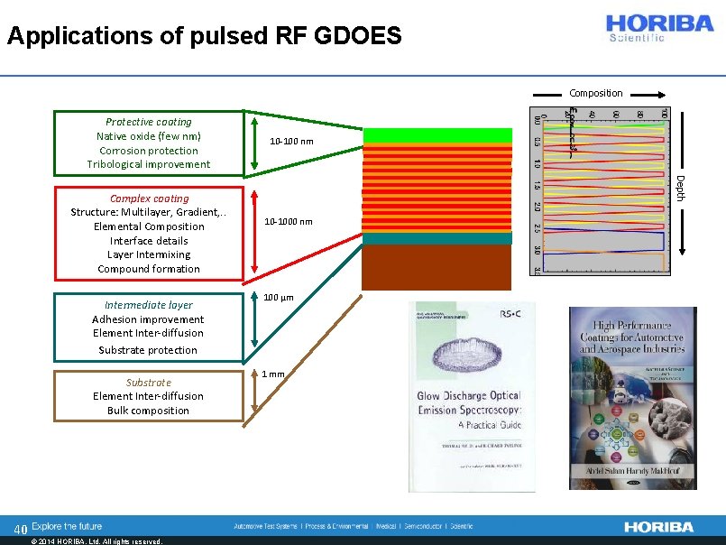
Applications of pulsed RF GDOES Composition Protective coating Native oxide (few nm) Corrosion protection Tribological improvement Intermediate layer Adhesion improvement Element Inter-diffusion Substrate protection Substrate Element Inter-diffusion Bulk composition 40 © 2014 HORIBA, Ltd. All rights reserved. Depth Complex coating Structure: Multilayer, Gradient, . . Elemental Composition Interface details Layer Intermixing Compound formation 10 -100 nm 10 -1000 nm 100 µm 1 mm

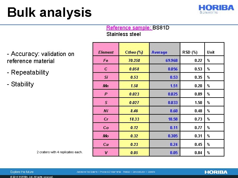
Bulk analysis Reference sample: BS 81 D Stainless steel - Accuracy: validation on Element Ctheo (%) reference material Fe 70. 258 69. 968 0. 22 % - Repeatability C 0. 058 0. 056 0. 53 % Si 0. 53 0. 35 % Mn 1. 58 1. 51 0. 20 % P 0. 023 0. 025 0. 89 % S 0. 027 0. 033 1. 50 % Ni 8. 46 8. 60 0. 48 % Cr 18. 33 18. 58 0. 73 % Co 0. 12 0. 11 0. 77 % Mo 0. 32 0. 305 0. 31 % Cu 0. 23 0. 24 0. 45 % V 0. 05 0. 84 % - Stability 2 craters with 4 replicates each. © 2014 HORIBA, Ltd. All rights reserved. Average RSD (%) Unit

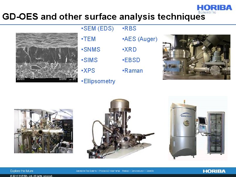
GD-OES and other surface analysis techniques • SEM (EDS) • RBS • TEM • AES (Auger) • SNMS • XRD • SIMS • EBSD • XPS • Raman • Ellipsometry © 2014 HORIBA, Ltd. All rights reserved.

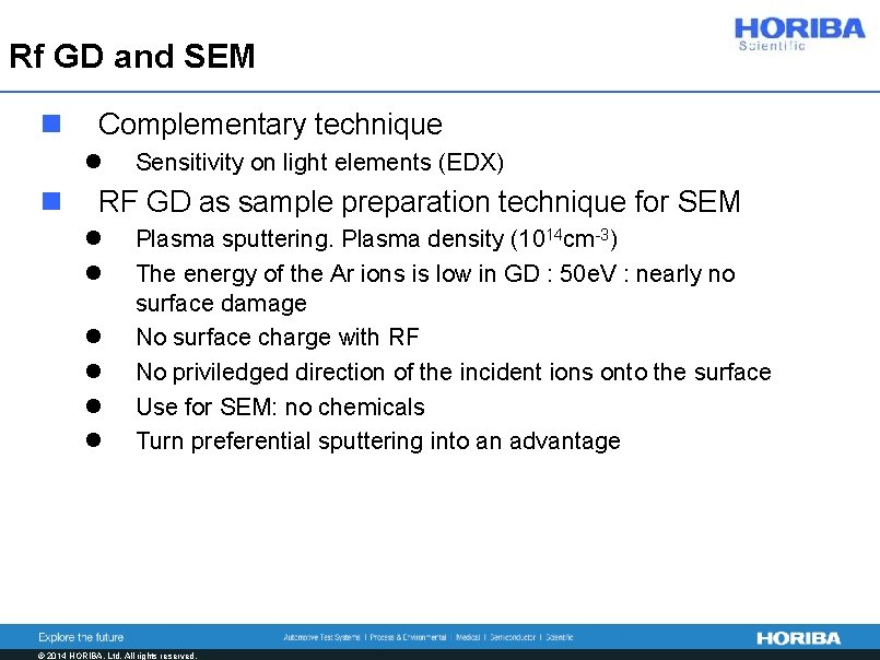
Rf GD and SEM n Complementary technique l n Sensitivity on light elements (EDX) RF GD as sample preparation technique for SEM l l l Plasma sputtering. Plasma density (1014 cm-3) The energy of the Ar ions is low in GD : 50 e. V : nearly no surface damage No surface charge with RF No priviledged direction of the incident ions onto the surface Use for SEM: no chemicals Turn preferential sputtering into an advantage © 2014 HORIBA, Ltd. All rights reserved.

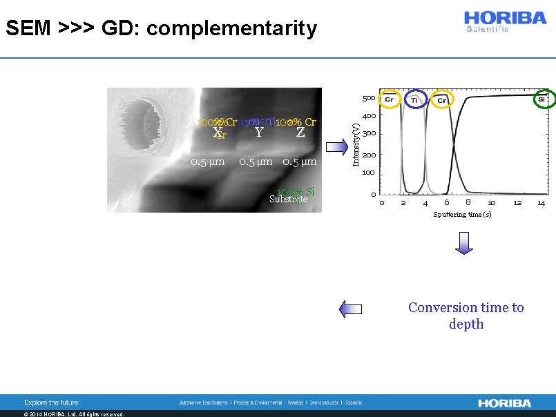
SEM >>> GD: complementarity 500 0. 5 µm 100% Si Substrate Si 400 Intensity (V) x%Cr 100% y% Ti z% Cr 100% Ti 100% X Y Z Cr 300 200 100 0 0 2 4 6 8 10 12 Concentration (%) Sputtering time (s) Conversion time to depth Depth (µm) © 2014 HORIBA, Ltd. All rights reserved. 14

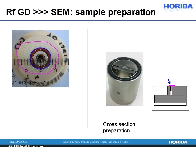
Rf GD >>> SEM: sample preparation Cross section preparation © 2014 HORIBA, Ltd. All rights reserved.

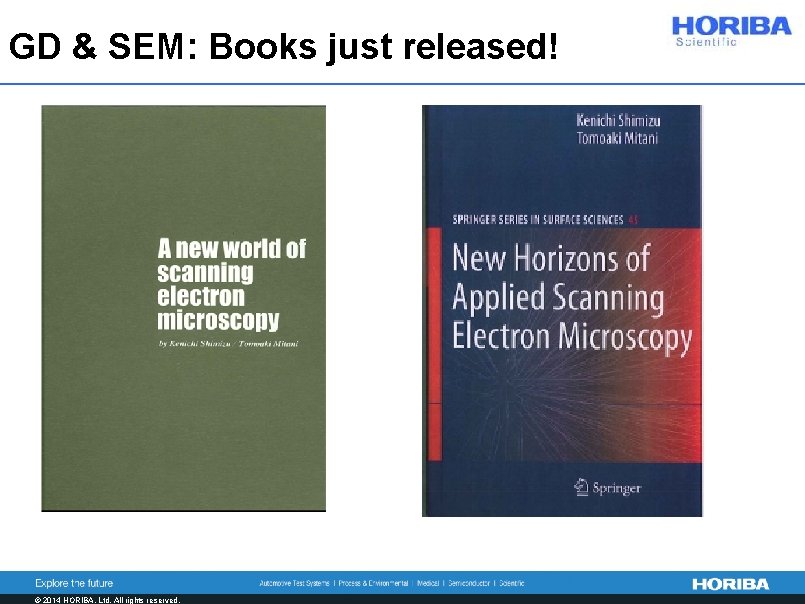
GD & SEM: Books just released! © 2014 HORIBA, Ltd. All rights reserved.

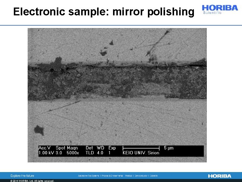
Electronic sample: mirror polishing © 2014 HORIBA, Ltd. All rights reserved.

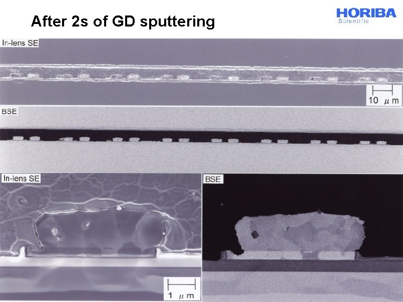
After 2 s of GD sputtering © 2014 HORIBA, Ltd. All rights reserved.

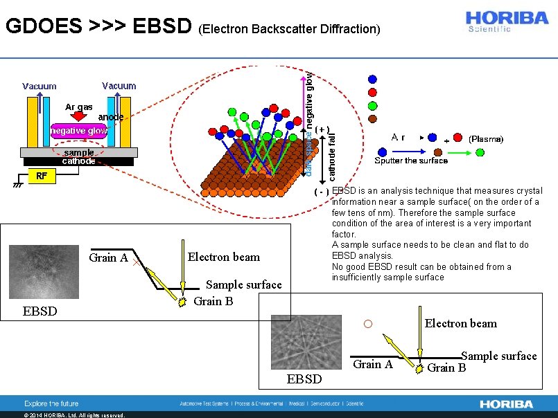
GDOES >>> EBSD (Electron Backscatter Diffraction) Grain A EBSD × EBSD is an analysis technique that measures crystal information near a sample surface( on the order of a few tens of nm). Therefore the sample surface condition of the area of interest is a very important factor. A sample surface needs to be clean and flat to do EBSD analysis. No good EBSD result can be obtained from a insufficiently sample surface Electron beam Sample surface Grain B ○ EBSD © 2014 HORIBA, Ltd. All rights reserved. Grain A Electron beam Sample surface Grain B

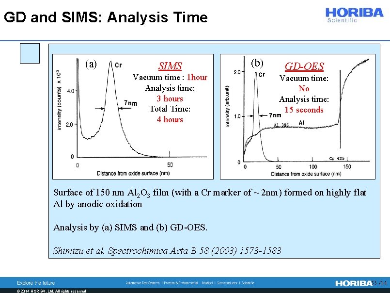
GD and SIMS: Analysis Time (a) SIMS Vacuum time : 1 hour Analysis time: 3 hours Total Time: 4 hours (b) GD-OES Vacuum time: No Analysis time: 15 seconds Surface of 150 nm Al 2 O 3 film (with a Cr marker of ~ 2 nm) formed on highly flat Al by anodic oxidation Analysis by (a) SIMS and (b) GD-OES. Shimizu et al. Spectrochimica Acta B 58 (2003) 1573 -1583 55 /14 © 2014 HORIBA, Ltd. All rights reserved.

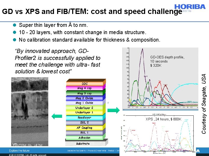
GD vs XPS and FIB/TEM: cost and speed challenge l Super thin layer from Å to nm. l 10 - 20 layers, with constant change in media structure. l No calibration standard available for thickness & composition. GD-OES depth profile, 10 seconds $ 320 K XPS , 24 hours, $ 800 K FIB/TEM, 8 h, >$2 M © 2014 HORIBA, Ltd. All rights reserved. Courtesy of Seagate, USA “By innovated approach, GDProfiler 2 is successfully applied to meet the challenge with ultra- fast solution & lowest cost”

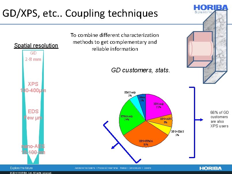
GD/XPS, etc. . Coupling techniques Spatial resolution GD 2 -8 mm To combine different characterization methods to get complementary and reliable information GD customers, stats. XPS 100 -400µm SIMS only 5% None 5% XPS only 21% EDS Few µm EPMAonly 24% XPS+AES 8% XPS+SIMS 5% nano-AES 10 -100 nm © 2014 HORIBA, Ltd. All rights reserved. XPS+EPMA 32% 66% of GD customers are also XPS users

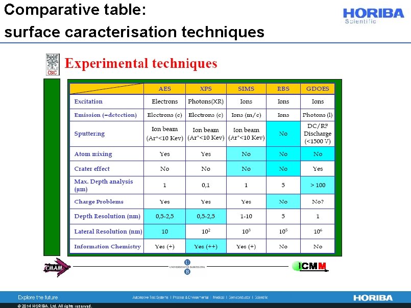
Comparative table: surface caracterisation techniques © 2014 HORIBA, Ltd. All rights reserved.

Linked. In : Join the GD group Infos on published papers, conferences attended, samples of interest etc. Open access: Ideas/contributions welcome © 2014 HORIBA, Ltd. All rights reserved.

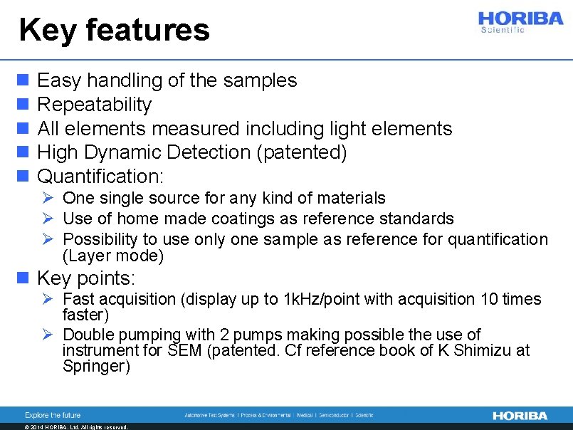
Key features n n n Easy handling of the samples Repeatability All elements measured including light elements High Dynamic Detection (patented) Quantification: Ø One single source for any kind of materials Ø Use of home made coatings as reference standards Ø Possibility to use only one sample as reference for quantification (Layer mode) n Key points: Ø Fast acquisition (display up to 1 k. Hz/point with acquisition 10 times faster) Ø Double pumping with 2 pumps making possible the use of instrument for SEM (patented. Cf reference book of K Shimizu at Springer) © 2014 HORIBA, Ltd. All rights reserved.