ESR 2 HighZ sensor materials on Medipix 3
![FLUORESCENCE IN HIGH-Z MATERIALS Mean free path of fluorescence photon [mm] Fluorescence yield [%] FLUORESCENCE IN HIGH-Z MATERIALS Mean free path of fluorescence photon [mm] Fluorescence yield [%]](https://slidetodoc.com/presentation_image_h/059c306ee1cdca9819f6e125f3087b13/image-8.jpg)
- Slides: 35

ESR 2 High-Z sensor materials on Medipix 3 RX Erik Fröjdh 1, 2, Rafael Ballabriga 2, Michael Campbell 2 1. 2. Mid Sweden University CERN ARDENT WORKSHOP 2014 - SCHWARZENBRUCK

OUTLINE • Summary of research activities • Comparison between Cd. Te, CZT and Silicon bump bonded to Medipix 3 RX – – – – Measurement setup Calibration Energy resolution Flat field at 25 ke. V Single pixel energy resolution First look at MTF with CZT assemblies Conclusions Future work

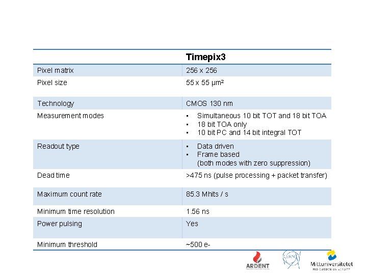
Timepix 3 Pixel matrix 256 Pixel size 55 x 55 μm 2 Technology CMOS 130 nm Measurement modes • • • Simultaneous 10 bit TOT and 18 bit TOA only 10 bit PC and 14 bit integral TOT Readout type • • Data driven Frame based (both modes with zero suppression) Dead time >475 ns (pulse processing + packet transfer) Maximum count rate 85. 3 Mhits / s Minimum time resolution 1. 56 ns Power pulsing Yes Minimum threshold ~500 e-

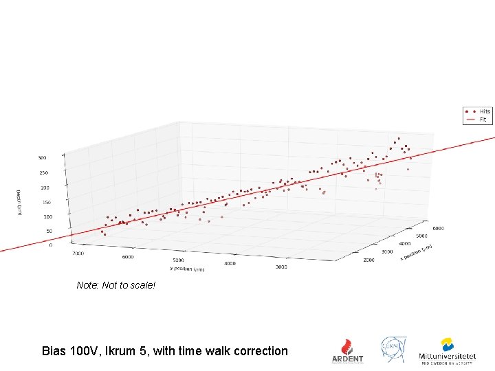
Note: Not to scale! Bias 100 V, Ikrum 5, with time walk correction

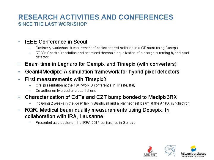
RESEARCH ACTIVITIES AND CONFERENCES SINCE THE LAST WORKSHOP • IEEE Conference in Seoul – – Dosimetry workshop: Measurement of backscattered radiation in a CT room using Dosepix RTSD: Spectral resolution and optimized threshold equalization of a charge summing hybrid pixel detector • Beam time in Legnaro for Gempix and Timepix (with converters) • Geant 4 Medipix: A simulation framework for hybrid pixel detectors • First measurements with Timepix 3 – – Oral presentation at the 16 th i. Wo. RID conference in Trieste, Italy Co author on two poster presentations • Characterization of Cd. Te and CZT bump bonded to Medipix 3 RX – Including 2 weeks in the X-ray lab in Sundsvall and a planned test beam at the ANKA synchrotron • RQR, Medical beam quality measurements using Dosepix. In collaboration with IRA, Lausanne – Presented as a poster on the IRPA 2014 conference in Geneva

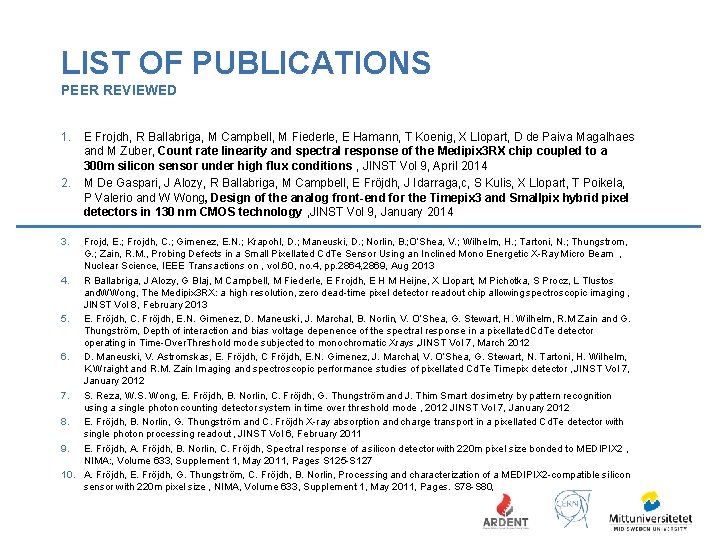
LIST OF PUBLICATIONS PEER REVIEWED 1. E Frojdh, R Ballabriga, M Campbell, M Fiederle, E Hamann, T Koenig, X Llopart, D de Paiva Magalhaes and M Zuber, Count rate linearity and spectral response of the Medipix 3 RX chip coupled to a 300 m silicon sensor under high flux conditions , JINST Vol 9, April 2014 2. M De Gaspari, J Alozy, R Ballabriga, M Campbell, E Fröjdh, J Idarraga, c, S Kulis, X Llopart, T Poikela, P Valerio and W Wong, Design of the analog front-end for the Timepix 3 and Smallpix hybrid pixel detectors in 130 nm CMOS technology , JINST Vol 9, January 2014 3. Frojd, E. ; Frojdh, C. ; Gimenez, E. N. ; Krapohl, D. ; Maneuski, D. ; Norlin, B. ; O’Shea, V. ; Wilhelm, H. ; Tartoni, N. ; Thungstrom, G. ; Zain, R. M. , Probing Defects in a Small Pixellated Cd. Te Sensor Using an Inclined Mono Energetic X-Ray Micro Beam , Nuclear Science, IEEE Transactions on , vol. 60, no. 4, pp. 2864, 2869, Aug. 2013 4. R Ballabriga, J Alozy, G Blaj, M Campbell, M Fiederle, E Frojdh, E H M Heijne, X Llopart, M Pichotka, S Procz, L Tlustos and. WWong, The Medipix 3 RX: a high resolution, zero dead-time pixel detector readout chip allowing spectroscopic imaging , JINST Vol 8, February 2013 5. E. Fröjdh, C. Fröjdh, E. N. Gimenez, D. Maneuski, J. Marchal, B. Norlin, V. O’Shea, G. Stewart, H. Wilhelm, R. M Zain and G. Thungström, Depth of interaction and bias voltage depenence of the spectral response in a pixellated Cd. Te detector operating in Time-Over. Threshold mode subjected to monochromatic Xrays , JINST Vol 7, March 2012 6. D. Maneuski, V. Astromskas, E. Fröjdh, C Fröjdh, E. N. Gimenez, J. Marchal, V. O’Shea, G. Stewart, N. Tartoni, H. Wilhelm, K. Wraight and R. M. Zain Imaging and spectroscopic performance studies of pixellated Cd. Te Timepix detector , JINST Vol 7, January 2012 7. S. Reza, W. S. Wong, E. Fröjdh, B. Norlin, C. Fröjdh, G. Thungström and J. Thim Smart dosimetry by pattern recognition using a single photon counting detector system in time over threshold mode , 2012 JINST Vol 7, January 2012 8. E. Fröjdh, B. Norlin, G. Thungström and C. Fröjdh X-ray absorption and charge transport in a pixellated Cd. Te detector with single photon processing readout , JINST Vol 6, February 2011 9. E. Fröjdh, A. Fröjdh, B. Norlin, C. Fröjdh, Spectral response of a silicon detector with 220 m pixel size bonded to MEDIPIX 2 , NIMA: , Volume 633, Supplement 1, May 2011, Pages S 125 -S 127 10. A. Fröjdh, E. Fröjdh, G. Thungström, C. Fröjdh, B. Norlin, Processing and characterization of a MEDIPIX 2 -compatible silicon sensor with 220 m pixel size , NIMA, Volume 633, Supplement 1, May 2011, Pages. S 78 -S 80,

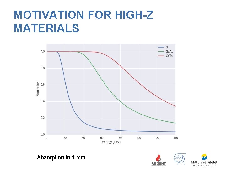
MOTIVATION FOR HIGH-Z MATERIALS Absorption in 1 mm
![FLUORESCENCE IN HIGHZ MATERIALS Mean free path of fluorescence photon mm Fluorescence yield FLUORESCENCE IN HIGH-Z MATERIALS Mean free path of fluorescence photon [mm] Fluorescence yield [%]](https://slidetodoc.com/presentation_image_h/059c306ee1cdca9819f6e125f3087b13/image-8.jpg)
FLUORESCENCE IN HIGH-Z MATERIALS Mean free path of fluorescence photon [mm] Fluorescence yield [%] Energy fluorescence photons [ke. V] Z The mean free path of the fluorescence photons is in the same order of magnitude as the pixel pitch The fluorescence yield increases with the atomic number Table: L. Tlustos, Ph. D thesis

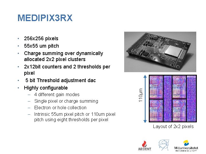
• 256 x 256 pixels • 55 x 55 um pitch • Charge summing over dynamically allocated 2 x 2 pixel clusters • 2 x 12 bit counters and 2 thresholds per pixel • 5 bit Threshold adjustment dac • Highly configurable – – 4 different gain modes Single pixel or charge summing Electron or hole collection Intrinsic 55 um pixel pitch or 110 um pixel pitch using eight thresholds per pixel 110μm MEDIPIX 3 RX Layout of 2 x 2 pixels

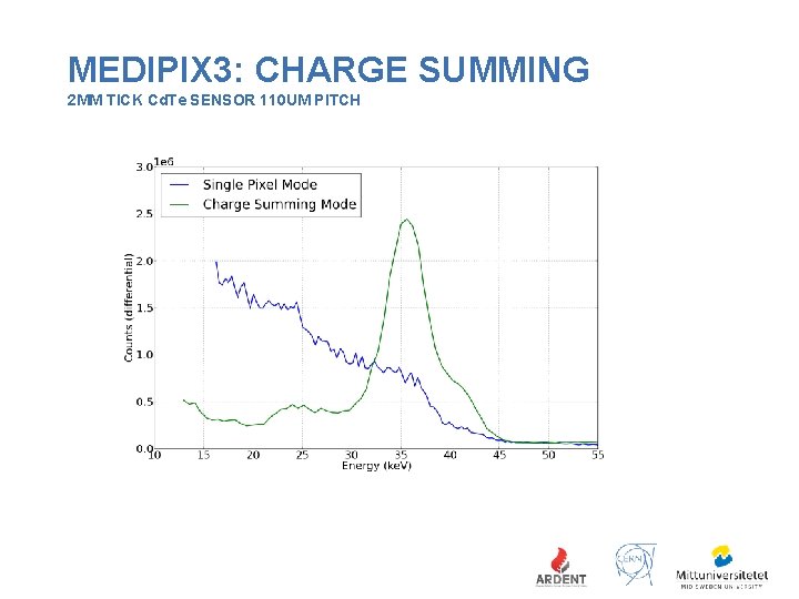
MEDIPIX 3: CHARGE SUMMING 2 MM TICK Cd. Te SENSOR 110 UM PITCH

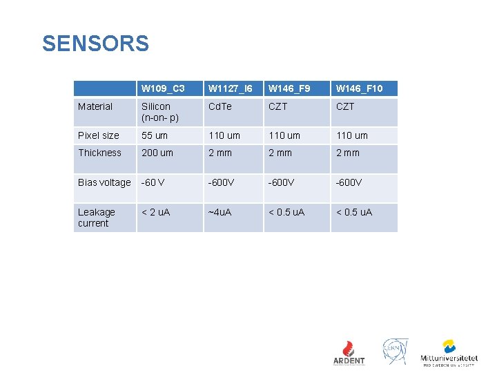
SENSORS W 109_C 3 W 1127_I 6 W 146_F 9 W 146_F 10 Material Silicon (n-on- p) Cd. Te CZT Pixel size 55 um 110 um Thickness 200 um 2 mm Bias voltage -60 V -600 V Leakage current < 2 u. A ~4 u. A < 0. 5 u. A

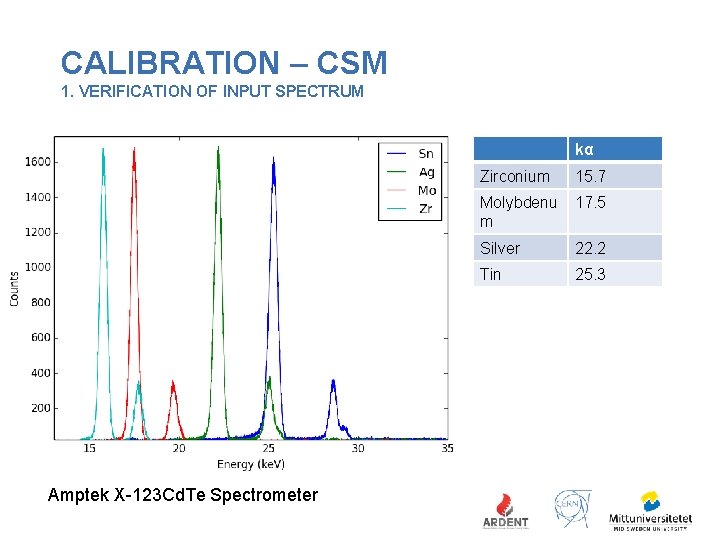
CALIBRATION – CSM 1. VERIFICATION OF INPUT SPECTRUM kα Amptek X-123 Cd. Te Spectrometer Zirconium 15. 7 Molybdenu m 17. 5 Silver 22. 2 Tin 25. 3

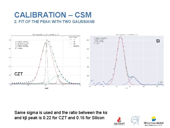
CALIBRATION – CSM 2. FIT OF THE PEAK WITH TWO GAUSSIANS Si CZT ke. V Same sigma is used and the ratio between the kα and kβ peak is 0. 22 for CZT and 0. 16 for Silicon

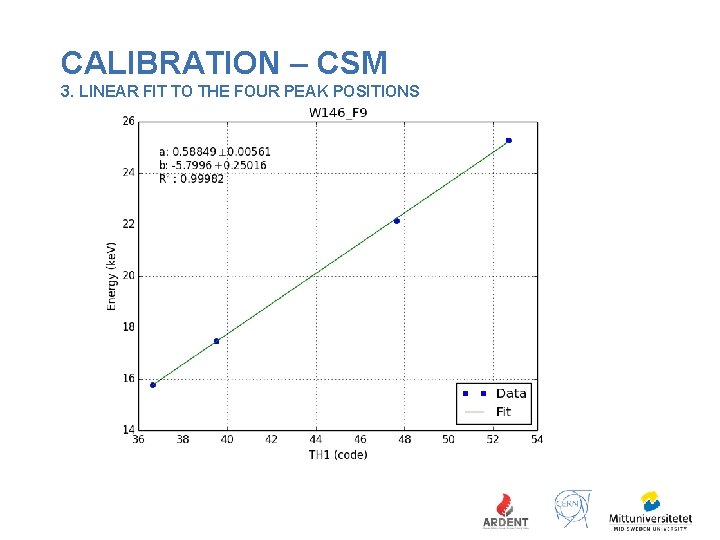
CALIBRATION – CSM 3. LINEAR FIT TO THE FOUR PEAK POSITIONS

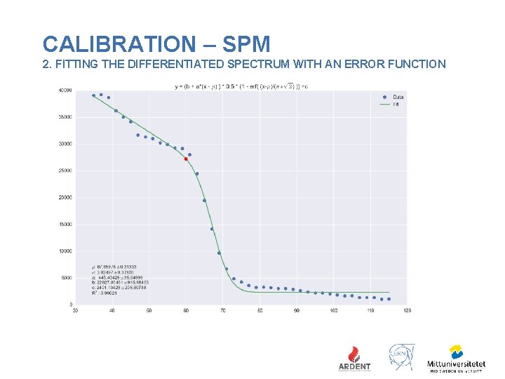
CALIBRATION – SPM 2. FITTING THE DIFFERENTIATED SPECTRUM WITH AN ERROR FUNCTION

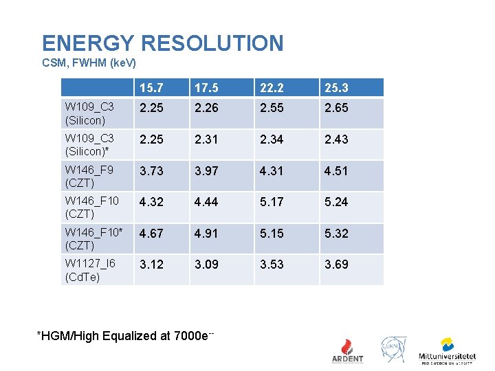
ENERGY RESOLUTION CSM, FWHM (ke. V) 15. 7 17. 5 22. 2 25. 3 W 109_C 3 (Silicon) 2. 25 2. 26 2. 55 2. 65 W 109_C 3 (Silicon)* 2. 25 2. 31 2. 34 2. 43 W 146_F 9 (CZT) 3. 73 3. 97 4. 31 4. 51 W 146_F 10 (CZT) 4. 32 4. 44 5. 17 5. 24 W 146_F 10* (CZT) 4. 67 4. 91 5. 15 5. 32 W 1127_I 6 (Cd. Te) 3. 12 3. 09 3. 53 3. 69 *HGM/High Equalized at 7000 e--

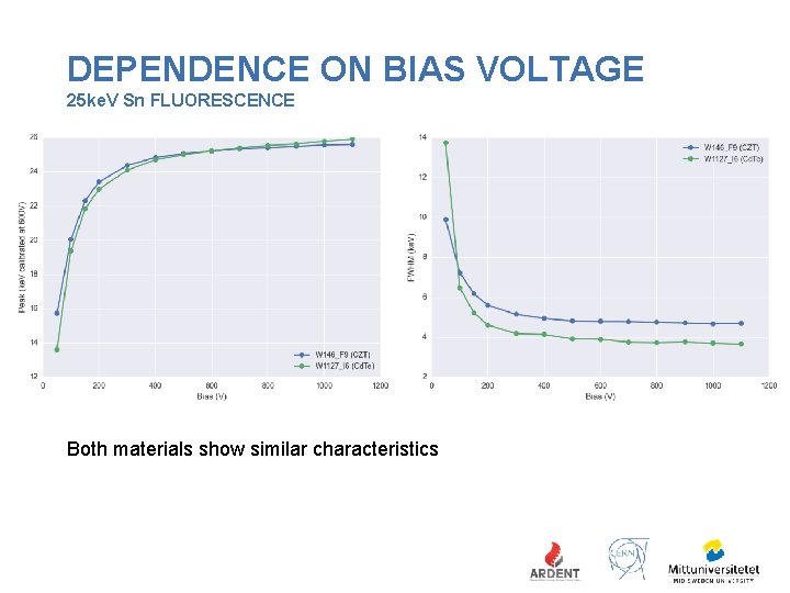
DEPENDENCE ON BIAS VOLTAGE 25 ke. V Sn FLUORESCENCE Both materials show similar characteristics

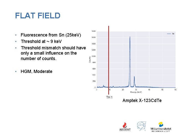
FLAT FIELD • Fluorescence from Sn (25 ke. V) • Threshold at ~ 9 ke. V • Threshold mismatch should have only a small influence on the number of counts. • HGM, Moderate TH 1 Amptek X-123 Cd. Te

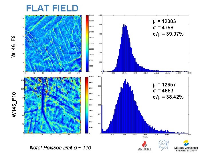
FLAT FIELD W 146_F 9 μ = 12003 σ = 4798 σ/μ = 39. 97% W 146_F 10 μ = 12657 σ = 4863 σ/μ = 38. 42% Note! Poisson limit σ ~ 110

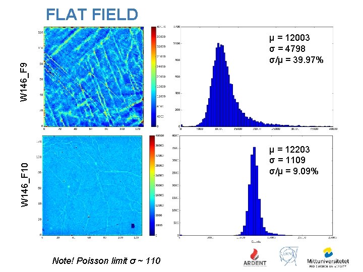
FLAT FIELD W 146_F 9 μ = 12003 σ = 4798 σ/μ = 39. 97% W 146_F 10 μ = 12203 σ = 1109 σ/μ = 9. 09% Note! Poisson limit σ ~ 110

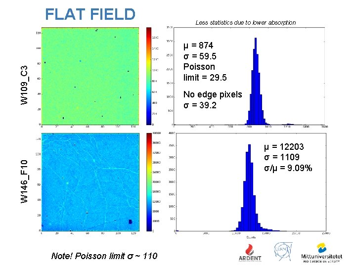
FLAT FIELD Less statistics due to lower absorption W 109_C 3 μ = 874 σ = 59. 5 Poisson limit = 29. 5 No edge pixels σ = 39. 2 W 146_F 10 μ = 12203 σ = 1109 σ/μ = 9. 09% Note! Poisson limit σ ~ 110

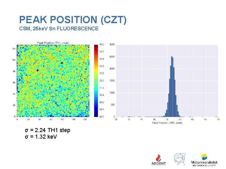
PEAK POSITION (CZT) CSM, 25 ke. V Sn FLUORESCENCE σ = 2. 24 TH 1 step σ = 1. 32 ke. V

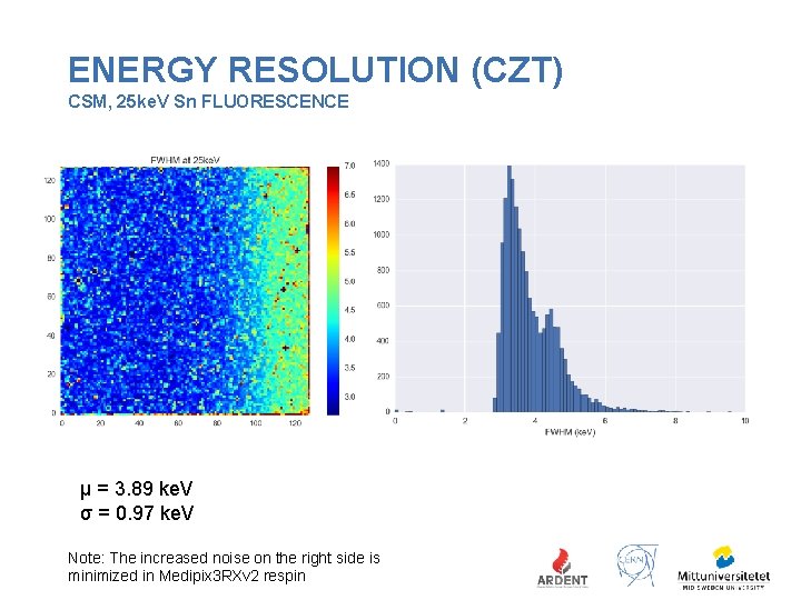
ENERGY RESOLUTION (CZT) CSM, 25 ke. V Sn FLUORESCENCE μ = 3. 89 ke. V σ = 0. 97 ke. V Note: The increased noise on the right side is minimized in Medipix 3 RXv 2 respin

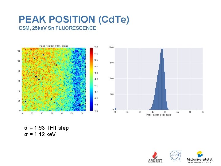
PEAK POSITION (Cd. Te) CSM, 25 ke. V Sn FLUORESCENCE σ = 1. 93 TH 1 step σ = 1. 12 ke. V

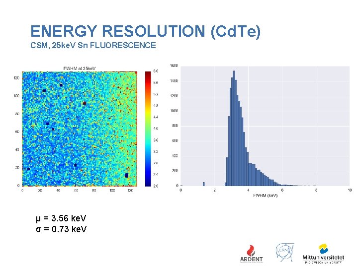
ENERGY RESOLUTION (Cd. Te) CSM, 25 ke. V Sn FLUORESCENCE μ = 3. 56 ke. V σ = 0. 73 ke. V

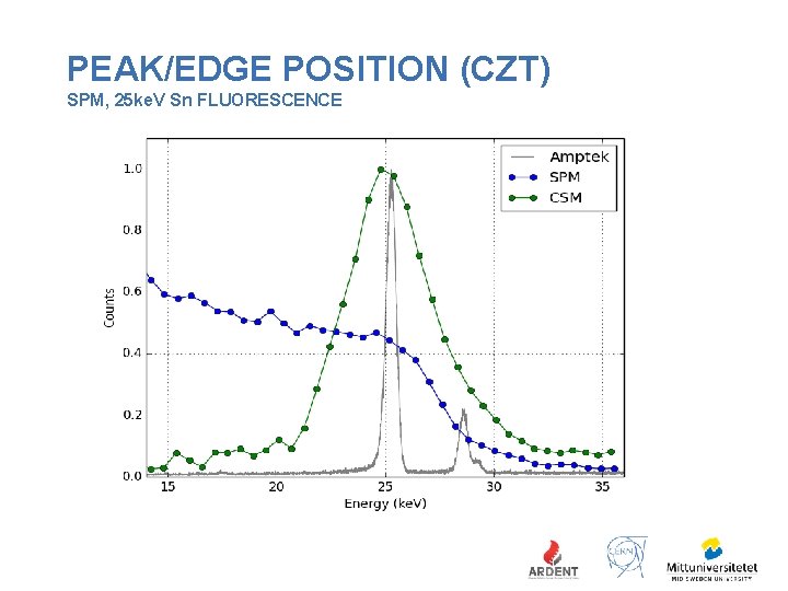
PEAK/EDGE POSITION (CZT) SPM, 25 ke. V Sn FLUORESCENCE

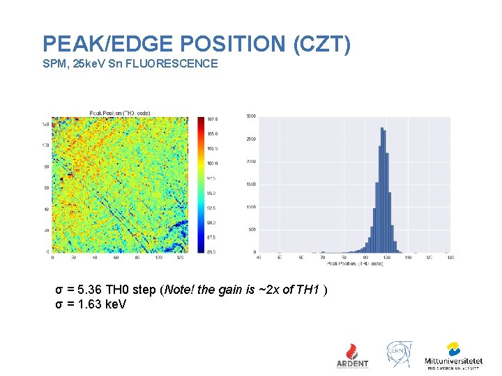
PEAK/EDGE POSITION (CZT) SPM, 25 ke. V Sn FLUORESCENCE σ = 5. 36 TH 0 step (Note! the gain is ~2 x of TH 1 ) σ = 1. 63 ke. V

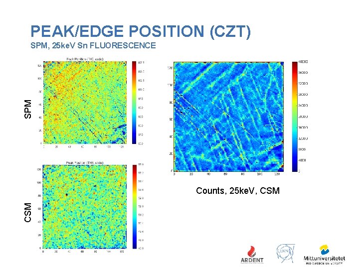
PEAK/EDGE POSITION (CZT) SPM, 25 ke. V Sn FLUORESCENCE CSM Counts, 25 ke. V, CSM

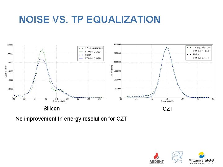
NOISE VS. TP EQUALIZATION Silicon No improvement In energy resolution for CZT

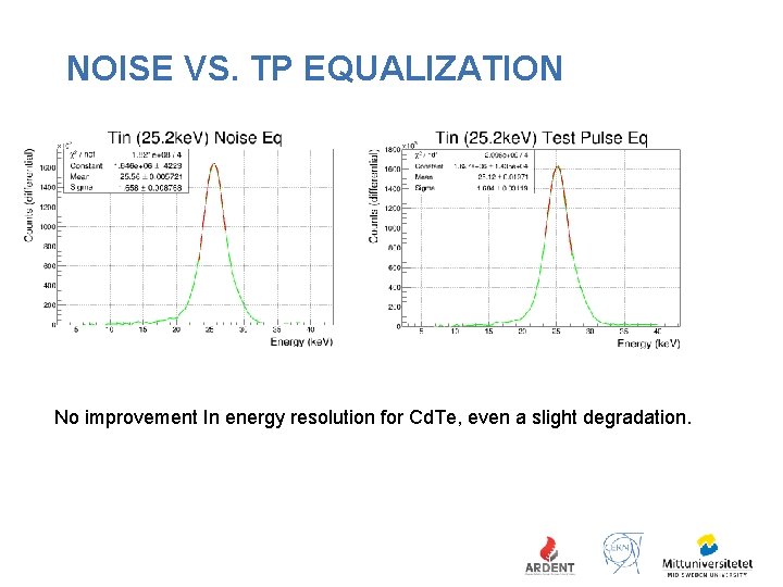
NOISE VS. TP EQUALIZATION No improvement In energy resolution for Cd. Te, even a slight degradation.

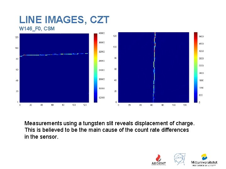
LINE IMAGES, CZT W 146_F 0, CSM Measurements using a tungsten slit reveals displacement of charge. This is believed to be the main cause of the count rate differences in the sensor.

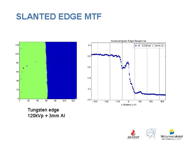
SLANTED EDGE MTF Tungsten edge 120 k. Vp + 3 mm Al

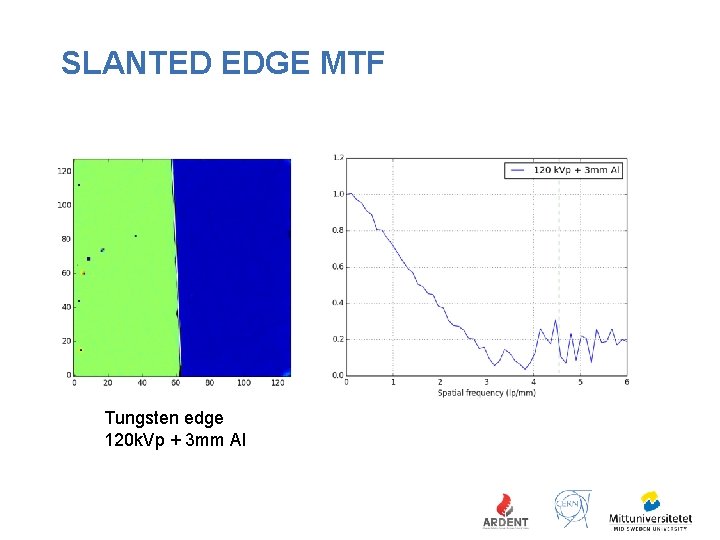
SLANTED EDGE MTF Tungsten edge 120 k. Vp + 3 mm Al

CONCLUSIONS • Both Cd. Te and CZT displays good energy resolution across the sensor • The lack of improvement in energy resolution using a test pulse calibration suggest gain differences induced by the sensor for both Cd. Te and CZT • Large count rate differences are observed in the CZT sensors, probably caused by charge displacement due to an inhomogeneous electrical field • Imagining performance is greatly affected by this charge displacement

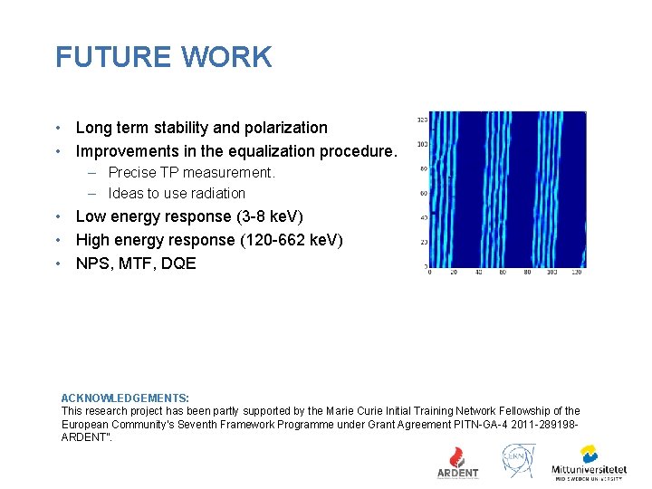
FUTURE WORK • Long term stability and polarization • Improvements in the equalization procedure. – Precise TP measurement. – Ideas to use radiation • Low energy response (3 -8 ke. V) • High energy response (120 -662 ke. V) • NPS, MTF, DQE ACKNOWLEDGEMENTS: This research project has been partly supported by the Marie Curie Initial Training Network Fellowship of the European Community’s Seventh Framework Programme under Grant Agreement PITN-GA-4 2011 -289198 ARDENT”.