EGN 3373 Introduction to Electrical Systems I A





- Slides: 58

EGN 3373 Introduction to Electrical Systems I A Systems Approach to Electrical Engineering Graphics Adapted from “Physical, Earth, and Space Science”, Tom Hsu, cpo. Science.

Chapter 8 - Diodes Objectives: 1. 2. 3. 4. Understand diode operation and select diodes for various applications Use the ideal diode model to analyze nonlinear circuits Analyze and design simple voltage-regulator circuits Use the constant voltage model Application 1. Most common application is rectification (converts ac to dc) e. g. automotive alternator, voltage multipliers, power conversion 2. Voltage protection (voltage spikes) e. g. stepper motor 3. Combination circuits, e. g. logic gates, temperature gauge 4. More diodes - Used to regulate voltage (Zener diodes), electronically tune radio and TV receivers (varactor diodes), generate radio frequency oscillations (tunnel diodes), or produce light (light emitting diodes - LED)

Solid-State Electronics – electrical devices and circuits containing active elements capable of controlling the flow of current If current is thought of as the flow of electrons, the name “electronics” makes perfect sense. 3

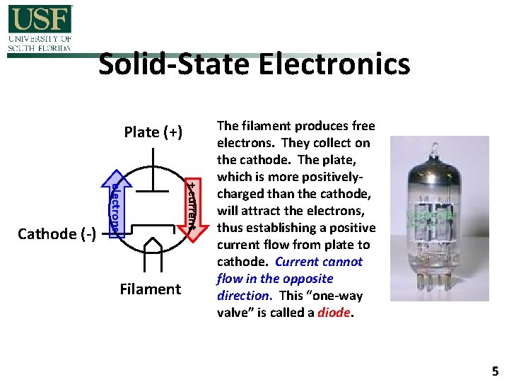
Solid-State Electronics For many years, the active components in electronic circuits were thermionic devices called vacuum tubes. Vacuum tubes used electric current to heat a metal filament, which gave off free electrons. The negatively-charged electrons traveled through a vacuum to a positively-charged plate. 4

Solid-State Electronics Plate (+) Filament + current electrons Cathode (-) The filament produces free electrons. They collect on the cathode. The plate, which is more positivelycharged than the cathode, will attract the electrons, thus establishing a positive current flow from plate to cathode. Current cannot flow in the opposite direction. This “one-way valve” is called a diode. 5

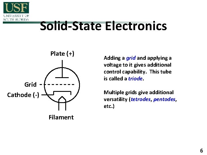
Solid-State Electronics Plate (+) Grid Cathode (-) Adding a grid and applying a voltage to it gives additional control capability. This tube is called a triode. Multiple grids give additional versatility (tetrodes, pentodes, etc. ) Filament 6

Solid-State Electronics Today, vacuum tubes are used only for niche applications (such as very high quality audio amplifiers) or where voltages and powers are very high (like radar). Most electronic applications are implemented using devices that operate in the solid state, not the gaseous state. 7

Solid-State Electronics Vacuum tubes work very well, but have some inherent issues: 1. They require LOTS of power to produce the heat needed to liberate free electrons. 2. They can be miniaturized to the size of a small light bulb, but modern devices require miniaturization several THOUSANDS of times smaller than that. 3. Because of the degradation of the filament, their useful life is shorter than we would like. 8

Solid-State Electronics Solid state devices address these issues. 1. Solid-state devices consume small amounts of power. 2. Solid-state devices can be minaturized to a very high degree – millions of devices per square centimeter. 3. Solid-state devices have long lifetimes – for some devices, many tens if not hundreds of years. 9

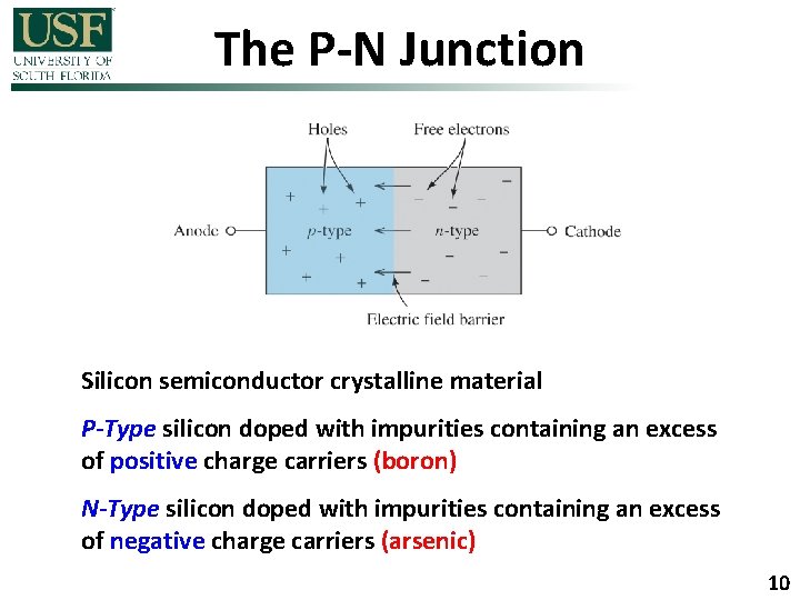
The P-N Junction Silicon semiconductor crystalline material P-Type silicon doped with impurities containing an excess of positive charge carriers (boron) N-Type silicon doped with impurities containing an excess of negative charge carriers (arsenic) 10

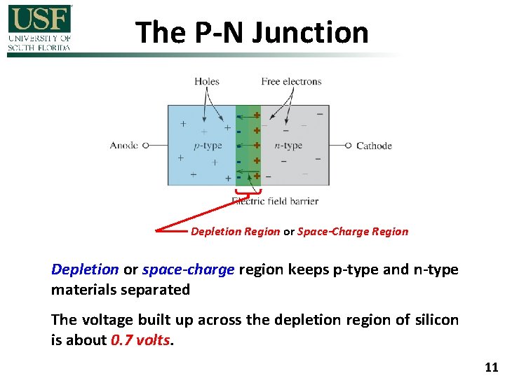
The P-N Junction - + + + Depletion Region or Space-Charge Region Depletion or space-charge region keeps p-type and n-type materials separated The voltage built up across the depletion region of silicon is about 0. 7 volts. 11

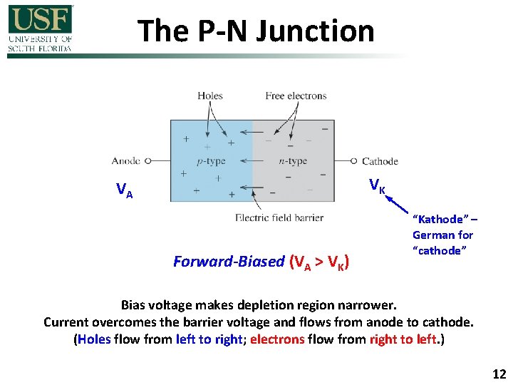
The P-N Junction VK VA Forward-Biased (VA > VK) “Kathode” – German for “cathode” Bias voltage makes depletion region narrower. Current overcomes the barrier voltage and flows from anode to cathode. (Holes flow from left to right; electrons flow from right to left. ) 12

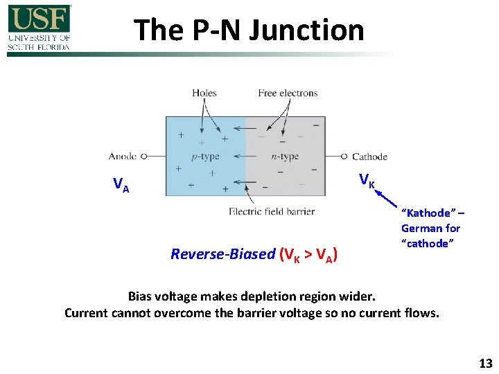
The P-N Junction VK VA Reverse-Biased (VK > VA) “Kathode” – German for “cathode” Bias voltage makes depletion region wider. Current cannot overcome the barrier voltage so no current flows. 13

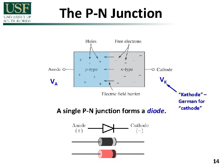
The P-N Junction VA VK A single P-N junction forms a diode. “Kathode” – German for “cathode” 14

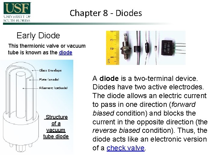
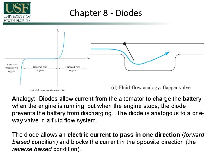
Chapter 8 - Diodes Early Diode This thermionic valve or vacuum tube is known as the diode Structure of a vacuum tube diode A diode is a two-terminal device. Diodes have two active electrodes. The diode allows an electric current to pass in one direction (forward biased condition) and blocks the current in the opposite direction (the reverse biased condition). Thus, the diode acts like an electronic version of a check valve.

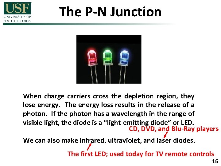
The P-N Junction When charge carriers cross the depletion region, they lose energy. The energy loss results in the release of a photon. If the photon has a wavelength in the range of visible light, the diode is a “light-emitting diode” or LED. CD, DVD, and Blu-Ray players We can also make infrared, ultraviolet, and laser diodes. The first LED; used today for TV remote controls 16

Chapter 8 - Diodes Analogy: Diodes allow current from the alternator to charge the battery when the engine is running, but when the engine stops, the diode prevents the battery from discharging. The diode is analogous to a oneway valve in a fluid flow system. The diode allows an electric current to pass in one direction (forward biased condition) and blocks the current in the opposite direction (the reverse biased condition).

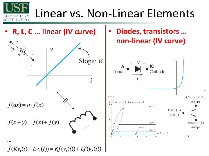
Linear vs. Non-Linear Elements • R, L, C … linear (IV curve) • Diodes, transistors … non-linear (IV curve)

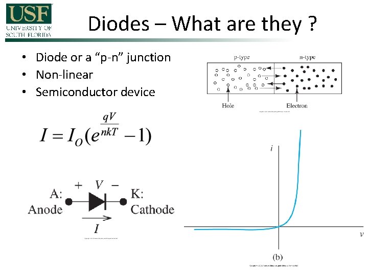
Diodes – What are they ? • Diode or a “p-n” junction • Non-linear • Semiconductor device

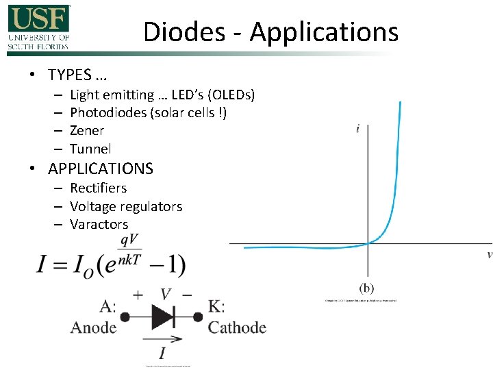
Diodes - Applications • TYPES … – – Light emitting … LED’s (OLEDs) Photodiodes (solar cells !) Zener Tunnel • APPLICATIONS – Rectifiers – Voltage regulators – Varactors

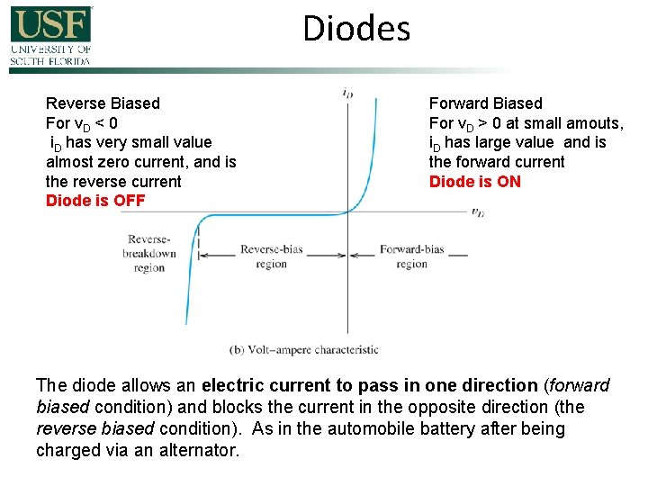
Diodes Reverse Biased For v. D < 0 i. D has very small value almost zero current, and is the reverse current Diode is OFF Forward Biased For v. D > 0 at small amouts, i. D has large value and is the forward current Diode is ON The diode allows an electric current to pass in one direction (forward biased condition) and blocks the current in the opposite direction (the reverse biased condition). As in the automobile battery after being charged via an alternator.

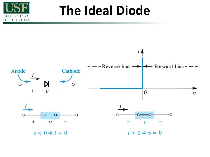
The Ideal Diode

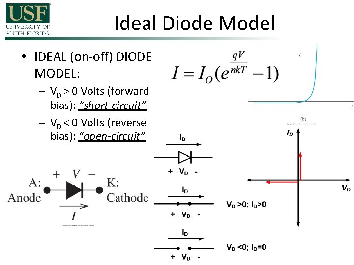
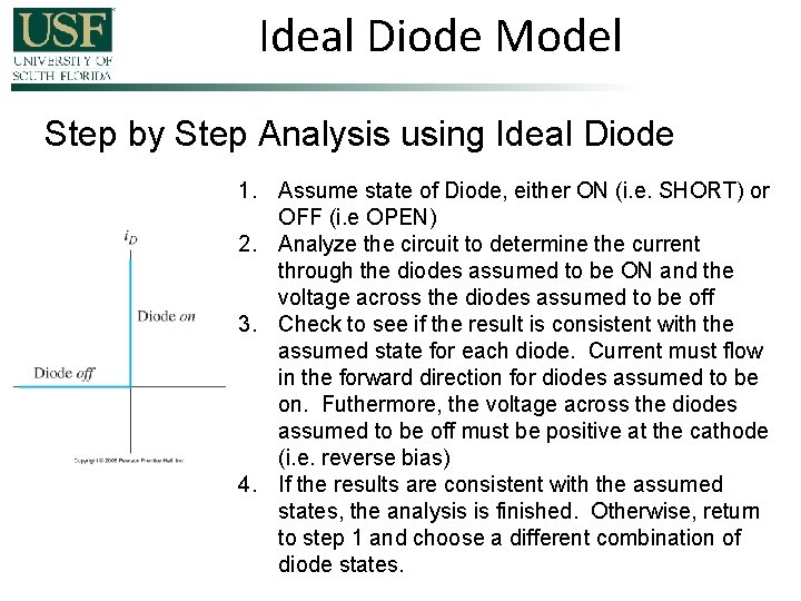
Ideal Diode Model • IDEAL (on-off) DIODE MODEL: – VD > 0 Volts (forward bias); “short-circuit” – VD < 0 Volts (reverse bias): “open-circuit”

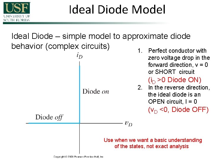
Ideal Diode Model Ideal Diode – simple model to approximate diode behavior (complex circuits) 1. Perfect conductor with zero voltage drop in the forward direction, v = 0 or SHORT circuit (i. D >0 Diode ON) 2. In the reverse direction, the ideal diode is an OPEN circuit, I = 0 (v. D <0, Diode OFF) Use when we want a basic understanding of the states, not exact analysis

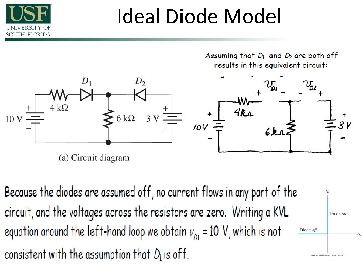
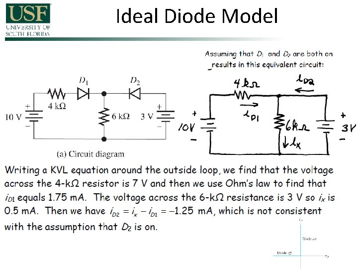
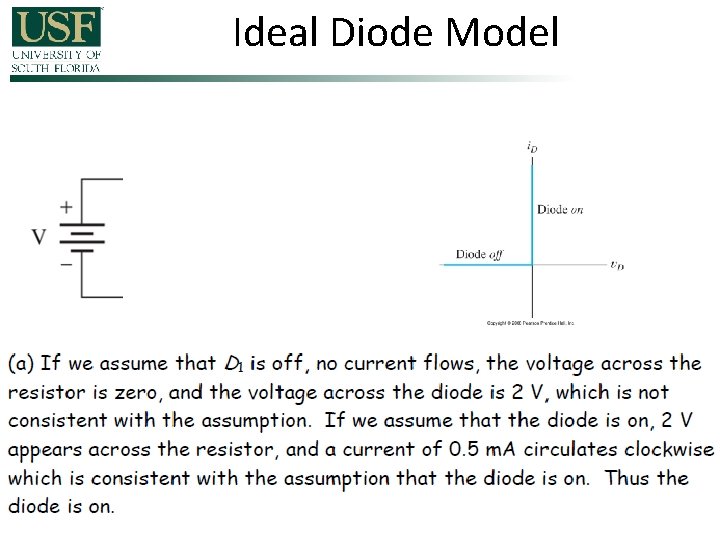
Ideal Diode Model Step by Step Analysis using Ideal Diode 1. Assume state of Diode, either ON (i. e. SHORT) or OFF (i. e OPEN) 2. Analyze the circuit to determine the current through the diodes assumed to be ON and the voltage across the diodes assumed to be off 3. Check to see if the result is consistent with the assumed state for each diode. Current must flow in the forward direction for diodes assumed to be on. Futhermore, the voltage across the diodes assumed to be off must be positive at the cathode (i. e. reverse bias) 4. If the results are consistent with the assumed states, the analysis is finished. Otherwise, return to step 1 and choose a different combination of diode states.

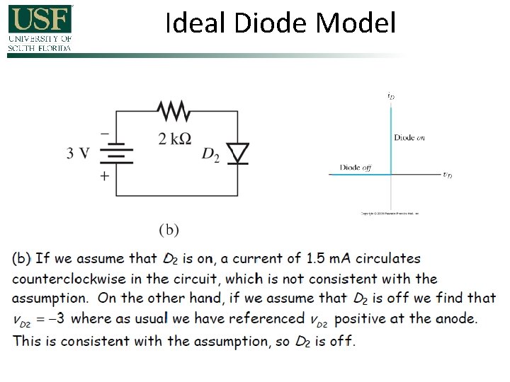
Ideal Diode Model

Ideal Diode Model

Ideal Diode Model

Ideal Diode Model

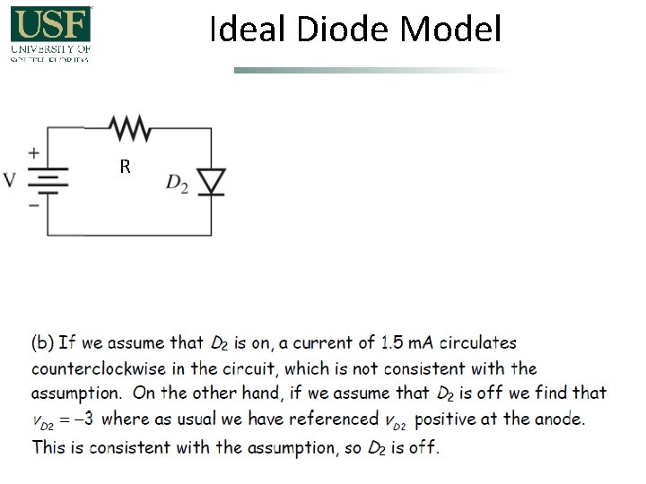
Ideal Diode Model R

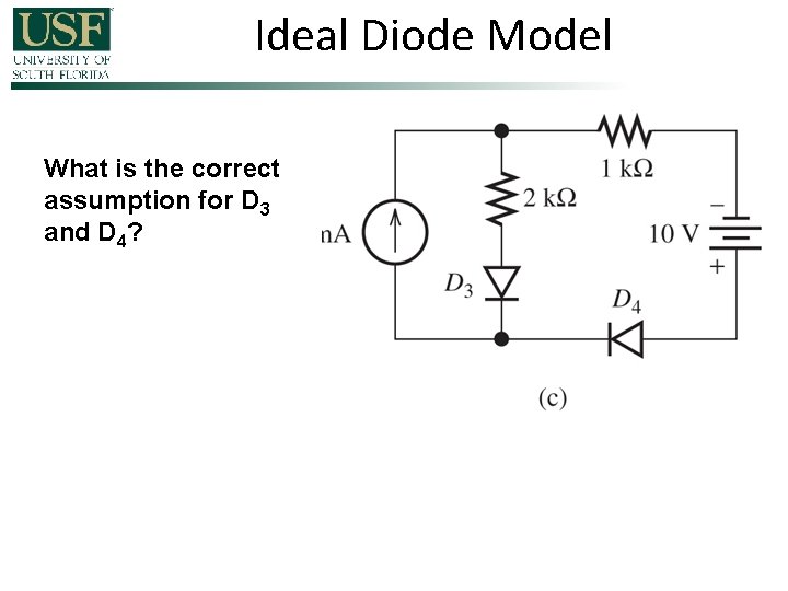
Ideal Diode Model What is the correct assumption for D 3 and D 4?

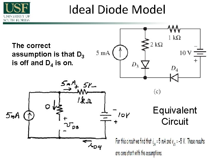
Ideal Diode Model The correct assumption is that D 3 is off and D 4 is on. Equivalent Circuit

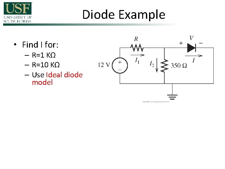
Diode Example • Find I for: – R=1 KΩ – R=10 KΩ – Use Ideal diode model

Diode Example • Find I for: – R=1 KΩ – R=10 KΩ – Use Ideal diode model

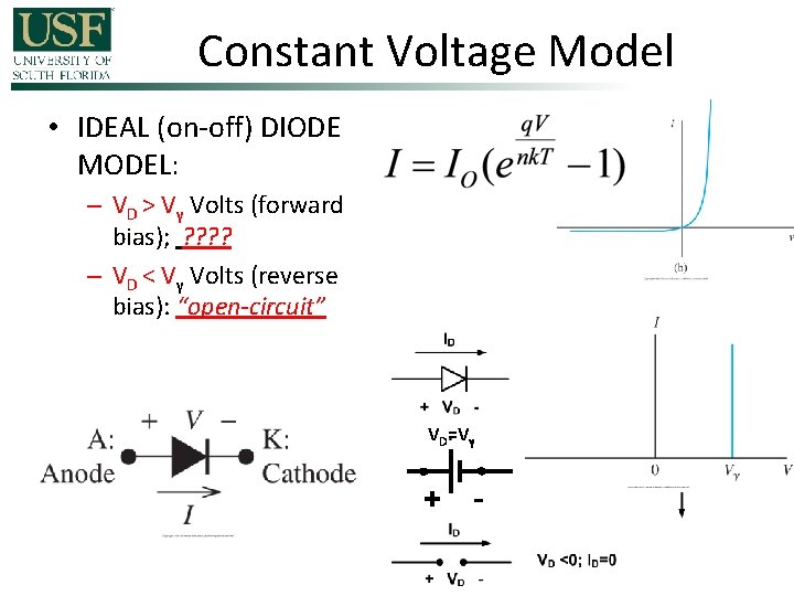
Constant Voltage Model • IDEAL (on-off) DIODE MODEL: – VD > Vγ Volts (forward bias); ? ? – VD < Vγ Volts (reverse bias): “open-circuit” VD=Vγ + -

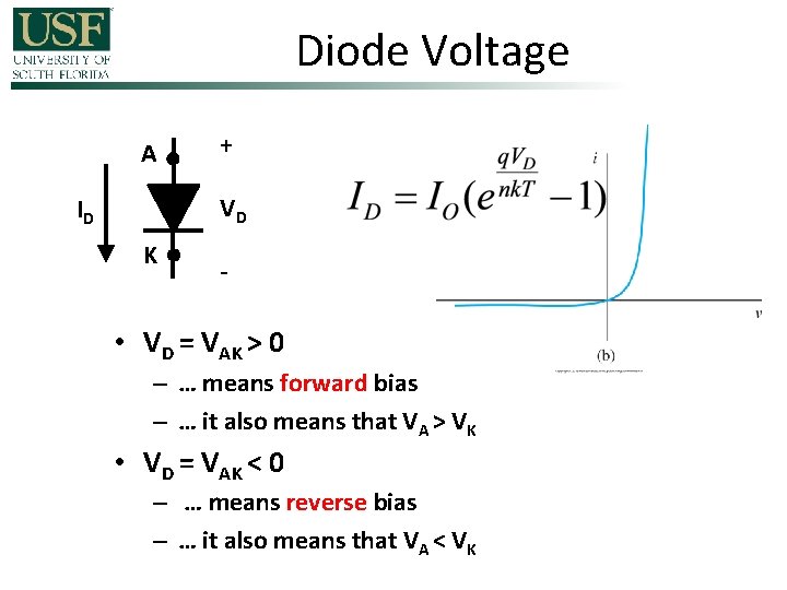
Diode Voltage A + VD ID K - • VD = VAK > 0 – … means forward bias – … it also means that VA > VK • VD = VAK < 0 – … means reverse bias – … it also means that VA < VK

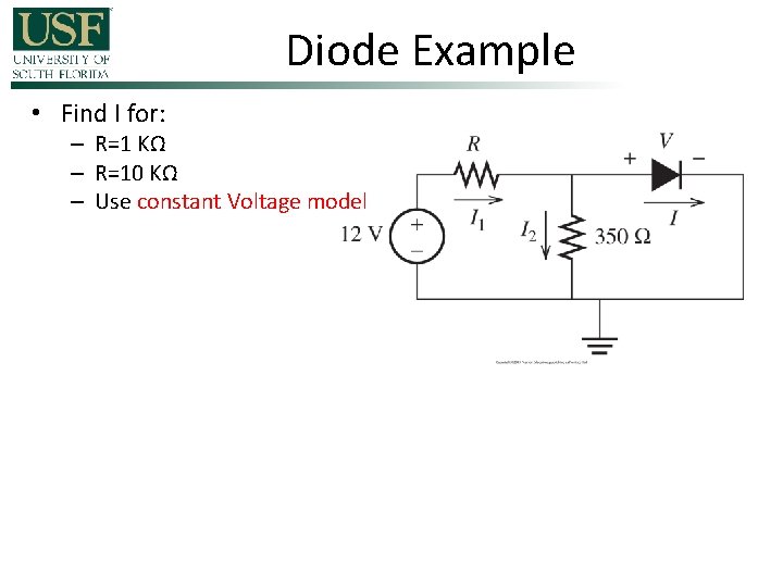
Diode Example • Find I for: – R=1 KΩ – R=10 KΩ – Use constant Voltage model

Diode Example • Find I for: – R=1 KΩ – R=10 KΩ – Use constant Voltage model

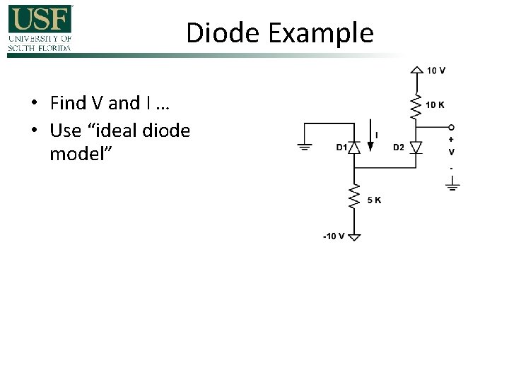
Diode Example • Find V and I … • Use “ideal diode model”

Diode Example • Find V and I … • Use “ideal diode model”

Diode Example • Find V and I … • Use “ideal diode model”

Diode Example

Diode Example

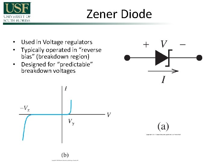
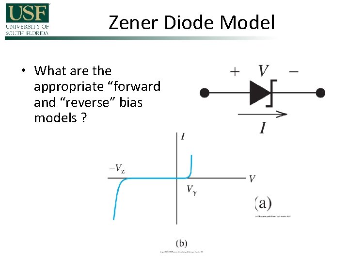
Zener Diode • Used in Voltage regulators • Typically operated in “reverse bias” (breakdown region) • Designed for “predictable” breakdown voltages

Zener Diode Model • What are the appropriate “forward and “reverse” bias models ?

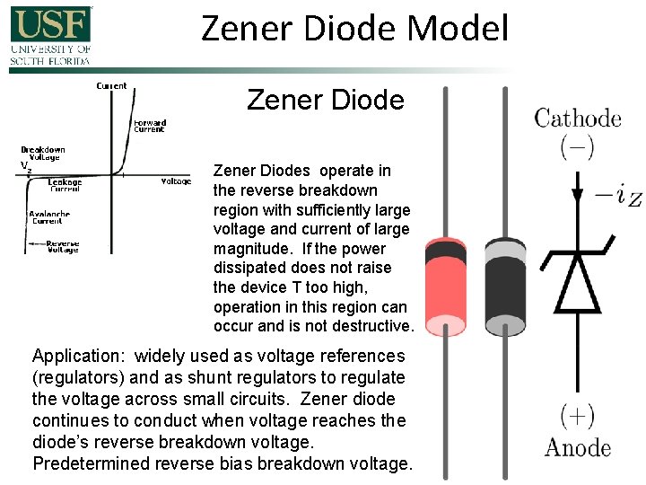
Zener Diode Model Zener Diodes operate in the reverse breakdown region with sufficiently large voltage and current of large magnitude. If the power dissipated does not raise the device T too high, operation in this region can occur and is not destructive. Application: widely used as voltage references (regulators) and as shunt regulators to regulate the voltage across small circuits. Zener diode continues to conduct when voltage reaches the diode’s reverse breakdown voltage. Predetermined reverse bias breakdown voltage.

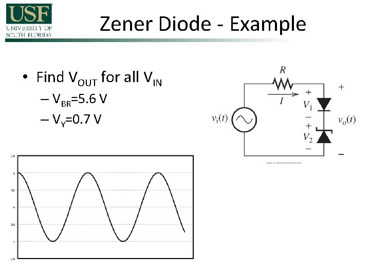
Zener Diode - Example • Find VOUT for all VIN – VBR=5. 6 V – VΥ=0. 7 V

Zener Diode - Example • Find VOUT for all VIN – VBR=5. 6 V – VΥ=0. 7 V

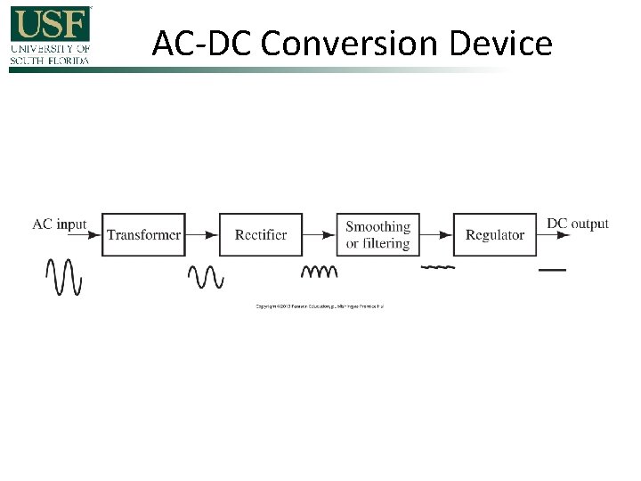
AC-DC Conversion Device

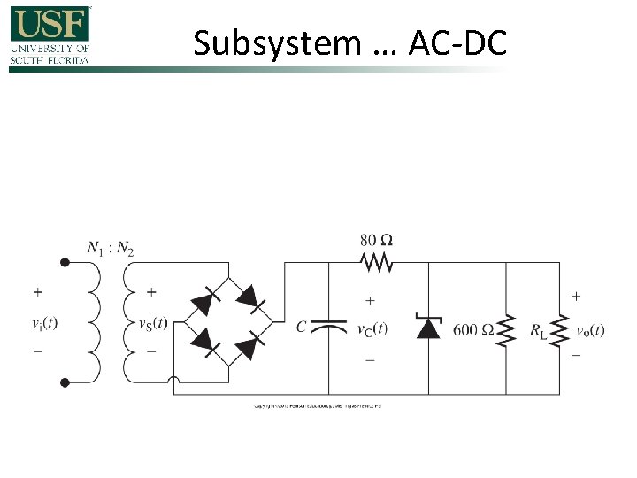
Subsystem … AC-DC

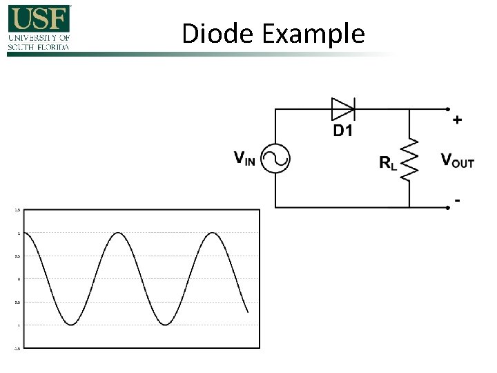
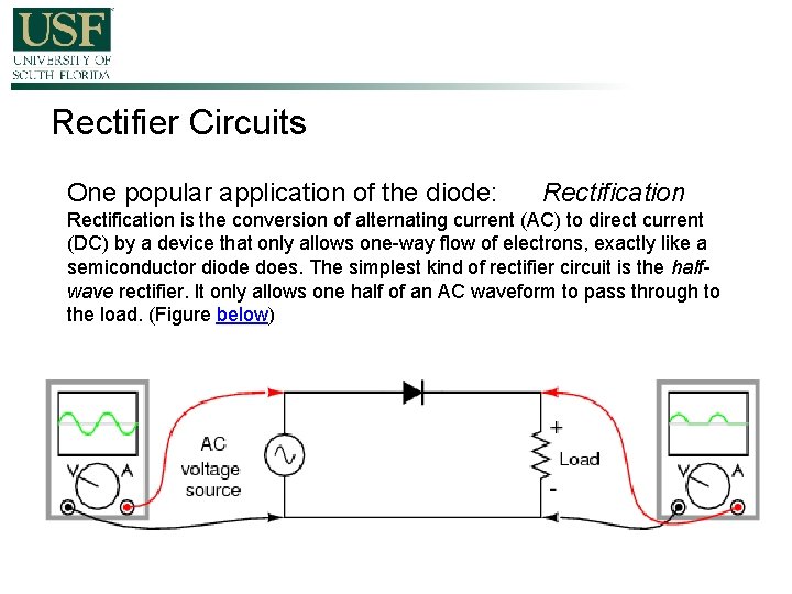
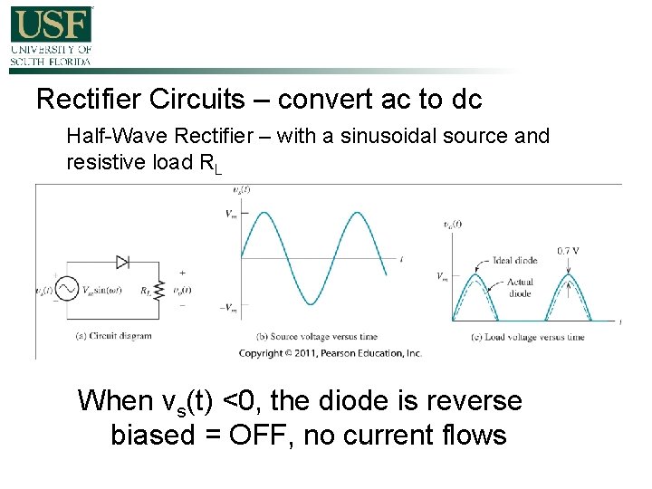
Rectifier Circuits One popular application of the diode: Rectification is the conversion of alternating current (AC) to direct current (DC) by a device that only allows one-way flow of electrons, exactly like a semiconductor diode does. The simplest kind of rectifier circuit is the halfwave rectifier. It only allows one half of an AC waveform to pass through to the load. (Figure below)

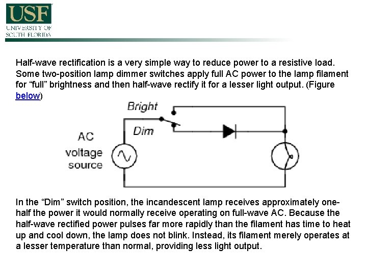
Half-wave rectification is a very simple way to reduce power to a resistive load. Some two-position lamp dimmer switches apply full AC power to the lamp filament for “full” brightness and then half-wave rectify it for a lesser light output. (Figure below) In the “Dim” switch position, the incandescent lamp receives approximately onehalf the power it would normally receive operating on full-wave AC. Because the half-wave rectified power pulses far more rapidly than the filament has time to heat up and cool down, the lamp does not blink. Instead, its filament merely operates at a lesser temperature than normal, providing less light output.

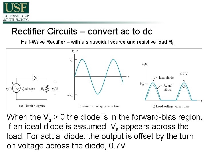
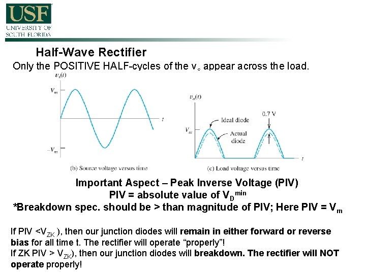
Rectifier Circuits – convert ac to dc Half-Wave Rectifier – with a sinusoidal source and resistive load RL When the Vs > 0 the diode is in the forward-bias region. If an ideal diode is assumed, Vs appears across the load. For actual diode, the output is offset by the turn on voltage across the diode, 0. 7 V

Rectifier Circuits – convert ac to dc Half-Wave Rectifier – with a sinusoidal source and resistive load RL When vs(t) <0, the diode is reverse biased = OFF, no current flows

Half-Wave Rectifier Only the POSITIVE HALF-cycles of the vs appear across the load. Important Aspect – Peak Inverse Voltage (PIV) PIV = absolute value of VDmin *Breakdown spec. should be > than magnitude of PIV; Here PIV = V m If PIV <VZK ), then our junction diodes will remain in either forward or reverse bias for all time t. The rectifier will operate “properly”! If ZK PIV > VZK), then our junction diodes will breakdown. The rectifier will NOT operate properly!

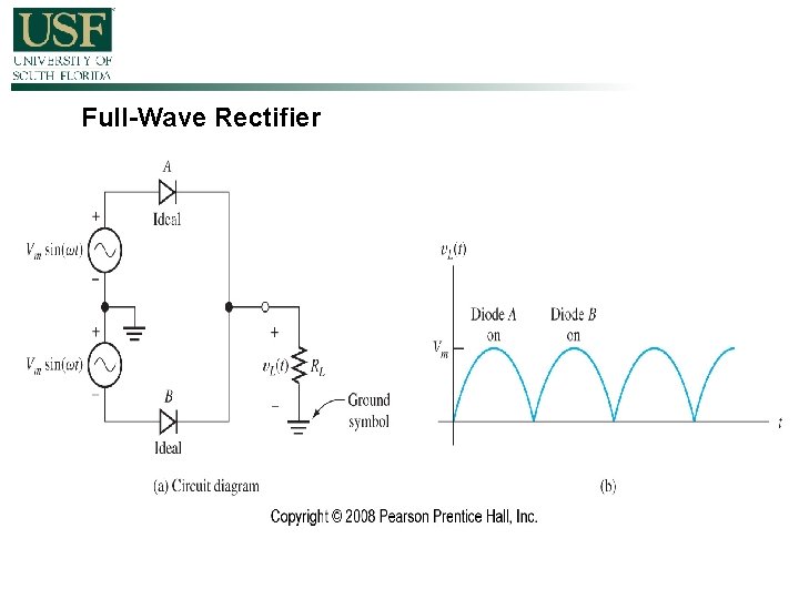
Full-Wave Rectifier

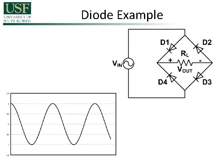
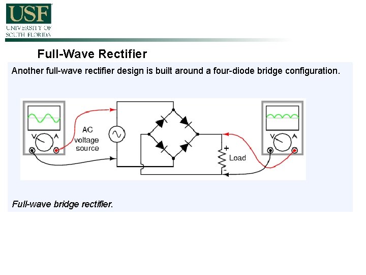
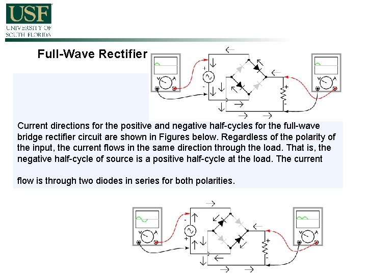
Full-Wave Rectifier Another full-wave rectifier design is built around a four-diode bridge configuration. Full-wave bridge rectifier.

Full-Wave Rectifier Current directions for the positive and negative half-cycles for the full-wave bridge rectifier circuit are shown in Figures below. Regardless of the polarity of the input, the current flows in the same direction through the load. That is, the negative half-cycle of source is a positive half-cycle at the load. The current flow is through two diodes in series for both polarities.