EE 4271 VLSI Design Dr Shiyan Hu Office
- Slides: 17

EE 4271 VLSI Design Dr. Shiyan Hu Office: EERC 731 Manufacturing Process -II Adapted and modified from Digital Integrated Circuits: A Design Perspective by Jan M. Rabaey, Anantha Chandrakasan, and Borivoje Nikolic. © EE 141 Digital Integrated Circuits 2 nd 1 Manufacturing

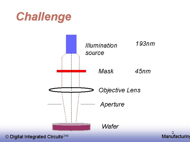
Challenge Illumination source Mask 193 nm 45 nm Objective Lens Aperture Wafer © EE 141 Digital Integrated Circuits 2 nd 2 Manufacturing

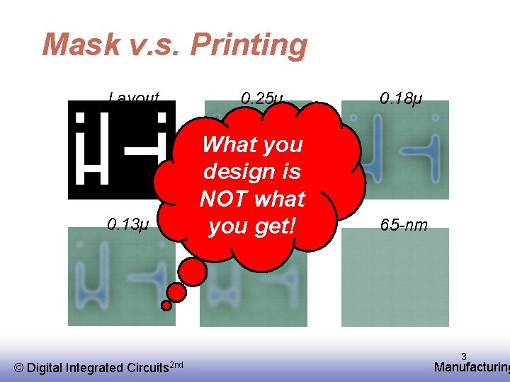
Mask v. s. Printing Layout 0. 13µ © EE 141 Digital Integrated Circuits 2 nd 0. 25µ What you design is NOT what you 90 -nm get! 0. 18µ 65 -nm 3 Manufacturing

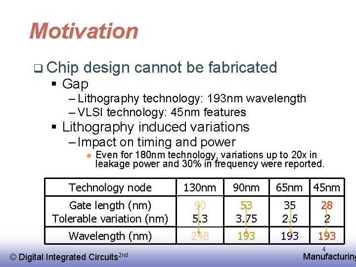
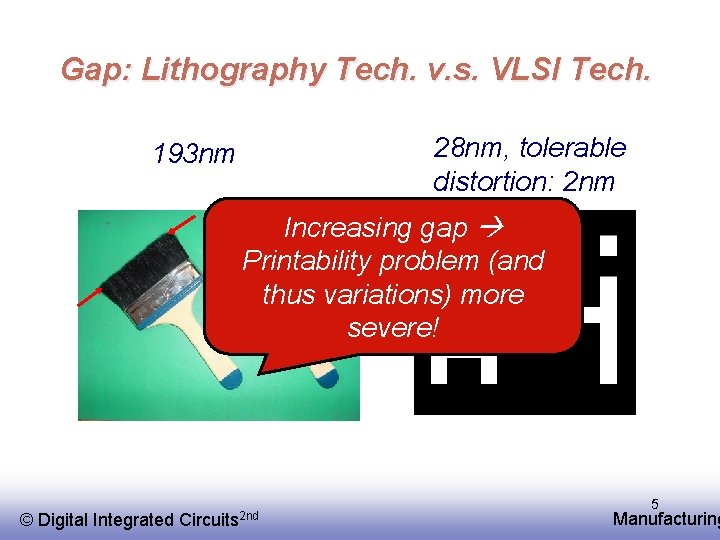
Motivation q Chip design cannot be fabricated § Gap – Lithography technology: 193 nm wavelength – VLSI technology: 45 nm features § Lithography induced variations – Impact on timing and power l Even for 180 nm technology, variations up to 20 x in leakage power and 30% in frequency were reported. Technology node 130 nm 90 nm Gate length (nm) Tolerable variation (nm) 90 5. 3 53 3. 75 35 2. 5 28 2 Wavelength (nm) 248 193 193 © EE 141 Digital Integrated Circuits 2 nd 65 nm 4 Manufacturing

Gap: Lithography Tech. v. s. VLSI Tech. 28 nm, tolerable distortion: 2 nm 193 nm Increasing gap Printability problem (and thus variations) more severe! © EE 141 Digital Integrated Circuits 2 nd 5 Manufacturing

Design Rules © EE 141 Digital Integrated Circuits 2 nd 6 Manufacturing

Design Rules Interface between designer and process engineer q Guidelines for constructing process masks q Unit dimension: Minimum line width § scalable design rules: lambda parameter § absolute dimensions (micron rules) q © EE 141 Digital Integrated Circuits 2 nd 7 Manufacturing

Lambda Rule q q Every distance in layout rules is specified by lambda Given a process, lambda is set to a specific value. § Process technology is defined using minimum line width. 0. 25 um technology means minimum line width is 0. 25 um. Lambda=minimum line width/2. § For a 0. 25 um process, lambda=0. 125 um In practice, scaling is often not linear. Industry usually uses micron rule and lambda rule is used only for prediction/estimation of the impact of technology scaling to a design. © EE 141 Digital Integrated Circuits 2 nd 8 Manufacturing

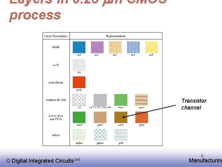
Layers in 0. 25 mm CMOS process Transistor channel © EE 141 Digital Integrated Circuits 2 nd 9 Manufacturing

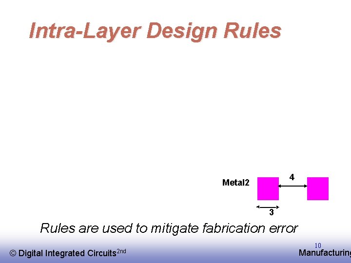
Intra-Layer Design Rules 4 Metal 2 3 Rules are used to mitigate fabrication error © EE 141 Digital Integrated Circuits 2 nd 10 Manufacturing

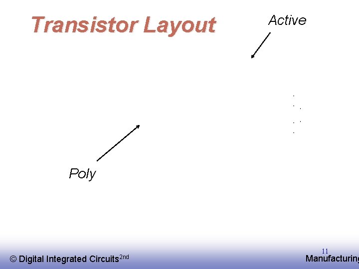
Transistor Layout Active Poly © EE 141 Digital Integrated Circuits 2 nd 11 Manufacturing

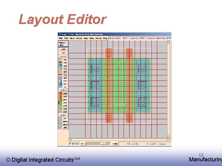
Layout Editor © EE 141 Digital Integrated Circuits 2 nd 12 Manufacturing

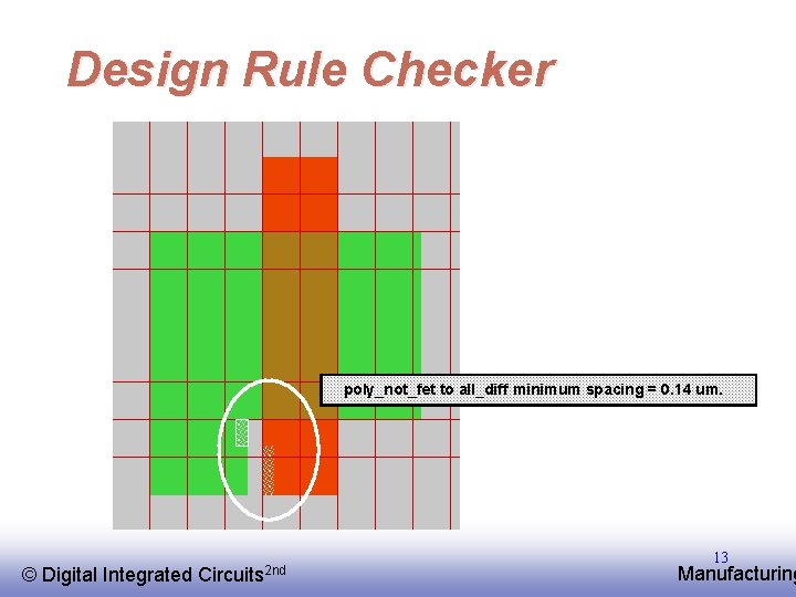
Design Rule Checker poly_not_fet to all_diff minimum spacing = 0. 14 um. © EE 141 Digital Integrated Circuits 2 nd 13 Manufacturing

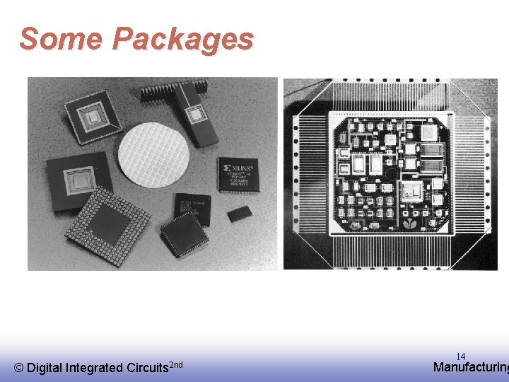
Some Packages © EE 141 Digital Integrated Circuits 2 nd 14 Manufacturing

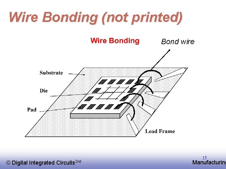
Wire Bonding (not printed) Bond wire © EE 141 Digital Integrated Circuits 2 nd 15 Manufacturing

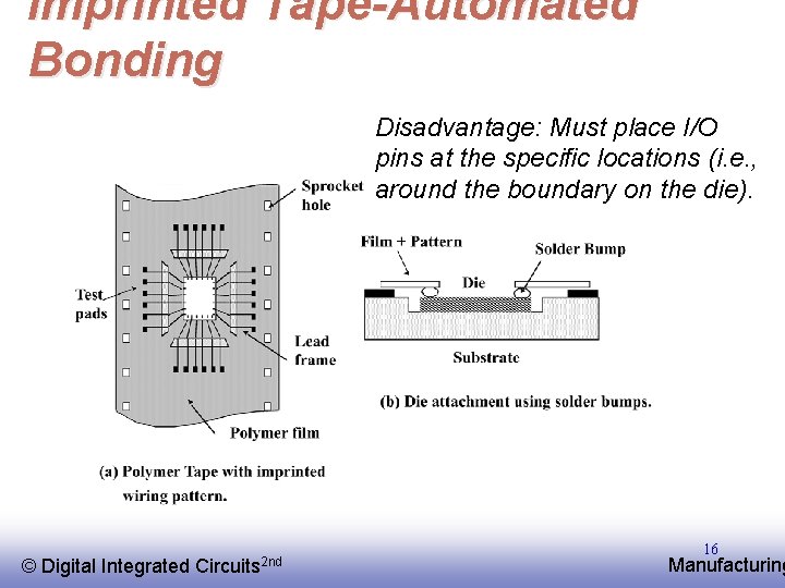
Imprinted Tape-Automated Bonding Disadvantage: Must place I/O pins at the specific locations (i. e. , around the boundary on the die). © EE 141 Digital Integrated Circuits 2 nd 16 Manufacturing

Flip-Chip Bonding q Flip-Chip places connection across the chip rather than around boundary. q The bond wire is replaced with solder bump balls directly placed on the die surface q Chip is flipped upside down q Carefully align to package q Heat to melt solder bump balls © EE 141 Digital Integrated Circuits 2 nd 17 Manufacturing