EE 4271 VLSI Design Fall 2011 Static Timing
- Slides: 18

EE 4271 VLSI Design, Fall 2011 Static Timing Analysis and Gate Sizing Optimization

Delay Evaluation • 1. Gate delay • 2. Interconnect delay 2020/9/9 Circuit Delay PJF- 2

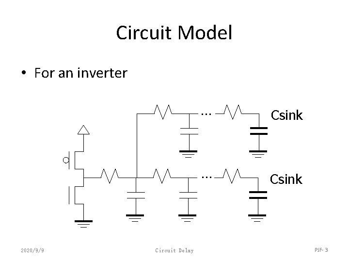
Circuit Model • For an inverter 2020/9/9 Circuit Delay … Csink PJF- 3

Gate Resistance • Pull-up and pull-down resistors are not a constant. Which value should we choose? • Gate delay also depends on its input signal 2020/9/9 Circuit Delay PJF- 4

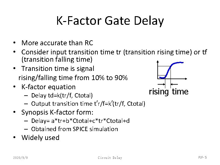
K-Factor Gate Delay • More accurate than RC • Consider input transition time tr (transition rising time) or tf (transition falling time) • Transition time is signal rising/falling time from 10% to 90% • K-factor equation – Delay td=k(tr/f, Ctotal) – Output transition time t’r/f=k’(tr/f, Ctotal) rising time • Synopsis K-factor form: – Delay= a*tr+b*Ctotal+c*tr*Ctotal+d – Obtained from SPICE simulation • Widely used 2020/9/9 Circuit Delay PJF- 5

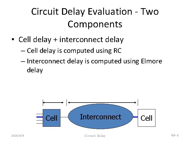
Circuit Delay Evaluation - Two Components • Cell delay + interconnect delay – Cell delay is computed using RC – Interconnect delay is computed using Elmore delay Cell 2020/9/9 Interconnect Circuit Delay Cell PJF- 6

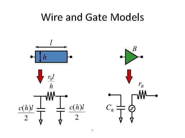
Wire and Gate Models 7

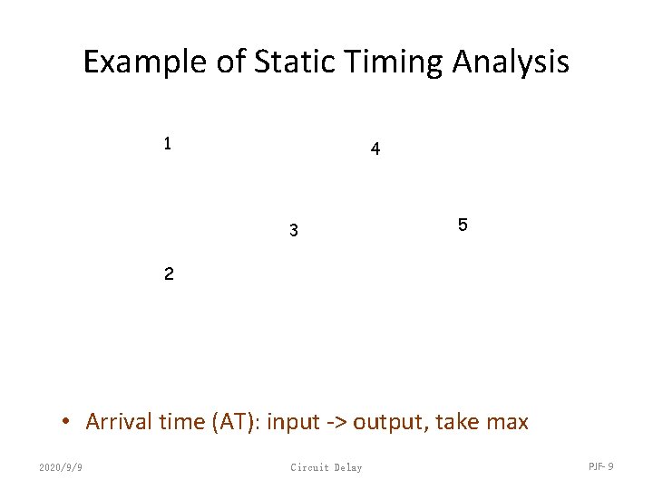
Step by Step n n Model combinational circuit using the previous slide Starting from primary input gates, compute the arrival time (AT) at each gate, i. e. , compute gate delay and interconnect delay In order to compute the AT at a gate, the ATs of all its input gates need to be computed Repeat the above process until the ATs at all primary output gates are computed 2020/9/9 Circuit Delay PJF- 8

Example of Static Timing Analysis 1 4 3 5 2 • Arrival time (AT): input -> output, take max 2020/9/9 Circuit Delay PJF- 9

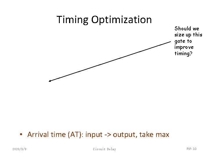
Timing Optimization Should we size up this gate to improve timing? • Arrival time (AT): input -> output, take max 2020/9/9 Circuit Delay PJF- 10

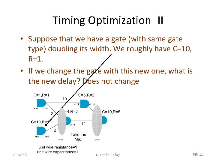
Timing Optimization- II • Suppose that we have a gate (with same gate type) doubling its width. We roughly have C=10, R=1. • If we change the gate with this new one, what is the new delay? Does not change 2020/9/9 Circuit Delay PJF- 11

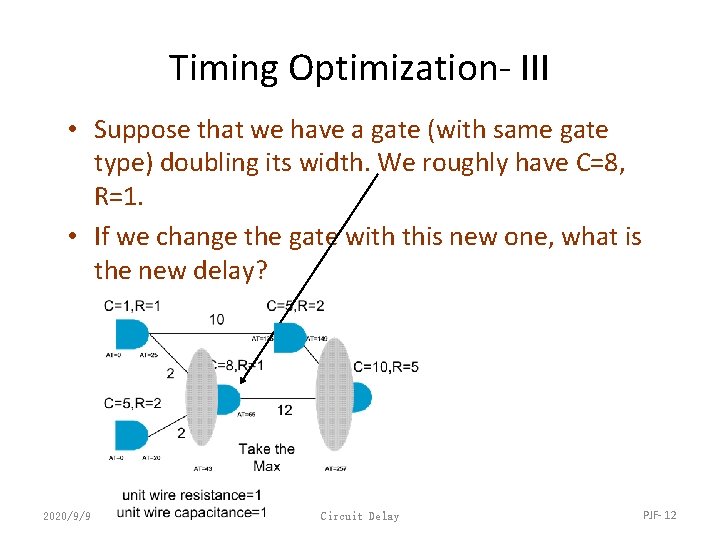
Timing Optimization- III • Suppose that we have a gate (with same gate type) doubling its width. We roughly have C=8, R=1. • If we change the gate with this new one, what is the new delay? 2020/9/9 Circuit Delay PJF- 12

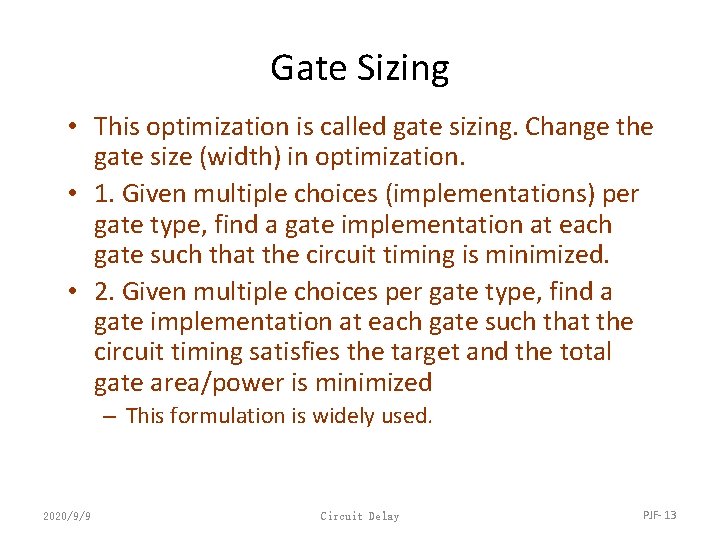
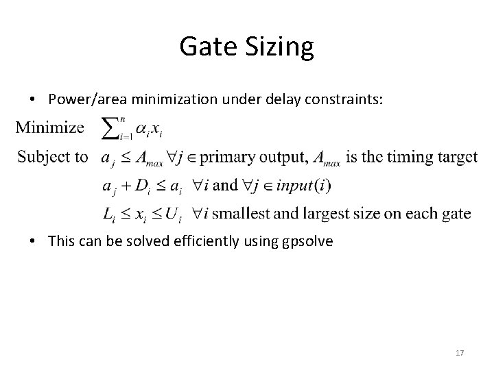
Gate Sizing • This optimization is called gate sizing. Change the gate size (width) in optimization. • 1. Given multiple choices (implementations) per gate type, find a gate implementation at each gate such that the circuit timing is minimized. • 2. Given multiple choices per gate type, find a gate implementation at each gate such that the circuit timing satisfies the target and the total gate area/power is minimized – This formulation is widely used. 2020/9/9 Circuit Delay PJF- 13

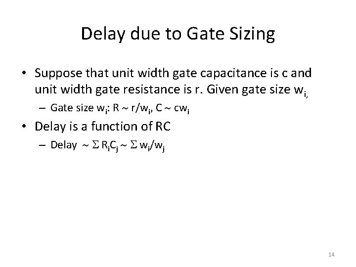
Delay due to Gate Sizing • Suppose that unit width gate capacitance is c and unit width gate resistance is r. Given gate size wi, – Gate size wi: R r/wi, C cwi • Delay is a function of RC – Delay Ri. Cj wi/wj 14

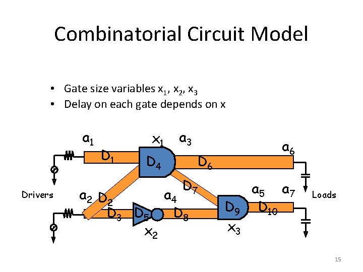
Combinatorial Circuit Model • Gate size variables x 1, x 2, x 3 • Delay on each gate depends on x a 1 Drivers D 1 x 1 a 3 D 4 a 6 D 7 a 2 D 2 a 4 D 3 D 5 D 8 x 2 D 9 x 3 a 5 a 7 D 10 Loads 15

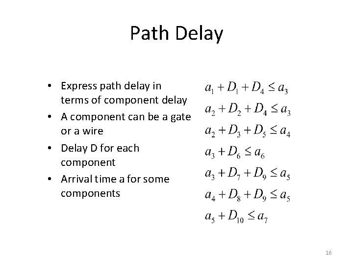
Path Delay • Express path delay in terms of component delay • A component can be a gate or a wire • Delay D for each component • Arrival time a for some components 16

Gate Sizing • Power/area minimization under delay constraints: • This can be solved efficiently using gpsolve 17

Gate Sizing using GPSOLVE • Follow the steps in gatesizing. m for the example in the slides of timing analysis and optimization 18