Digital Electronics 1 ET 255 Introduction to Digital
- Slides: 29

Digital Electronics 1 ET 255 Introduction to Digital Concepts Chapter 1

Digital and Analog Quantities • Analog quantity is any value that, when measured, changes over a period of time – It encompasses an infinite number of values over time – No measure is to small to be included – Gradual changes – Example: A sinusoidal wave • Digital quantity are discrete values represented over time – A precise value is represented at a given moment of time – All values in between those steps in time are ignored

Digital and Analog Quantities • Digital has the advantage over Analog – it is easier to transmit and decode a digital signal than an Analog one – Noise has less impact on a digital signal – Requires less power to transmit digital than Analog

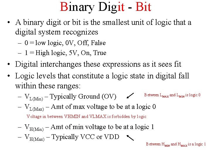
Binary Digit - Bit • A binary digit or bit is the smallest unit of logic that a digital system recognizes – 0 = low logic, 0 V, Off, False – 1 = High logic, 5 V, On, True • Digital interchanges these expressions as it sees fit • Logic levels that constitute a logic state in digital fall within these ranges: Between L – VL(Min) – Typically Ground (OV) – VL(Max) – Amt of max voltage to be at a logic 0 MAX and LMIN is logic 0 Voltage in between VHMIN and VLMAX is forbidden by logic – VH(Min) – Amt of min voltage to be at a logic 1 – VH(Max) – Typically VCC or VDD Between HMIN and HMAX is a logic 1

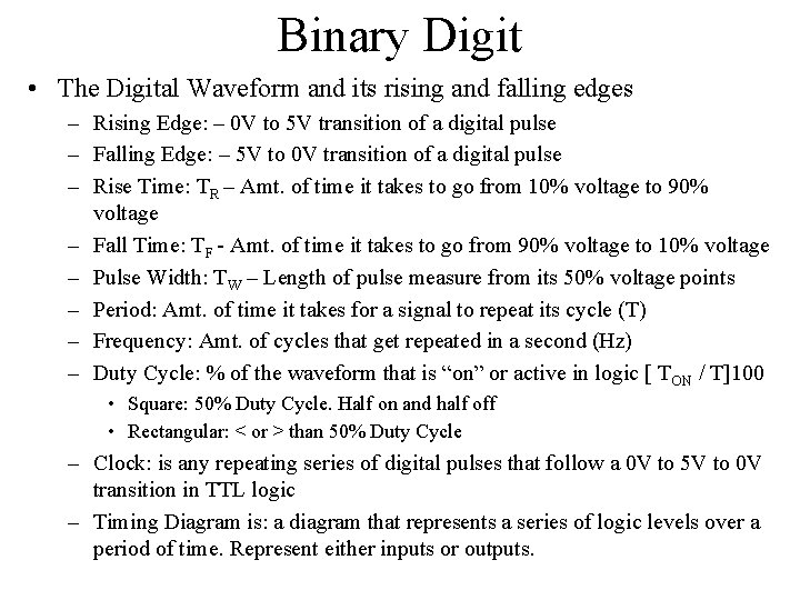
Binary Digit • The Digital Waveform and its rising and falling edges – Rising Edge: – 0 V to 5 V transition of a digital pulse – Falling Edge: – 5 V to 0 V transition of a digital pulse – Rise Time: TR – Amt. of time it takes to go from 10% voltage to 90% voltage – Fall Time: TF - Amt. of time it takes to go from 90% voltage to 10% voltage – Pulse Width: TW – Length of pulse measure from its 50% voltage points – Period: Amt. of time it takes for a signal to repeat its cycle (T) – Frequency: Amt. of cycles that get repeated in a second (Hz) – Duty Cycle: % of the waveform that is “on” or active in logic [ TON / T]100 • Square: 50% Duty Cycle. Half on and half off • Rectangular: < or > than 50% Duty Cycle – Clock: is any repeating series of digital pulses that follow a 0 V to 5 V to 0 V transition in TTL logic – Timing Diagram is: a diagram that represents a series of logic levels over a period of time. Represent either inputs or outputs.

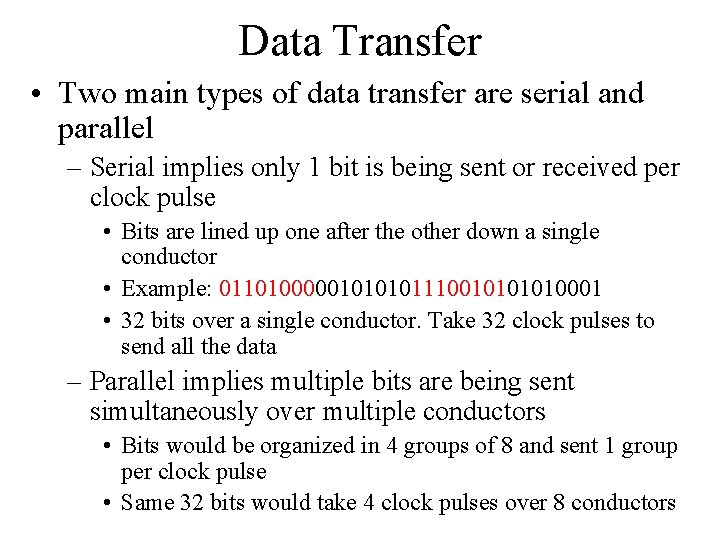
Data Transfer • Two main types of data transfer are serial and parallel – Serial implies only 1 bit is being sent or received per clock pulse • Bits are lined up one after the other down a single conductor • Example: 011010000010111001010001 • 32 bits over a single conductor. Take 32 clock pulses to send all the data – Parallel implies multiple bits are being sent simultaneously over multiple conductors • Bits would be organized in 4 groups of 8 and sent 1 group per clock pulse • Same 32 bits would take 4 clock pulses over 8 conductors

Logic Gates • Logic gates are IC’s (Integrated Circuits) that follow the rules and laws of Boolean Algebra – Main logic gates are: AND, OR, NOT, Ex-OR – Sub gates include: NAND, NOR, Ex-NOR • The following slides will break down the gates, their TTL family number, Truth Table, and pin layout • IT IS IMPORTANT to learn these gates. All of digital is tied to the logical theory of these chips

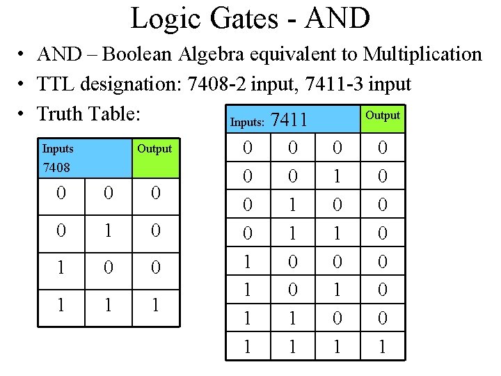
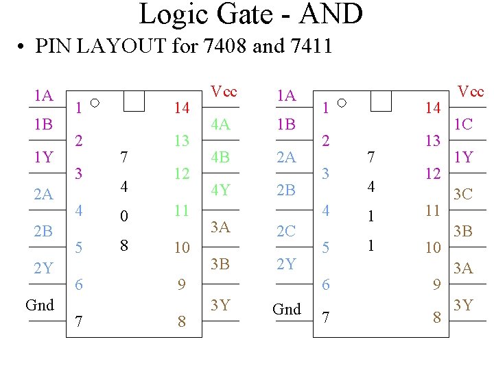
Logic Gates - AND • AND – Boolean Algebra equivalent to Multiplication • TTL designation: 7408 -2 input, 7411 -3 input Output • Truth Table: Inputs: 7411 Inputs Output 7408 0 0 1 1 1 0 0 1 1 0 1 0 1 0 0 0 0 1

Logic Gate - AND • PIN LAYOUT for 7408 and 7411 1 A 1 B 1 Y 2 A 2 B 2 Y Gnd 1 14 2 13 3 4 5 6 7 7 4 12 0 11 8 10 Vcc 1 A 4 A 1 B 4 B 2 A 4 Y 2 B 3 A 3 B 14 2 13 3 4 2 C 2 Y 9 8 1 5 6 3 Y Gnd 7 7 4 12 1 11 1 10 9 8 Vcc 1 C 1 Y 3 C 3 B 3 A 3 Y

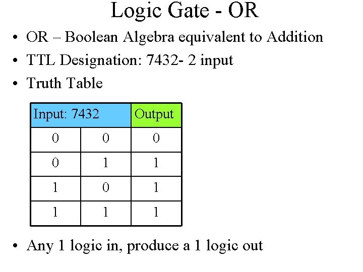
Logic Gate - OR • OR – Boolean Algebra equivalent to Addition • TTL Designation: 7432 - 2 input • Truth Table Input: 7432 Output 0 0 1 1 1 0 1 1 • Any 1 logic in, produce a 1 logic out

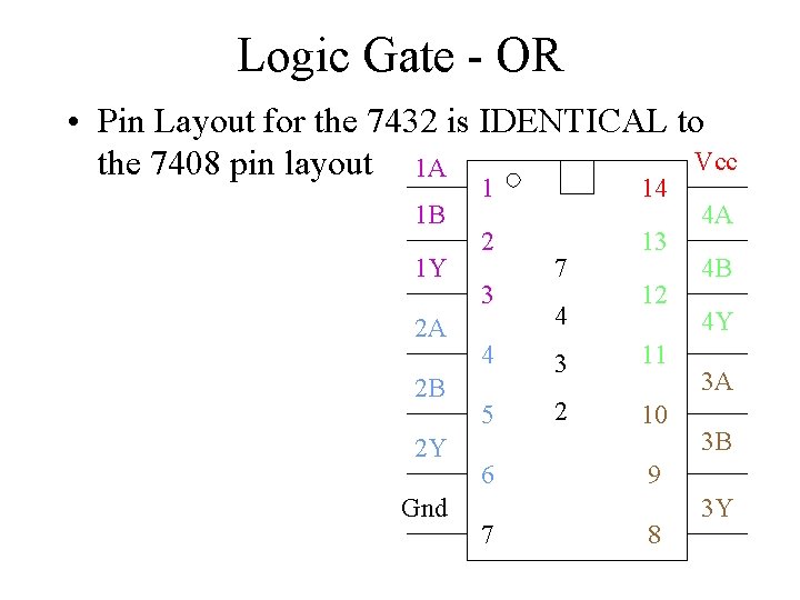
Logic Gate - OR • Pin Layout for the 7432 is IDENTICAL to Vcc the 7408 pin layout 1 A 1 B 1 Y 2 A 2 B 2 Y Gnd 1 14 2 13 3 7 4 12 4 3 11 5 2 10 6 7 4 A 4 B 4 Y 3 A 3 B 9 8 3 Y

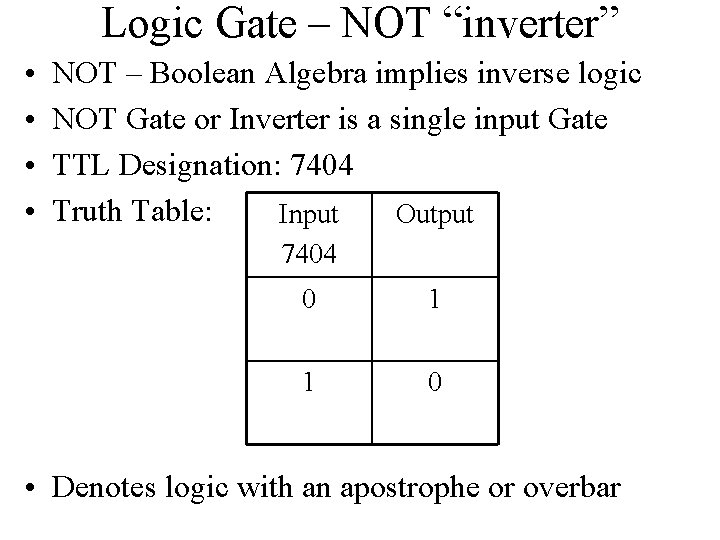
Logic Gate – NOT “inverter” • • NOT – Boolean Algebra implies inverse logic NOT Gate or Inverter is a single input Gate TTL Designation: 7404 Truth Table: Input Output 7404 0 1 1 0 • Denotes logic with an apostrophe or overbar

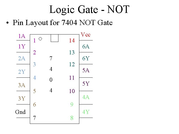
Logic Gate - NOT • Pin Layout for 7404 NOT Gate 1 A 1 Y 2 A 2 Y 3 A 3 Y Gnd 1 14 2 13 3 7 4 12 4 0 11 5 4 10 6 7 Vcc 6 A 6 Y 5 A 5 Y 4 A 9 8 4 Y

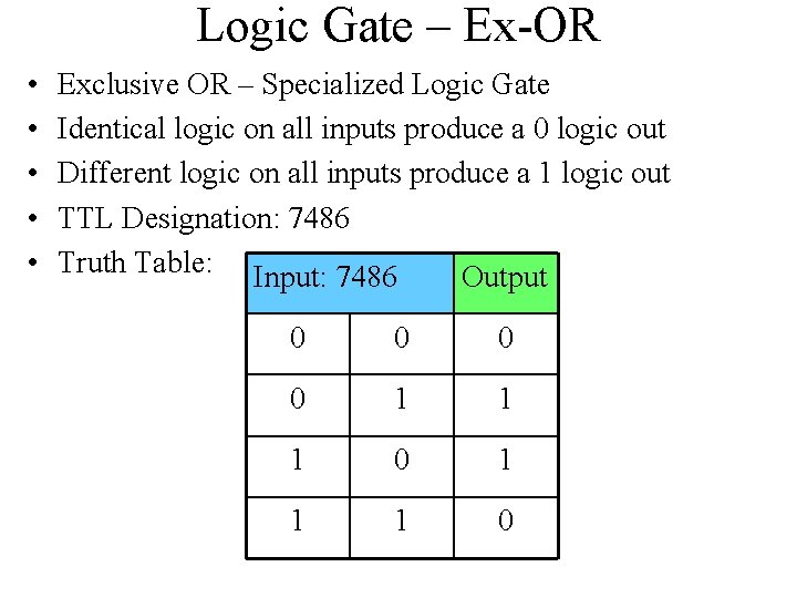
Logic Gate – Ex-OR • • • Exclusive OR – Specialized Logic Gate Identical logic on all inputs produce a 0 logic out Different logic on all inputs produce a 1 logic out TTL Designation: 7486 Truth Table: Input: 7486 Output 0 0 1 1 1 0

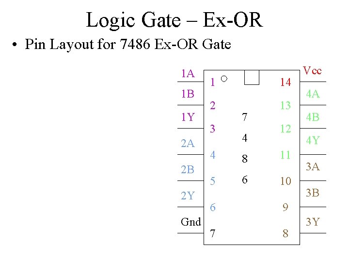
Logic Gate – Ex-OR • Pin Layout for 7486 Ex-OR Gate 1 A 1 B 1 Y 2 A 2 B 2 Y Gnd 1 14 2 13 3 7 4 12 4 8 11 5 6 10 6 7 Vcc 4 A 4 B 4 Y 3 A 3 B 9 8 3 Y

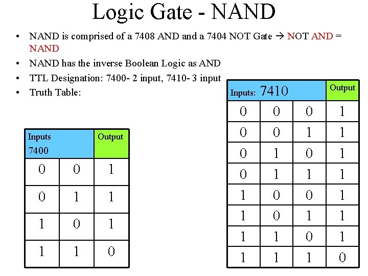
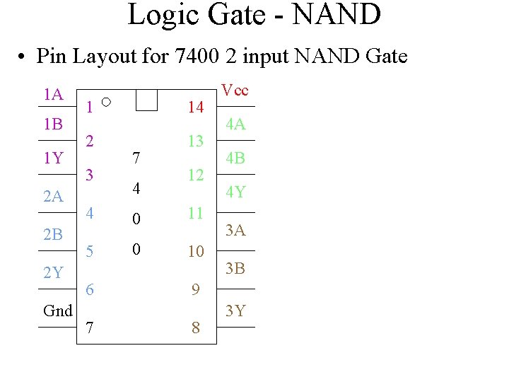
Logic Gate - NAND • NAND is comprised of a 7408 AND and a 7404 NOT Gate NOT AND = NAND • NAND has the inverse Boolean Logic as AND • TTL Designation: 7400 - 2 input, 7410 - 3 input Output Inputs: 7410 • Truth Table: Inputs Output 7400 0 0 1 1 1 0 0 0 1 1 0 1 0 1 1 1 1 1 0

Logic Gate - NAND • Pin Layout for 7400 2 input NAND Gate 1 A 1 B 1 Y 2 A 2 B 2 Y Gnd 1 14 2 13 3 7 4 12 4 0 11 5 0 10 6 7 Vcc 4 A 4 B 4 Y 3 A 3 B 9 8 3 Y

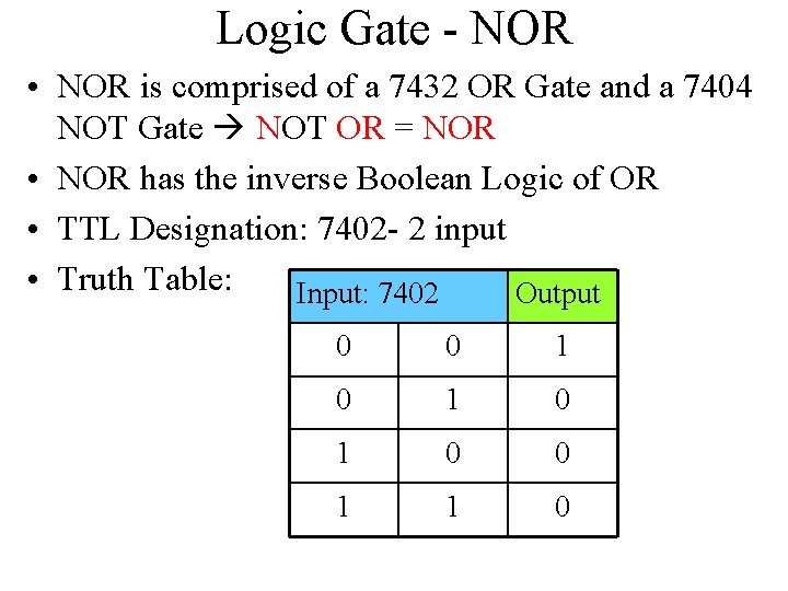
Logic Gate - NOR • NOR is comprised of a 7432 OR Gate and a 7404 NOT Gate NOT OR = NOR • NOR has the inverse Boolean Logic of OR • TTL Designation: 7402 - 2 input • Truth Table: Input: 7402 Output 0 0 1 0 1 0 0 1 1 0

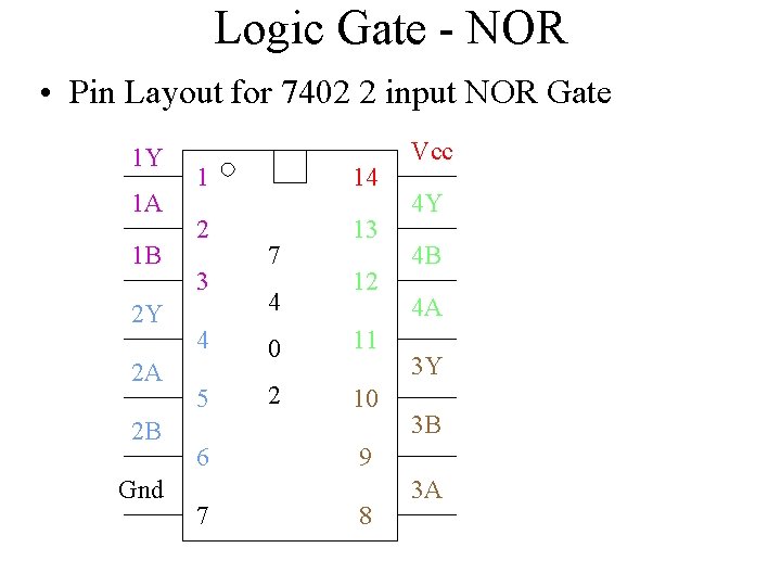
Logic Gate - NOR • Pin Layout for 7402 2 input NOR Gate 1 Y 1 A 1 B 2 Y 2 A 2 B Gnd 1 14 2 13 3 7 4 12 4 0 11 5 2 10 6 7 Vcc 4 Y 4 B 4 A 3 Y 3 B 9 8 3 A

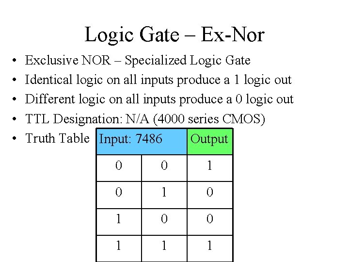
Logic Gate – Ex-Nor • • • Exclusive NOR – Specialized Logic Gate Identical logic on all inputs produce a 1 logic out Different logic on all inputs produce a 0 logic out TTL Designation: N/A (4000 series CMOS) Truth Table Input: 7486 Output 0 0 1 0 1 0 0 1 1 1

Digital Applications • Magnitude Comparators, Arithmetic, Code Conversion, Encoding, Decoding, Data Selection, Storage, and Counting – Magnitude Comparators: Compare two words and mathematically chooses if one is greater than, equal to, or less than the other – Arithmetic: Addition, Subtraction, Multiplication, and Division – Code Conversion: Allows for one binary code to be converted to another (Binary Gray) – Encoding / Decoding: allows for inputs to be altered to unique outputs and be reverted back to the original

Digital Applications – Data Selection: Allows for Multiplexed and Demultiplexed lines to be selected as an output or input – Storage: Registers and flip flops offer memory devices to hold a logical state – Counting: Utilizes Flip Flops to increment coded binary systems into a synchronized clocked event

IC Packages • DIP – Dual Inline Package • SMT – Surface Mount Technology – SOIC: small outline integrated circuit – PLCC: plastic leaded chip carrier – LCCC: leadless ceramic chip carrier – FP: flat pack – SSOP: shrink small outline package – TSSOP: thin shrink small outline package – TVSOP: thin very small outline package

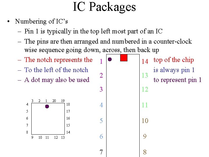
IC Packages • Numbering of IC’s – Pin 1 is typically in the top left most part of an IC – The pins are then arranged and numbered in a counter-clock wise sequence going down, across, then back up – The notch represents the 1 14 top of the chip – To the left of the notch is always pin 1 2 13 – A dot may also be used to represent pin 1 7 3 12 4 3 2 1 20 19 4 18 4 11 0 5 17 6 16 7 15 8 14 9 10 11 12 13 5 2 10 6 9 7 8

IC Packages • Complexity Classifications for Fixed Function IC – SSI: Small Scale Integration – up to 12 equivalent gate circuits (logic gates) – MSI: Medium Scale Integration – from 12 to 99 equivalent gates on a chip (encoder, decoder, register) – LSI: Large Scale Integration – 100 to 9999 equivalent gates (memory) – VLSI: Very Large Scale Integration – 10, 000 to 99, 999 equivalent gates – ULSI: Ultra Large Scale Integration – 100, 000 gates or larger (CPU’s, High Capacity Memory)

Programmable Logic Devices • 3 major categories: SPLD, CPLD, and FPGA – SPLD: Simple Programmable Logic Devices • PROM – EPROM and EEPROM: Programmable Read Only Memory (Erasable and Electrically Erasable) • PAL: Programmable Array Logic • PLA: Programmable Array Logic • GAL: Gate Array Logic – CPLD: Complex Programmable Logic Devices • Macrocell • Programmable Interconnect • I/O Pads – FPGA: Field Programmable Gate Array

Test Equipment • Oscilloscope: Device that visually displays voltage or current over time • Logic Analyzer: Device that allows multiple digital inputs and outputs to be monitored simultaneously over time • Logic Probe: Detects the presence of a logic state • Logic Pulsar: Injects a logic state in a circuit • Function Generator: Produces Oscillations • Digital Multi-meter: Measures Current or Voltage for AC/DC as well as measure Resistance

Review of Week 2 • Chapter 2: Number Systems – – – Review the base 10 Decimal system Learn Binary: Base 2 system Learn to convert Base 10 to Base 2; Base 2 to Base 10 Learn to convert Base 10 fractions into Base 2 Learn the rules of Base 2 Addition, Subtraction, Multiplication, and Division – Learn how to 1’s and 2’s complement base 2 numbers – Learn how to represent Base 2 numbers in sign magnitude form – Learn how to add, subtract, multiply and divide signed numbers

Review of Week 2 – Learn Hexadecimal: Base 16 system – Learn Base 2 to Base 16; Base 16 to Base 2 conversion – Learn Base 10 to Base 16; Base 16 to Base 10 conversion – Learn Base 16 Addition and Subtraction – Learn Octal: Base 8 System – Learn Base 8 to Base 10; Base 10 to Base 8 conversion – Learn Base 8 to Base 2; Base 2 to Base 8 conversion – Learn BCD: Binary Coded Decimal; Add BCD numbers – Learn Gray code, Alphanumeric, and ASCII