CMOS differential amplifier with resistive load limitations 1
- Slides: 28

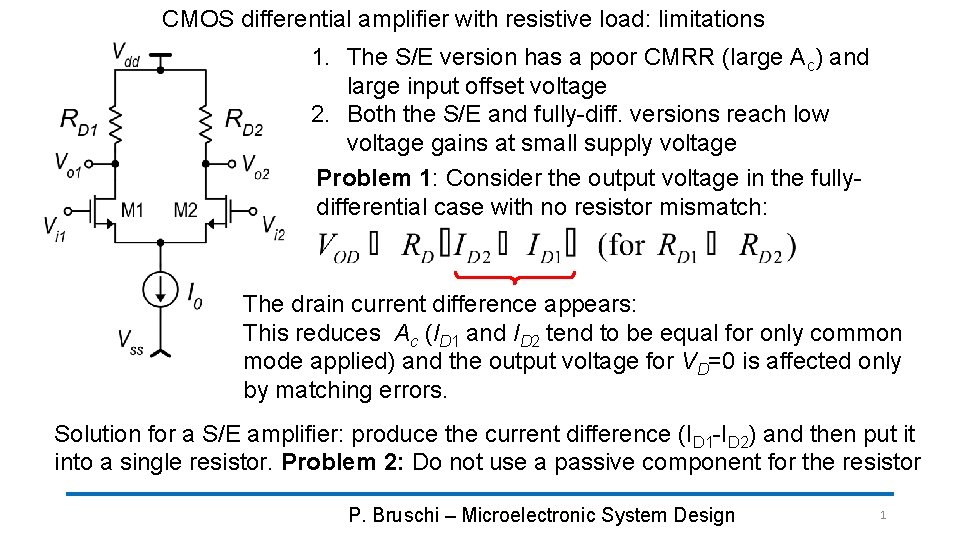
CMOS differential amplifier with resistive load: limitations 1. The S/E version has a poor CMRR (large Ac) and large input offset voltage 2. Both the S/E and fully-diff. versions reach low voltage gains at small supply voltage Problem 1: Consider the output voltage in the fullydifferential case with no resistor mismatch: The drain current difference appears: This reduces Ac (ID 1 and ID 2 tend to be equal for only common mode applied) and the output voltage for VD=0 is affected only by matching errors. Solution for a S/E amplifier: produce the current difference (ID 1 -ID 2) and then put it into a single resistor. Problem 2: Do not use a passive component for the resistor P. Bruschi – Microelectronic System Design 1

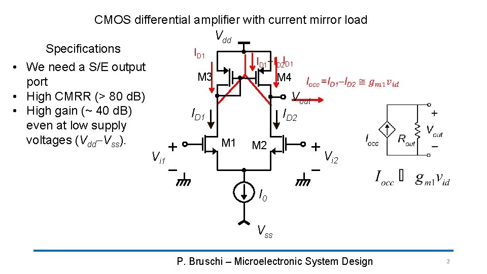
CMOS differential amplifier with current mirror load Vdd Specifications ID 1+ID 2 ID 1 • We need a S/E output port • High CMRR (> 80 d. B) • High gain (~ 40 d. B) even at low supply voltages (Vdd-Vss). M 3 M 4 Vout ID 1 ID 2 M 1 Vi 1 M 2 Vi 2 I 0 Vss P. Bruschi – Microelectronic System Design 2

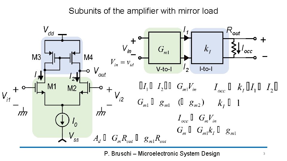
Subunits of the amplifier with mirror load I 1 Rout Iocc Vin I 1 I 2 V-to-I I 2 I-to-I P. Bruschi – Microelectronic System Design 3

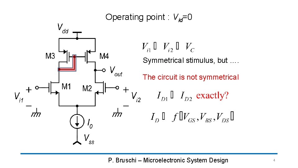
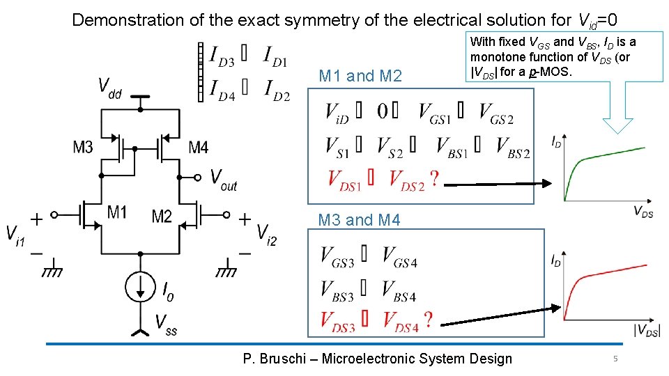
Operating point : Vid=0 Symmetrical stimulus, but …. The circuit is not symmetrical P. Bruschi – Microelectronic System Design 4

Demonstration of the exact symmetry of the electrical solution for Vid=0 M 1 and M 2 With fixed VGS and VBS, ID is a monotone function of VDS (or |VDS| for a p-MOS. M 3 and M 4 P. Bruschi – Microelectronic System Design 5

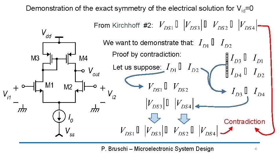
Demonstration of the exact symmetry of the electrical solution for Vid=0 From Kirchhoff #2: We want to demonstrate that: Proof by contradiction: Let us suppose: Contradiction P. Bruschi – Microelectronic System Design 6

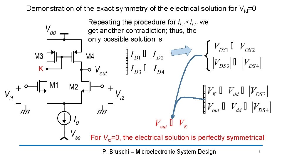
Demonstration of the exact symmetry of the electrical solution for Vid=0 Repeating the procedure for ID 1<ID 2 we get another contradiction; thus, the only possible solution is: K For Vid=0, the electrical solution is perfectly symmetrical P. Bruschi – Microelectronic System Design 7

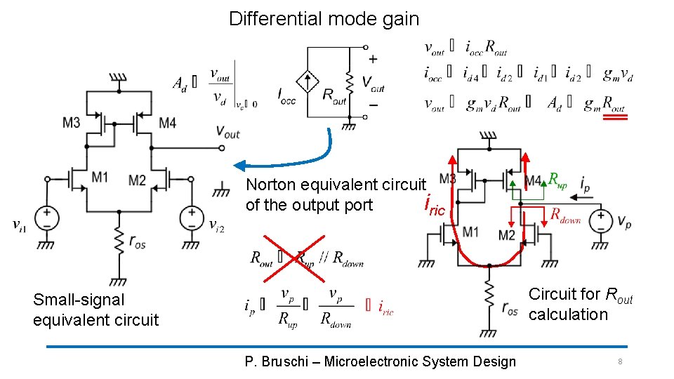
Differential mode gain Norton equivalent circuit iric of the output port Circuit for Rout calculation Small-signal equivalent circuit P. Bruschi – Microelectronic System Design 8

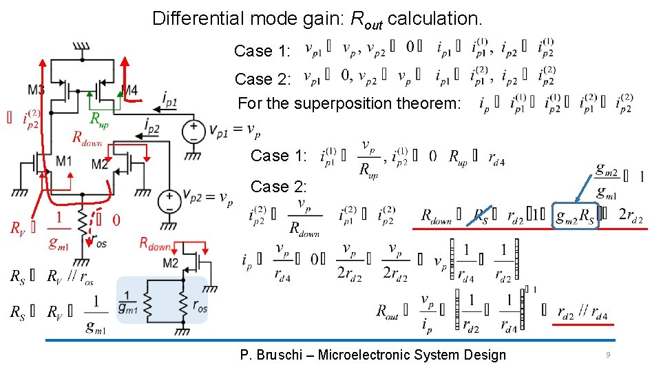
Differential mode gain: Rout calculation. Case 1: Case 2: For the superposition theorem: Case 1: Case 2: P. Bruschi – Microelectronic System Design 9

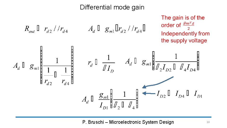
Differential mode gain P. Bruschi – Microelectronic System Design 10

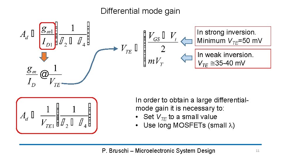
Differential mode gain In strong inversion. Minimum VTE=50 m. V In order to obtain a large differentialmode gain it is necessary to: • Set VTE to a small value • Use long MOSFETs (small l) P. Bruschi – Microelectronic System Design 11

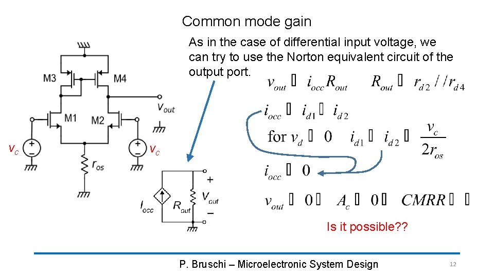
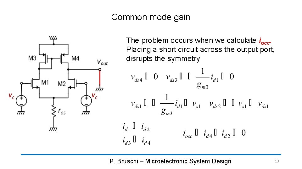
Common mode gain As in the case of differential input voltage, we can try to use the Norton equivalent circuit of the output port. vc vc Is it possible? ? P. Bruschi – Microelectronic System Design 12

Common mode gain The problem occurs when we calculate iocc. Placing a short circuit across the output port, disrupts the symmetry: vc vc P. Bruschi – Microelectronic System Design 13

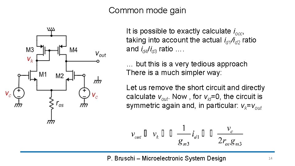
Common mode gain It is possible to exactly calculate iocc, taking into account the actual id 1/id 2 ratio and id 4/id 3 ratio …. vk vc … but this is a very tedious approach There is a much simpler way: vc Let us remove the short circuit and directly calculate vout. Now , for vid=0, the circuit is symmetric again and, in particular: vk=vout P. Bruschi – Microelectronic System Design 14

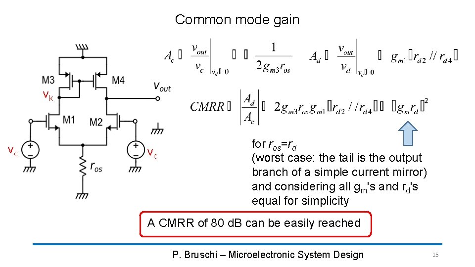
Common mode gain vk vc vc for ros=rd (worst case: the tail is the output branch of a simple current mirror) and considering all gm's and rd's equal for simplicity A CMRR of 80 d. B can be easily reached P. Bruschi – Microelectronic System Design 15

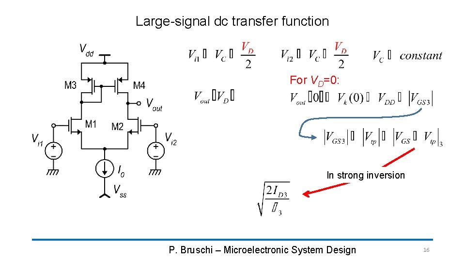
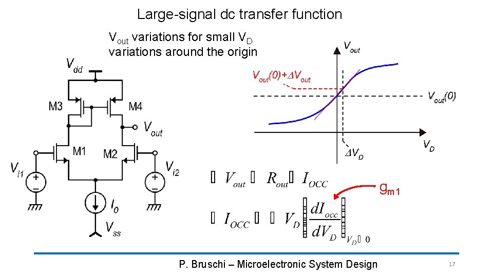
Large-signal dc transfer function For VD=0: In strong inversion P. Bruschi – Microelectronic System Design 16

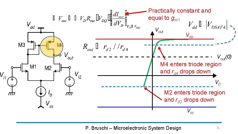
Large-signal dc transfer function Vout variations for small VD variations around the origin gm 1 P. Bruschi – Microelectronic System Design 17

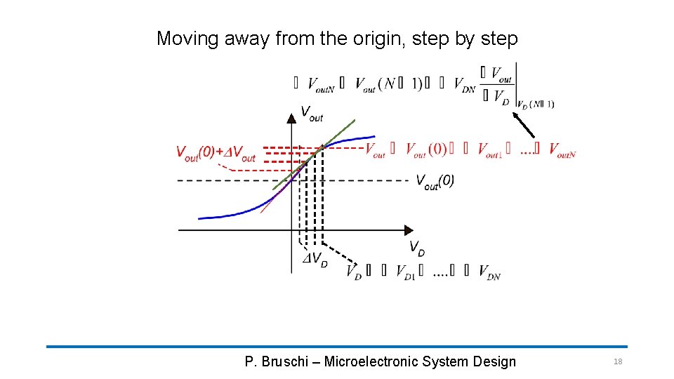
Moving away from the origin, step by step P. Bruschi – Microelectronic System Design 18

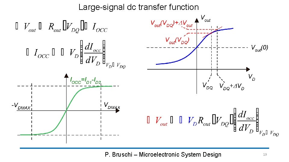
Large-signal dc transfer function P. Bruschi – Microelectronic System Design 19

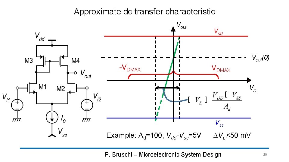
Approximate dc transfer characteristic Vout Vdd Vout(0) -VDMAX VD Vss Example: Ad=100, Vdd-Vss=5 V DVD<50 m. V P. Bruschi – Microelectronic System Design 20

Practically constant and equal to gm 1 Vout Vdd Vout(0) M 4 enters triode region and rd 4 drops down VD M 2 enters triode region and rd 2 drops down Vss P. Bruschi – Microelectronic System Design 21

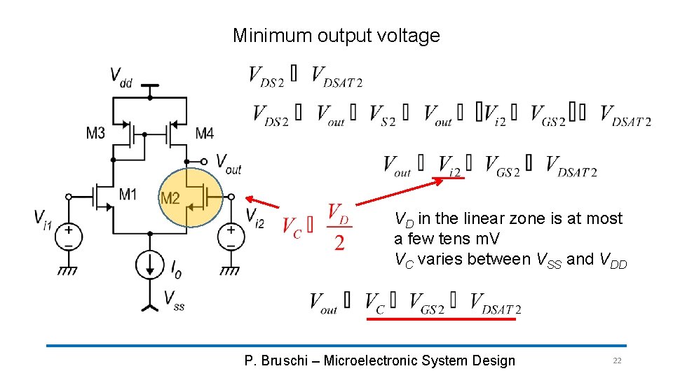
Minimum output voltage VD in the linear zone is at most a few tens m. V VC varies between VSS and VDD P. Bruschi – Microelectronic System Design 22

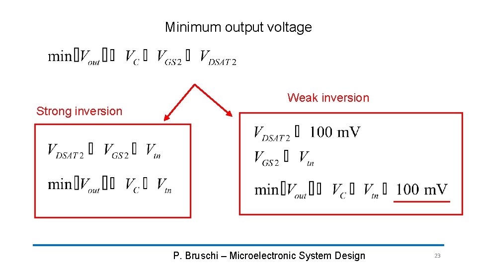
Minimum output voltage Weak inversion Strong inversion P. Bruschi – Microelectronic System Design 23

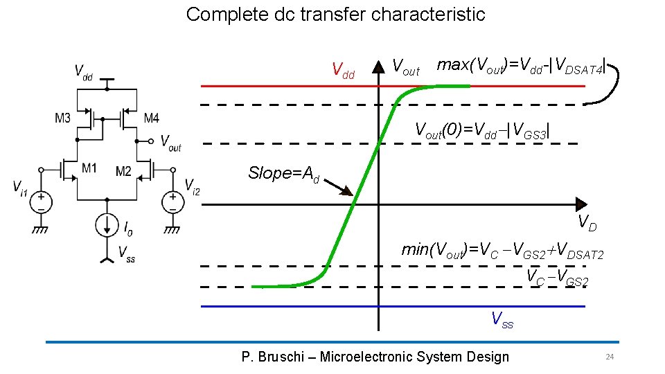
Complete dc transfer characteristic Vdd Vout max(Vout)=Vdd-|VDSAT 4| Vout(0)=Vdd-|VGS 3| Slope=Ad VD min(Vout)=VC -VGS 2+VDSAT 2 VC -VGS 2 Vss P. Bruschi – Microelectronic System Design 24

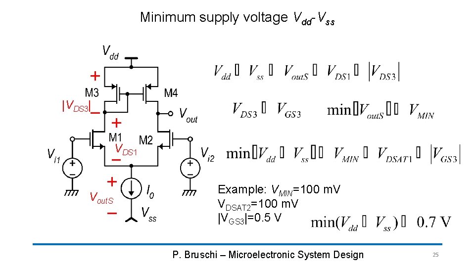
Minimum supply voltage Vdd-Vss |VDS 3| VDS 1 Vout. S Example: VMIN=100 m. V VDSAT 2=100 m. V |VGS 3|=0. 5 V P. Bruschi – Microelectronic System Design 25

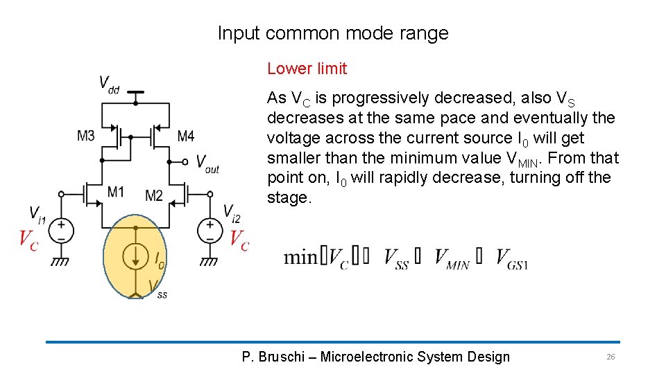
Input common mode range Lower limit As VC is progressively decreased, also VS decreases at the same pace and eventually the voltage across the current source I 0 will get smaller than the minimum value VMIN. From that point on, I 0 will rapidly decrease, turning off the stage. P. Bruschi – Microelectronic System Design 26

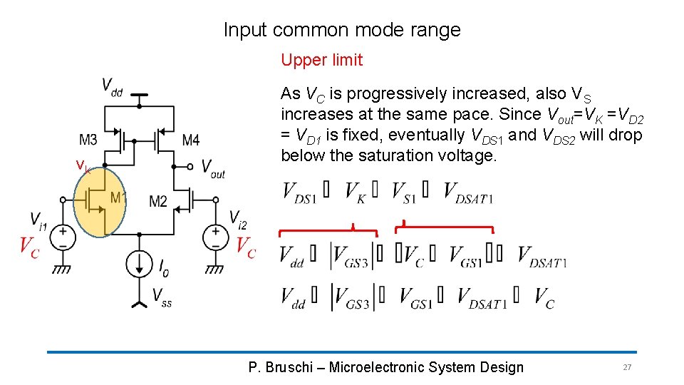
Input common mode range Upper limit vk As VC is progressively increased, also VS increases at the same pace. Since Vout=VK =VD 2 = VD 1 is fixed, eventually VDS 1 and VDS 2 will drop below the saturation voltage. P. Bruschi – Microelectronic System Design 27

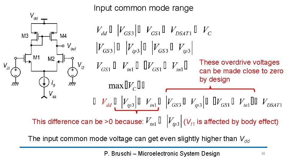
Input common mode range These overdrive voltages can be made close to zero by design This difference can be >0 because: (Vt 1 is affected by body effect) The input common mode voltage can get even slightly higher than Vdd P. Bruschi – Microelectronic System Design 28