CMOS differential amplifier with current mirror load Differential
- Slides: 28

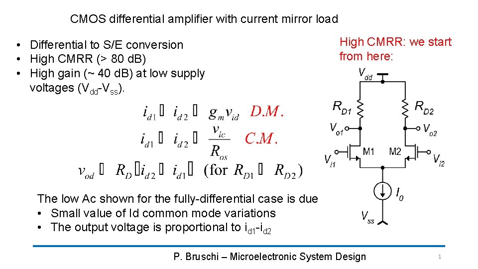
CMOS differential amplifier with current mirror load • Differential to S/E conversion • High CMRR (> 80 d. B) • High gain (~ 40 d. B) at low supply voltages (Vdd-Vss). High CMRR: we start from here: The low Ac shown for the fully-differential case is due • Small value of Id common mode variations • The output voltage is proportional to id 1 -id 2 P. Bruschi – Microelectronic System Design 1

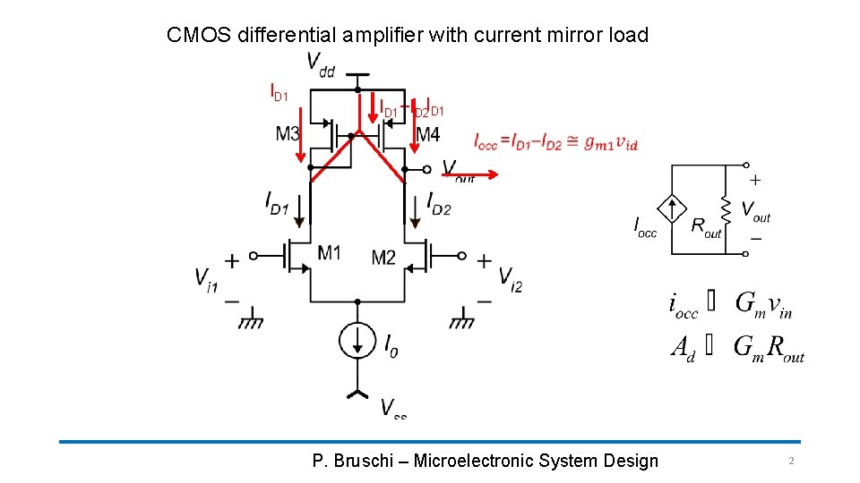
CMOS differential amplifier with current mirror load ID 1+ID 2 ID 1 P. Bruschi – Microelectronic System Design 2

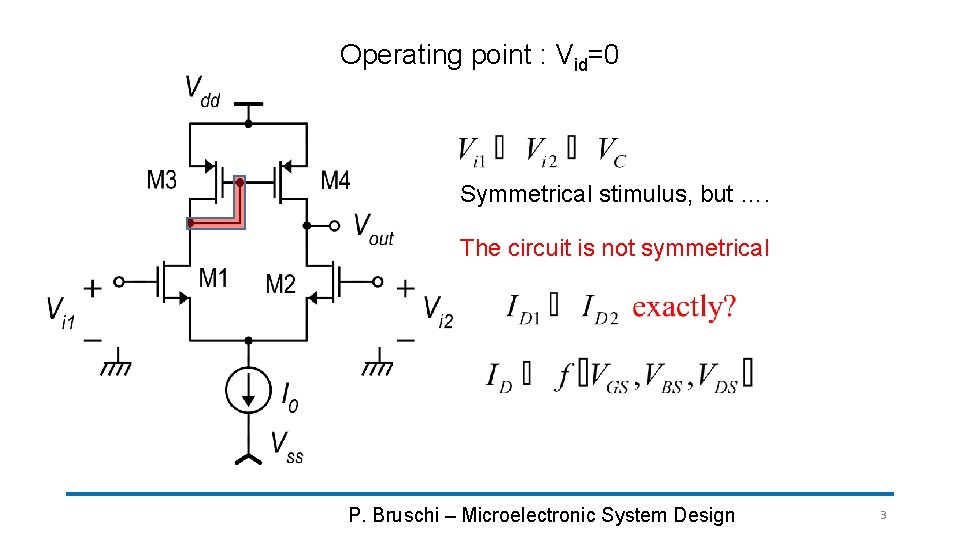
Operating point : Vid=0 Symmetrical stimulus, but …. The circuit is not symmetrical P. Bruschi – Microelectronic System Design 3

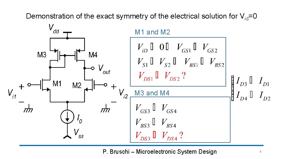
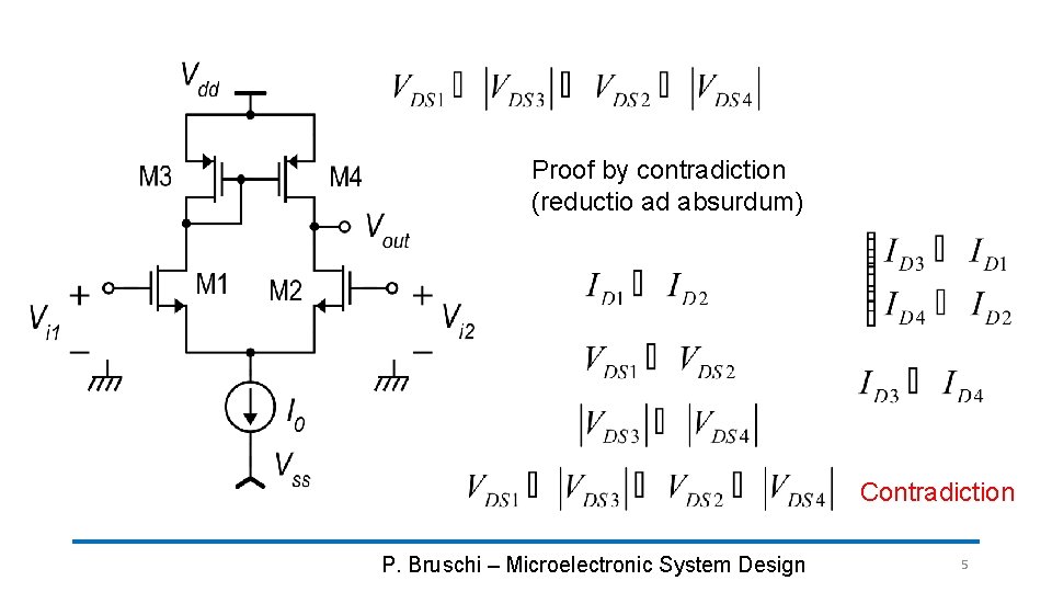
Demonstration of the exact symmetry of the electrical solution for Vid=0 M 1 and M 2 M 3 and M 4 P. Bruschi – Microelectronic System Design 4

Proof by contradiction (reductio ad absurdum) Contradiction P. Bruschi – Microelectronic System Design 5

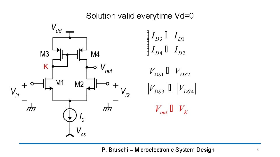
Solution valid everytime Vd=0 K P. Bruschi – Microelectronic System Design 6

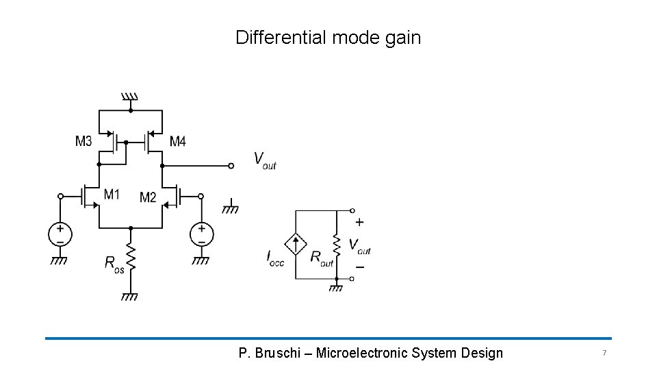
Differential mode gain P. Bruschi – Microelectronic System Design 7

P. Bruschi – Microelectronic System Design 8

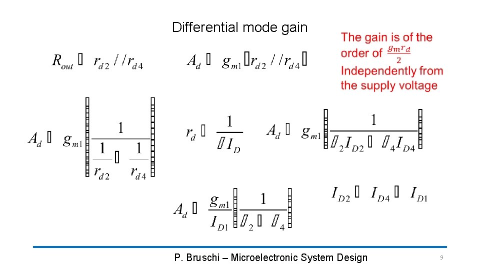
Differential mode gain P. Bruschi – Microelectronic System Design 9

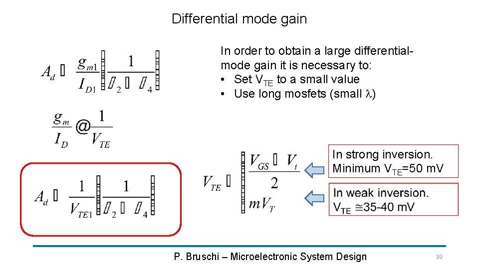
Differential mode gain In order to obtain a large differentialmode gain it is necessary to: • Set VTE to a small value • Use long mosfets (small l) In strong inversion. Minimum VTE=50 m. V P. Bruschi – Microelectronic System Design 10

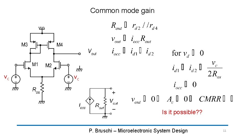
Common mode gain vc vc Is it possible? ? P. Bruschi – Microelectronic System Design 11

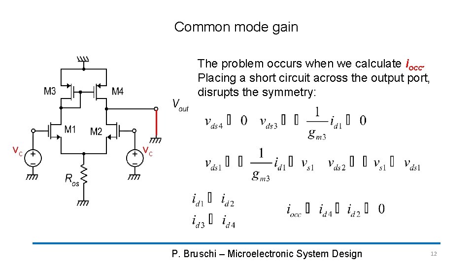
Common mode gain The problem occurs when we calculate iocc. Placing a short circuit across the output port, disrupts the symmetry: vc vc P. Bruschi – Microelectronic System Design 12

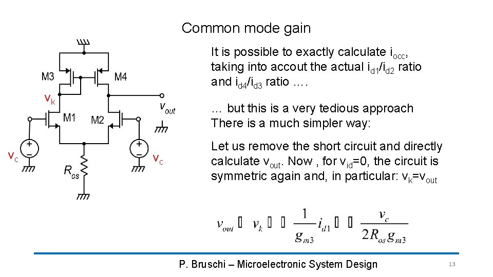
Common mode gain It is possible to exactly calculate iocc, taking into accout the actual id 1/id 2 ratio and id 4/id 3 ratio …. vk vc … but this is a very tedious approach There is a much simpler way: vc Let us remove the short circuit and directly calculate vout. Now , for vid=0, the circuit is symmetric again and, in particular: vk=vout P. Bruschi – Microelectronic System Design 13

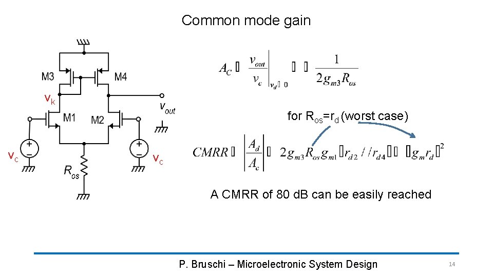
Common mode gain vk for Ros=rd (worst case) vc vc A CMRR of 80 d. B can be easily reached P. Bruschi – Microelectronic System Design 14

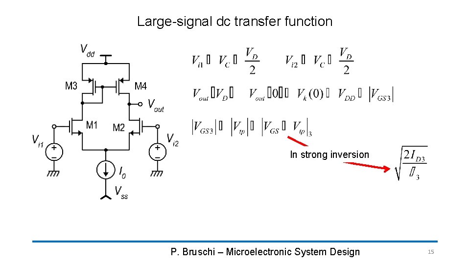
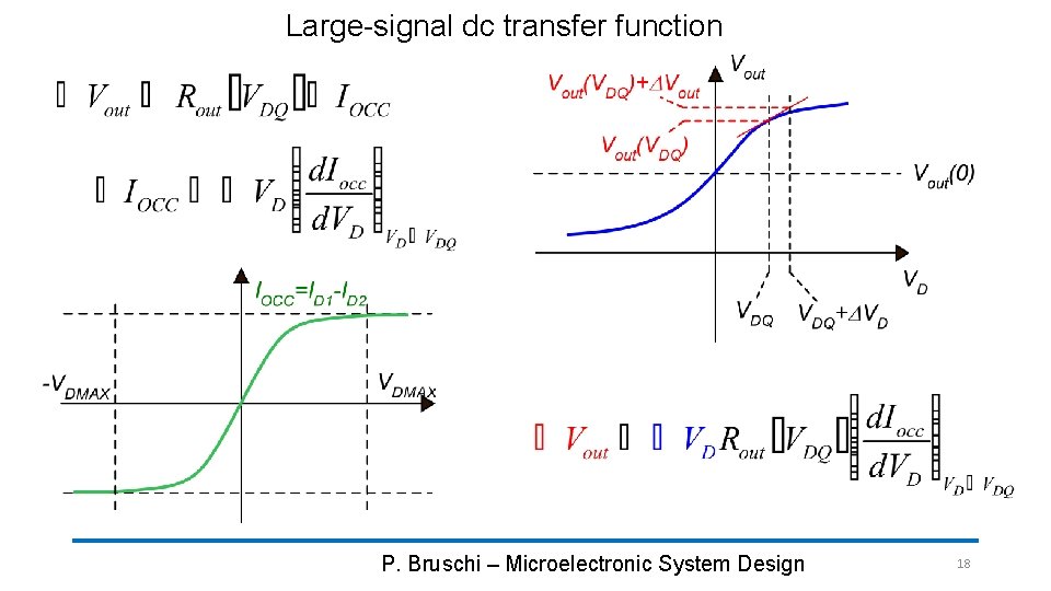
Large-signal dc transfer function In strong inversion P. Bruschi – Microelectronic System Design 15

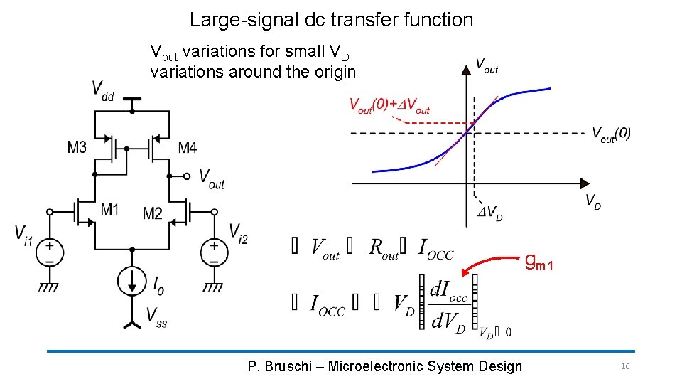
Large-signal dc transfer function Vout variations for small VD variations around the origin gm 1 P. Bruschi – Microelectronic System Design 16

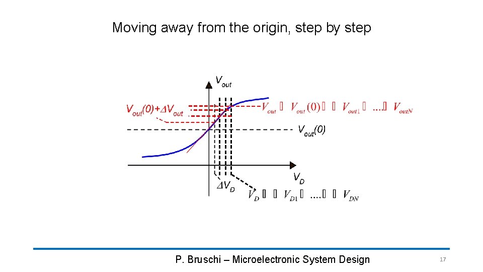
Moving away from the origin, step by step P. Bruschi – Microelectronic System Design 17

Large-signal dc transfer function P. Bruschi – Microelectronic System Design 18

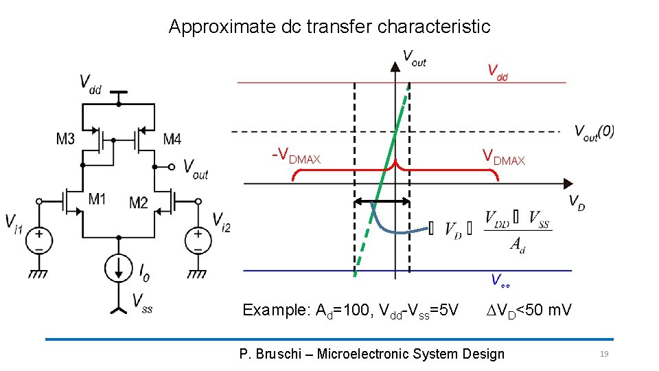
Approximate dc transfer characteristic -VDMAX Example: Ad=100, Vdd-Vss=5 V VDMAX DVD<50 m. V P. Bruschi – Microelectronic System Design 19

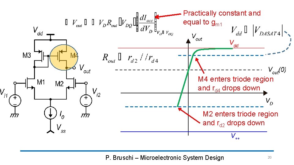
Practically constant and equal to gm 1 M 4 enters triode region and rd 4 drops down M 2 enters triode region and rd 2 drops down P. Bruschi – Microelectronic System Design 20

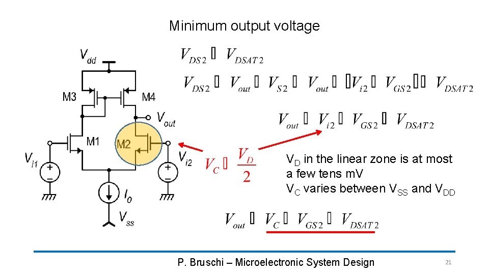
Minimum output voltage VD in the linear zone is at most a few tens m. V VC varies between VSS and VDD P. Bruschi – Microelectronic System Design 21

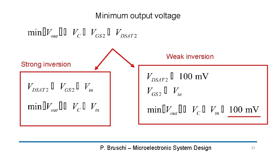
Minimum output voltage Weak inversion Strong inversion P. Bruschi – Microelectronic System Design 22

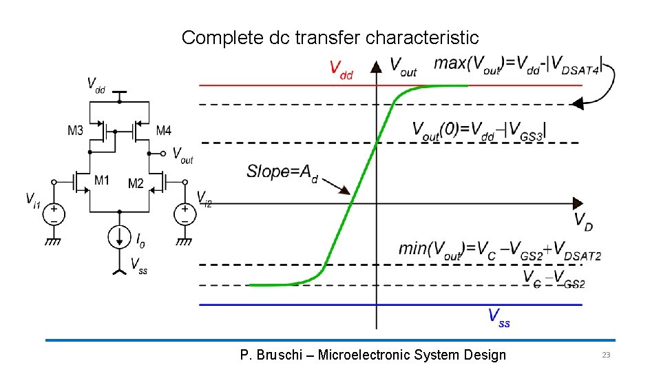
Complete dc transfer characteristic P. Bruschi – Microelectronic System Design 23

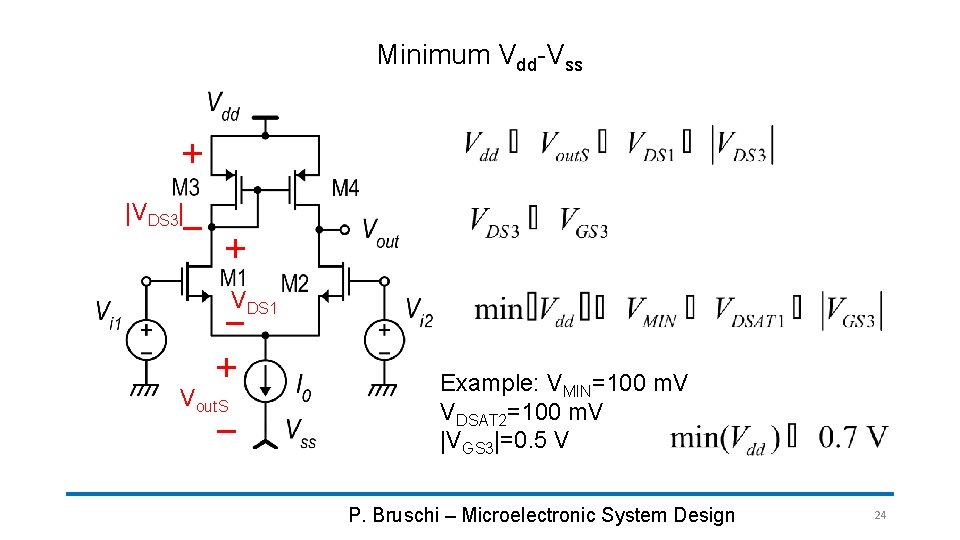
Minimum Vdd-Vss |VDS 3| VDS 1 Vout. S Example: VMIN=100 m. V VDSAT 2=100 m. V |VGS 3|=0. 5 V P. Bruschi – Microelectronic System Design 24

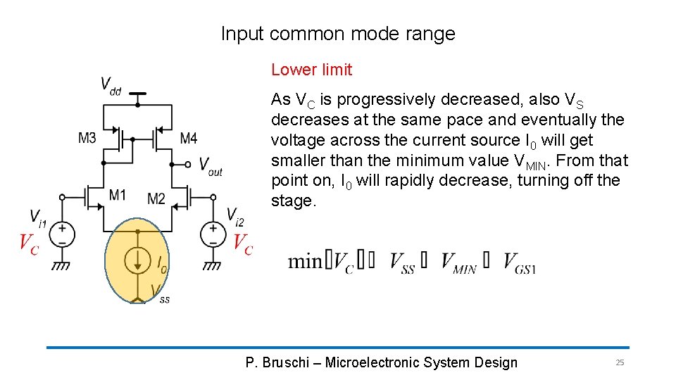
Input common mode range Lower limit As VC is progressively decreased, also VS decreases at the same pace and eventually the voltage across the current source I 0 will get smaller than the minimum value VMIN. From that point on, I 0 will rapidly decrease, turning off the stage. P. Bruschi – Microelectronic System Design 25

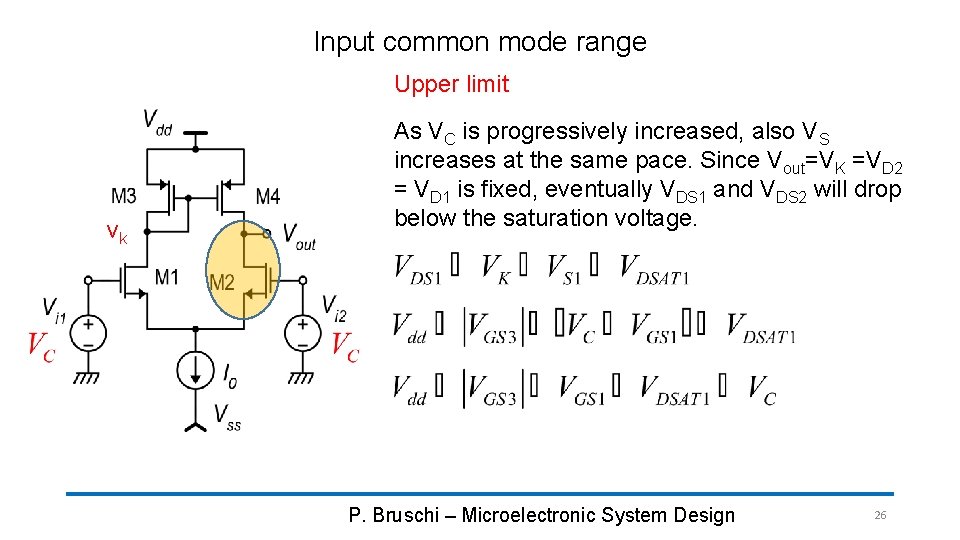
Input common mode range Upper limit vk As VC is progressively increased, also VS increases at the same pace. Since Vout=VK =VD 2 = VD 1 is fixed, eventually VDS 1 and VDS 2 will drop below the saturation voltage. P. Bruschi – Microelectronic System Design 26

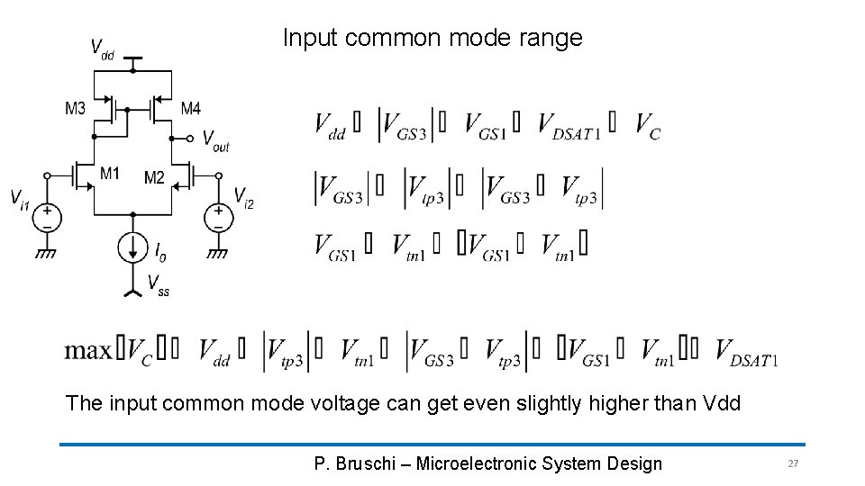
Input common mode range The input common mode voltage can get even slightly higher than Vdd P. Bruschi – Microelectronic System Design 27

P. Bruschi – Microelectronic System Design 28