Chris A Mack Fundamental Principles of Optical Lithography
- Slides: 47

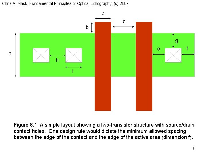
Chris A. Mack, Fundamental Principles of Optical Lithography, (c) 2007 Figure 8. 1 A simple layout showing a two-transistor structure with source/drain contact holes. One design rule would dictate the minimum allowed spacing between the edge of the contact and the edge of the active area (dimension f). 1

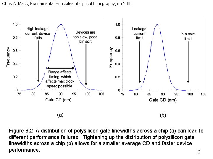
Chris A. Mack, Fundamental Principles of Optical Lithography, (c) 2007 (a) (b) Figure 8. 2 A distribution of polysilicon gate linewidths across a chip (a) can lead to different performance failures. Tightening up the distribution of polysilicon gate linewidths across a chip (b) allows for a smaller average CD and faster device performance. 2

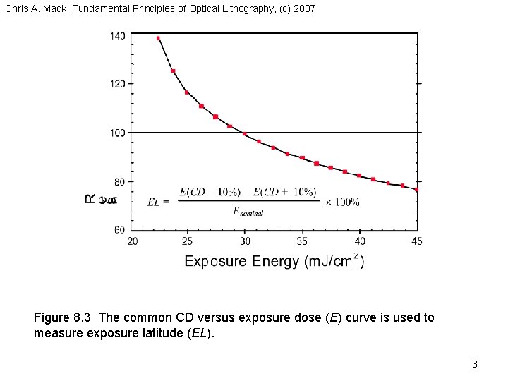
Chris A. Mack, Fundamental Principles of Optical Lithography, (c) 2007 Figure 8. 3 The common CD versus exposure dose (E) curve is used to measure exposure latitude (EL). 3

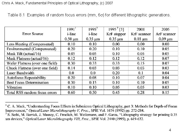
Chris A. Mack, Fundamental Principles of Optical Lithography, (c) 2007 Table 8. 1 Examples of random focus errors (mm, 6 s) for different lithographic generations. 4

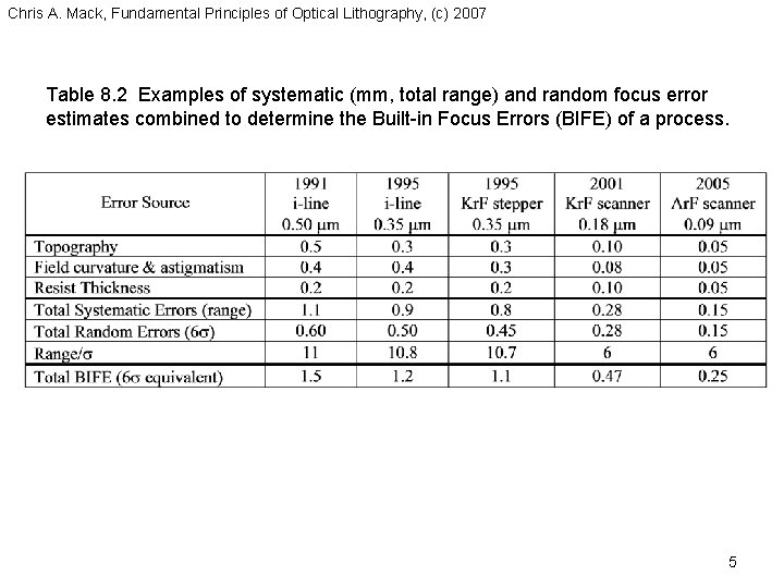
Chris A. Mack, Fundamental Principles of Optical Lithography, (c) 2007 Table 8. 2 Examples of systematic (mm, total range) and random focus error estimates combined to determine the Built-in Focus Errors (BIFE) of a process. 5

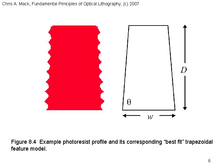
Chris A. Mack, Fundamental Principles of Optical Lithography, (c) 2007 Figure 8. 4 Example photoresist profile and its corresponding “best fit” trapezoidal feature model. 6

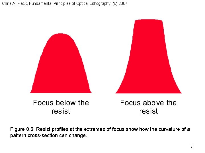
Chris A. Mack, Fundamental Principles of Optical Lithography, (c) 2007 Figure 8. 5 Resist profiles at the extremes of focus show the curvature of a pattern cross-section can change. 7

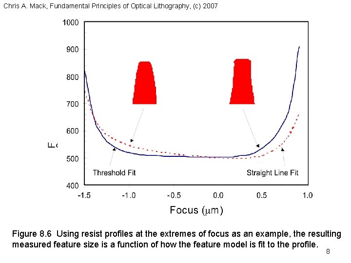
Chris A. Mack, Fundamental Principles of Optical Lithography, (c) 2007 Figure 8. 6 Using resist profiles at the extremes of focus as an example, the resulting measured feature size is a function of how the feature model is fit to the profile. 8

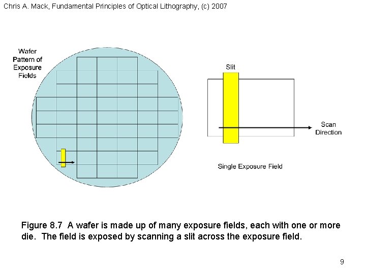
Chris A. Mack, Fundamental Principles of Optical Lithography, (c) 2007 Figure 8. 7 A wafer is made up of many exposure fields, each with one or more die. The field is exposed by scanning a slit across the exposure field. 9

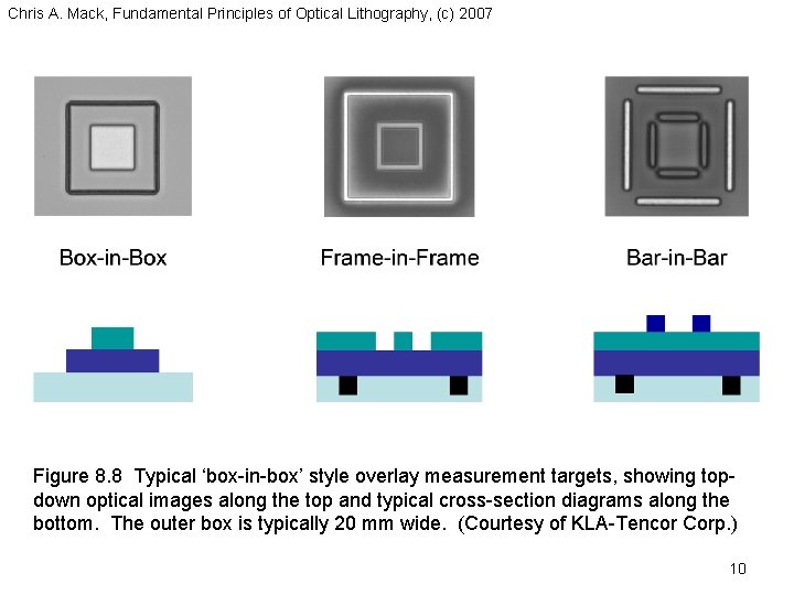
Chris A. Mack, Fundamental Principles of Optical Lithography, (c) 2007 Figure 8. 8 Typical ‘box-in-box’ style overlay measurement targets, showing topdown optical images along the top and typical cross-section diagrams along the bottom. The outer box is typically 20 mm wide. (Courtesy of KLA-Tencor Corp. ) 10

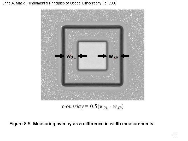
Chris A. Mack, Fundamental Principles of Optical Lithography, (c) 2007 Figure 8. 9 Measuring overlay as a difference in width measurements. 11

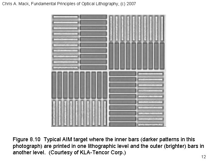
Chris A. Mack, Fundamental Principles of Optical Lithography, (c) 2007 Figure 8. 10 Typical AIM target where the inner bars (darker patterns in this photograph) are printed in one lithographic level and the outer (brighter) bars in another level. (Courtesy of KLA-Tencor Corp. ) 12

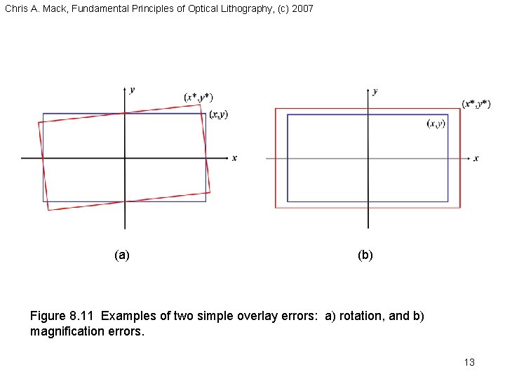
Chris A. Mack, Fundamental Principles of Optical Lithography, (c) 2007 (a) (b) Figure 8. 11 Examples of two simple overlay errors: a) rotation, and b) magnification errors. 13

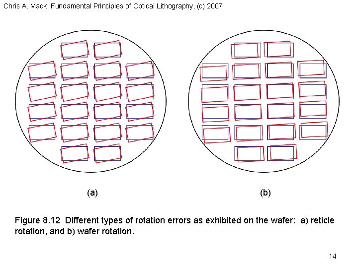
Chris A. Mack, Fundamental Principles of Optical Lithography, (c) 2007 (a) (b) Figure 8. 12 Different types of rotation errors as exhibited on the wafer: a) reticle rotation, and b) wafer rotation. 14

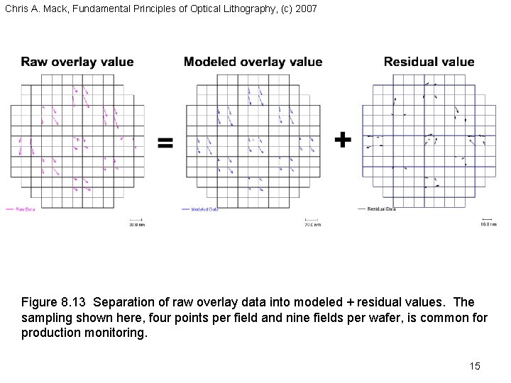
Chris A. Mack, Fundamental Principles of Optical Lithography, (c) 2007 Figure 8. 13 Separation of raw overlay data into modeled + residual values. The sampling shown here, four points per field and nine fields per wafer, is common for production monitoring. 15

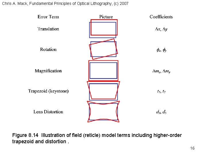
Chris A. Mack, Fundamental Principles of Optical Lithography, (c) 2007 Figure 8. 14 Illustration of field (reticle) model terms including higher-order trapezoid and distortion. 16

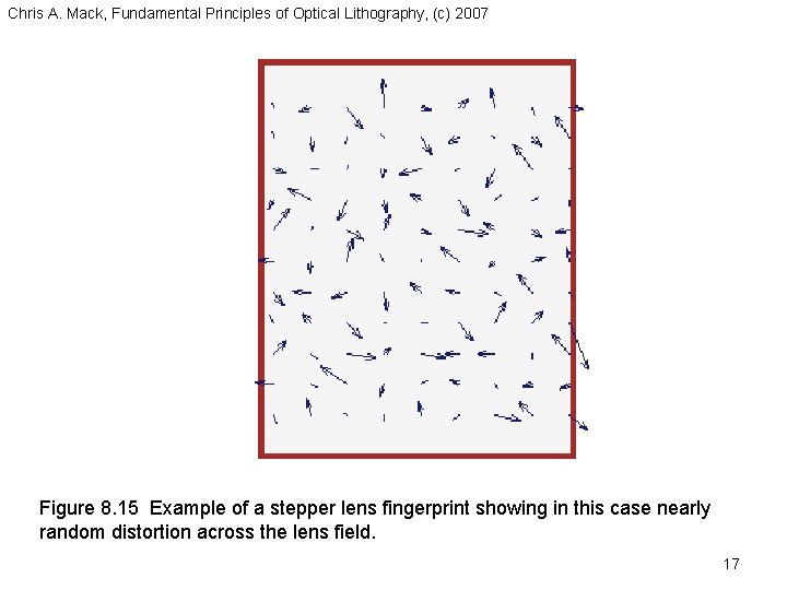
Chris A. Mack, Fundamental Principles of Optical Lithography, (c) 2007 Figure 8. 15 Example of a stepper lens fingerprint showing in this case nearly random distortion across the lens field. 17

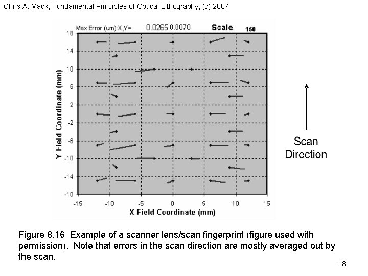
Chris A. Mack, Fundamental Principles of Optical Lithography, (c) 2007 Figure 8. 16 Example of a scanner lens/scan fingerprint (figure used with permission). Note that errors in the scan direction are mostly averaged out by the scan. 18

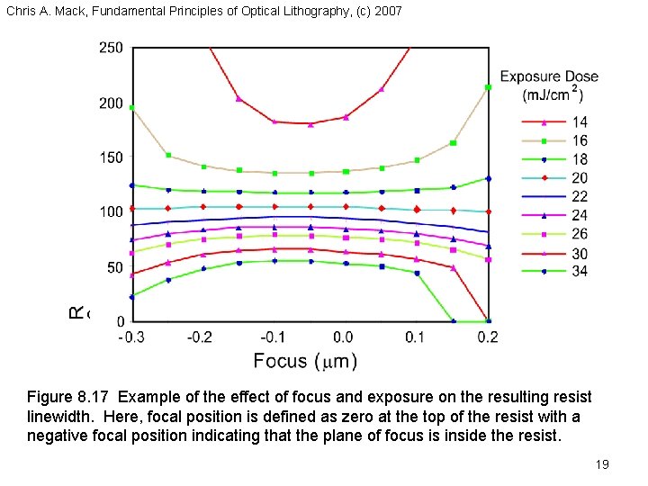
Chris A. Mack, Fundamental Principles of Optical Lithography, (c) 2007 Figure 8. 17 Example of the effect of focus and exposure on the resulting resist linewidth. Here, focal position is defined as zero at the top of the resist with a negative focal position indicating that the plane of focus is inside the resist. 19

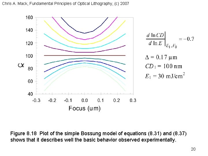
Chris A. Mack, Fundamental Principles of Optical Lithography, (c) 2007 Figure 8. 18 Plot of the simple Bossung model of equations (8. 31) and (8. 37) shows that it describes well the basic behavior observed experimentally. 20

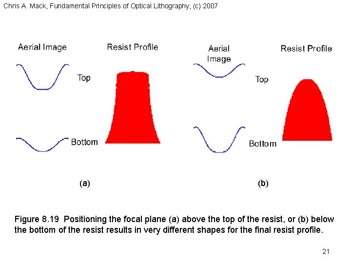
Chris A. Mack, Fundamental Principles of Optical Lithography, (c) 2007 (a) (b) Figure 8. 19 Positioning the focal plane (a) above the top of the resist, or (b) below the bottom of the resist results in very different shapes for the final resist profile. 21

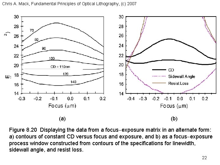
Chris A. Mack, Fundamental Principles of Optical Lithography, (c) 2007 (a) (b) Figure 8. 20 Displaying the data from a focus exposure matrix in an alternate form: a) contours of constant CD versus focus and exposure, and b) as a focus exposure process window constructed from contours of the specifications for linewidth, sidewall angle, and resist loss. 22

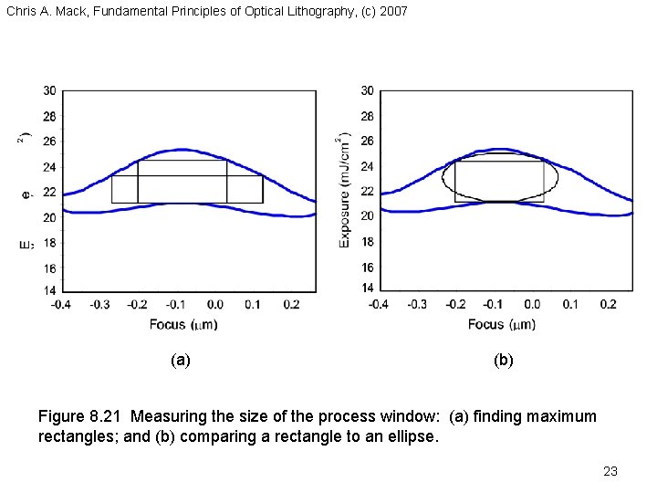
Chris A. Mack, Fundamental Principles of Optical Lithography, (c) 2007 (a) (b) Figure 8. 21 Measuring the size of the process window: (a) finding maximum rectangles; and (b) comparing a rectangle to an ellipse. 23

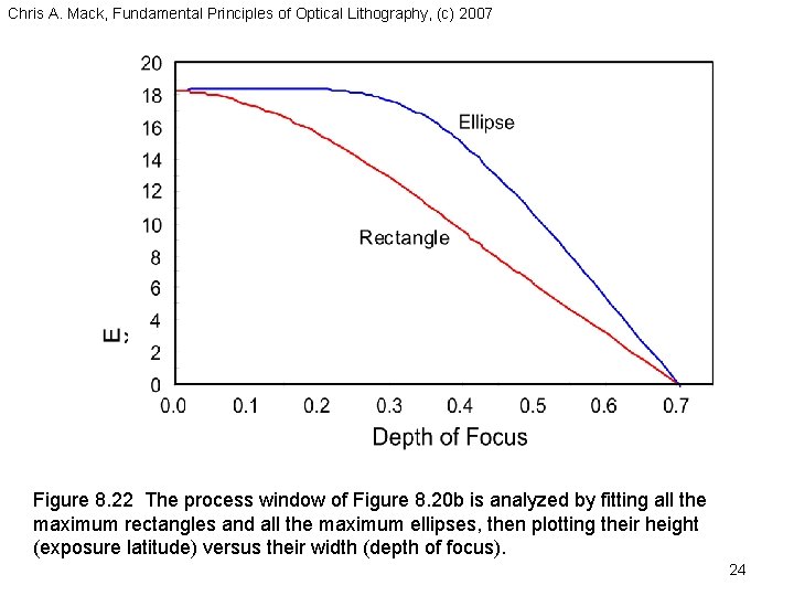
Chris A. Mack, Fundamental Principles of Optical Lithography, (c) 2007 Figure 8. 22 The process window of Figure 8. 20 b is analyzed by fitting all the maximum rectangles and all the maximum ellipses, then plotting their height (exposure latitude) versus their width (depth of focus). 24

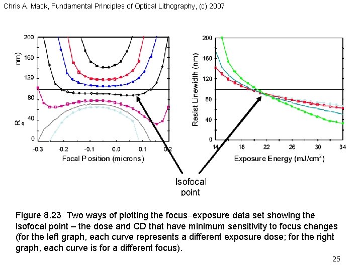
Chris A. Mack, Fundamental Principles of Optical Lithography, (c) 2007 Figure 8. 23 Two ways of plotting the focus exposure data set showing the isofocal point – the dose and CD that have minimum sensitivity to focus changes (for the left graph, each curve represents a different exposure dose; for the right graph, each curve is for a different focus). 25

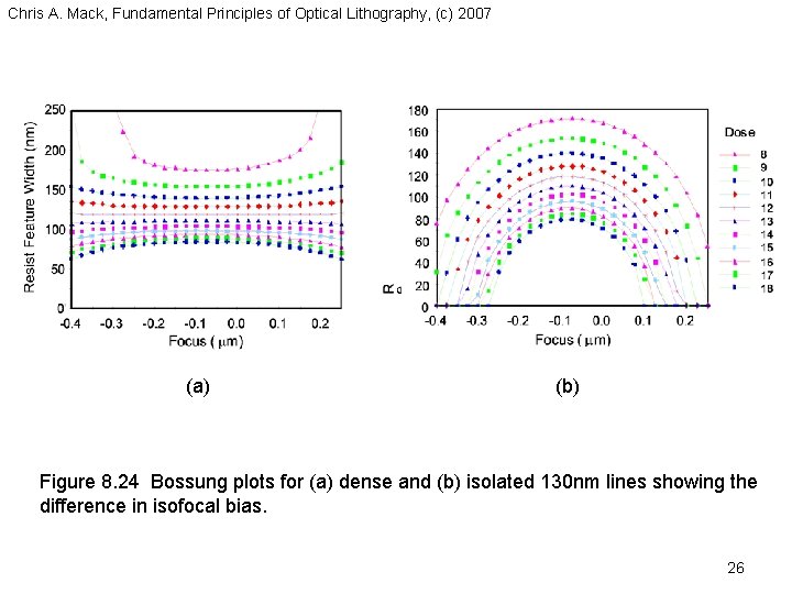
Chris A. Mack, Fundamental Principles of Optical Lithography, (c) 2007 (a) (b) Figure 8. 24 Bossung plots for (a) dense and (b) isolated 130 nm lines showing the difference in isofocal bias. 26

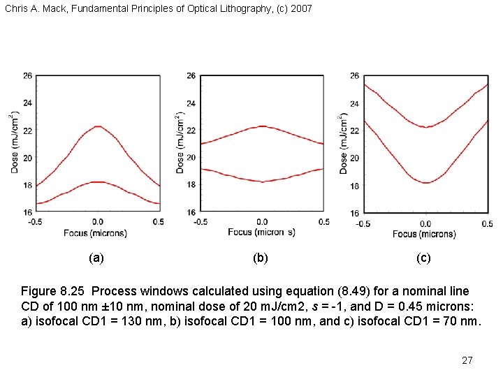
Chris A. Mack, Fundamental Principles of Optical Lithography, (c) 2007 (a) (b) (c) Figure 8. 25 Process windows calculated using equation (8. 49) for a nominal line CD of 100 nm ± 10 nm, nominal dose of 20 m. J/cm 2, s = -1, and D = 0. 45 microns: a) isofocal CD 1 = 130 nm, b) isofocal CD 1 = 100 nm, and c) isofocal CD 1 = 70 nm. 27

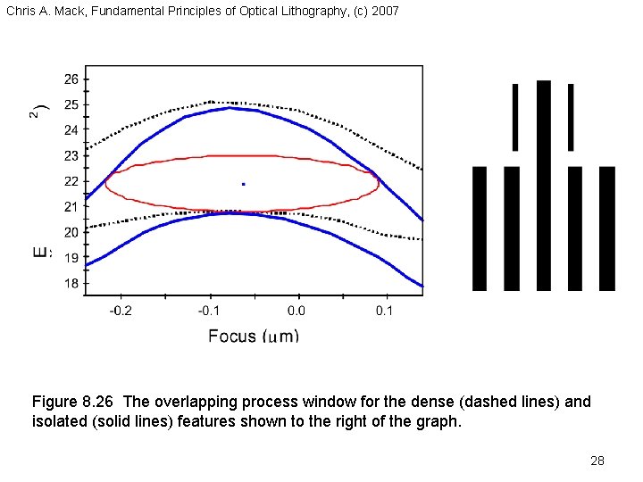
Chris A. Mack, Fundamental Principles of Optical Lithography, (c) 2007 Figure 8. 26 The overlapping process window for the dense (dashed lines) and isolated (solid lines) features shown to the right of the graph. 28

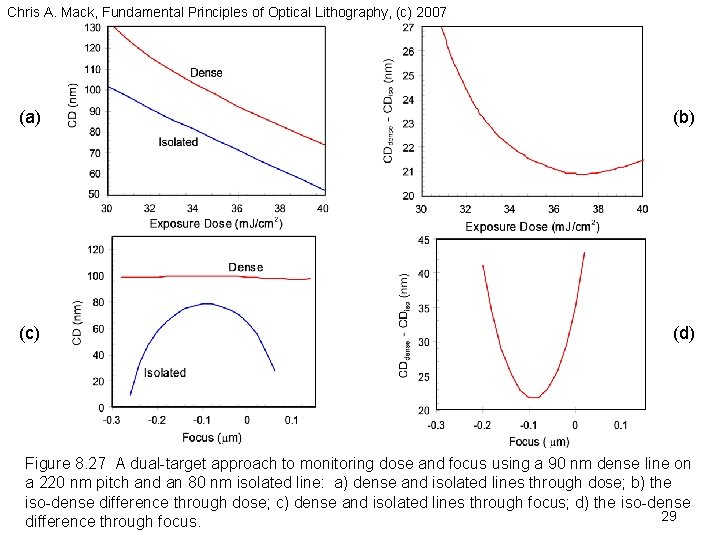
Chris A. Mack, Fundamental Principles of Optical Lithography, (c) 2007 (a) (b) (c) (d) Figure 8. 27 A dual-target approach to monitoring dose and focus using a 90 nm dense line on a 220 nm pitch and an 80 nm isolated line: a) dense and isolated lines through dose; b) the iso-dense difference through dose; c) dense and isolated lines through focus; d) the iso-dense 29 difference through focus.

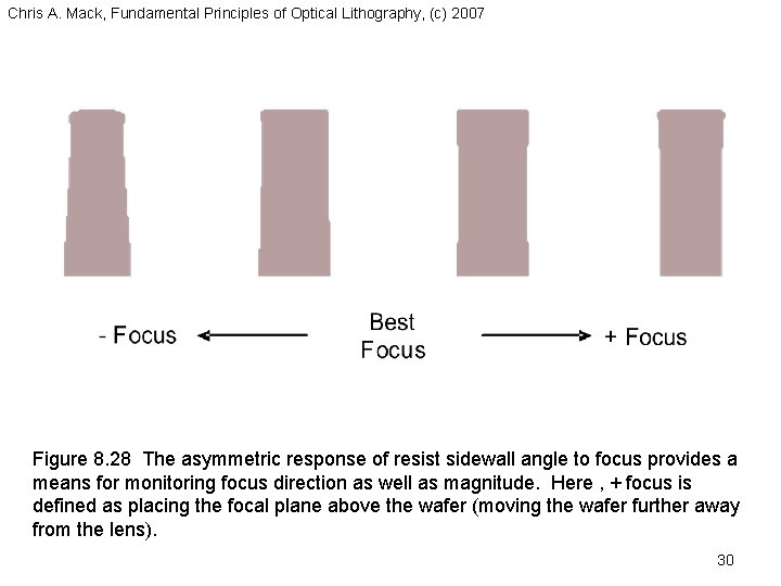
Chris A. Mack, Fundamental Principles of Optical Lithography, (c) 2007 Figure 8. 28 The asymmetric response of resist sidewall angle to focus provides a means for monitoring focus direction as well as magnitude. Here , + focus is defined as placing the focal plane above the wafer (moving the wafer further away from the lens). 30

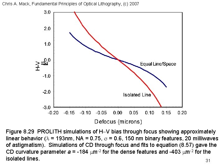
Chris A. Mack, Fundamental Principles of Optical Lithography, (c) 2007 Figure 8. 29 PROLITH simulations of H V bias through focus showing approximately linear behavior (l = 193 nm, NA = 0. 75, s = 0. 6, 150 nm binary features, 20 milliwaves of astigmatism). Simulations of CD through focus and fits to equation (8. 57) gave the CD curvature parameter a = -184 mm-2 for the dense features and -403 mm-2 for the isolated lines. 31

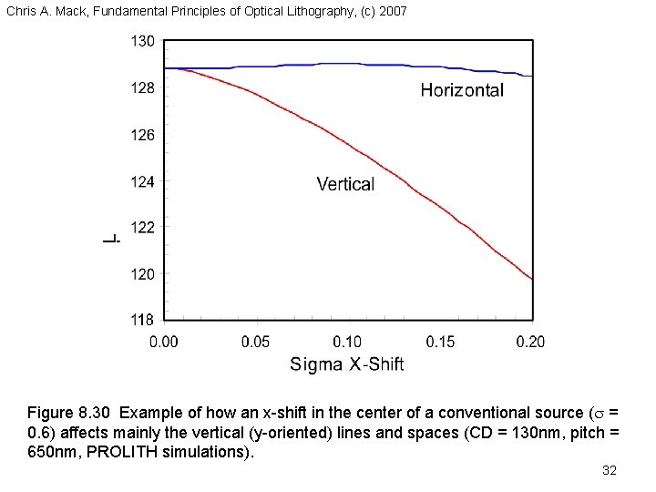
Chris A. Mack, Fundamental Principles of Optical Lithography, (c) 2007 Figure 8. 30 Example of how an x-shift in the center of a conventional source (s = 0. 6) affects mainly the vertical (y-oriented) lines and spaces (CD = 130 nm, pitch = 650 nm, PROLITH simulations). 32

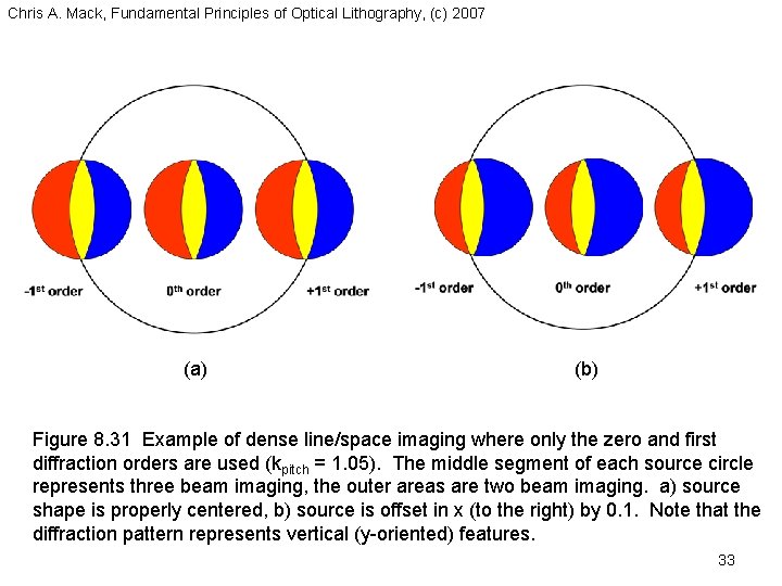
Chris A. Mack, Fundamental Principles of Optical Lithography, (c) 2007 (a) (b) Figure 8. 31 Example of dense line/space imaging where only the zero and first diffraction orders are used (kpitch = 1. 05). The middle segment of each source circle represents three beam imaging, the outer areas are two beam imaging. a) source shape is properly centered, b) source is offset in x (to the right) by 0. 1. Note that the diffraction pattern represents vertical (y-oriented) features. 33

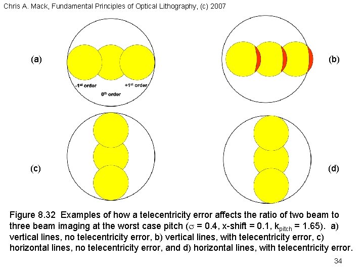
Chris A. Mack, Fundamental Principles of Optical Lithography, (c) 2007 (a) (b) (c) (d) Figure 8. 32 Examples of how a telecentricity error affects the ratio of two beam to three beam imaging at the worst case pitch (s = 0. 4, x-shift = 0. 1, kpitch = 1. 65). a) vertical lines, no telecentricity error, b) vertical lines, with telecentricity error, c) horizontal lines, no telecentricity error, and d) horizontal lines, with telecentricity error. 34

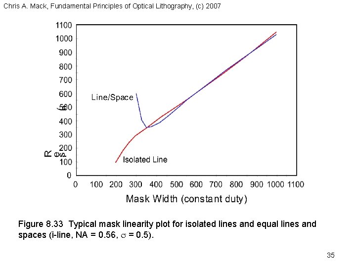
Chris A. Mack, Fundamental Principles of Optical Lithography, (c) 2007 Figure 8. 33 Typical mask linearity plot for isolated lines and equal lines and spaces (i-line, NA = 0. 56, s = 0. 5). 35

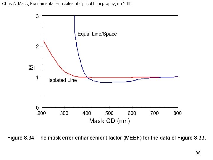
Chris A. Mack, Fundamental Principles of Optical Lithography, (c) 2007 Figure 8. 34 The mask error enhancement factor (MEEF) for the data of Figure 8. 33. 36

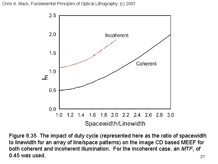
Chris A. Mack, Fundamental Principles of Optical Lithography, (c) 2007 Figure 8. 35 The impact of duty cycle (represented here as the ratio of spacewidth to linewidth for an array of line/space patterns) on the image CD based MEEF for both coherent and incoherent illumination. For the incoherent case, an MTF 1 of 0. 45 was used. 37

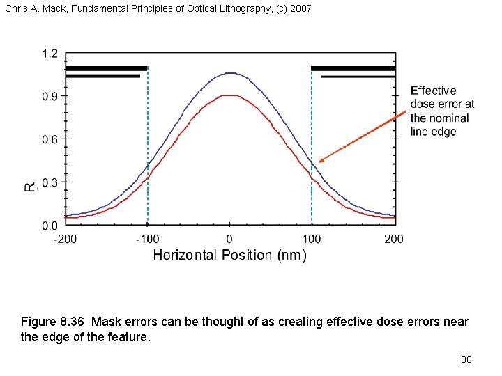
Chris A. Mack, Fundamental Principles of Optical Lithography, (c) 2007 Figure 8. 36 Mask errors can be thought of as creating effective dose errors near the edge of the feature. 38

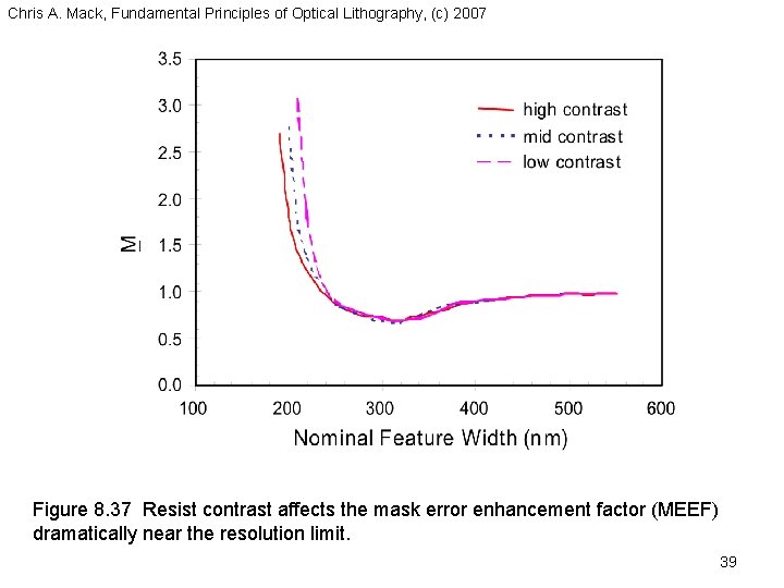
Chris A. Mack, Fundamental Principles of Optical Lithography, (c) 2007 Figure 8. 37 Resist contrast affects the mask error enhancement factor (MEEF) dramatically near the resolution limit. 39

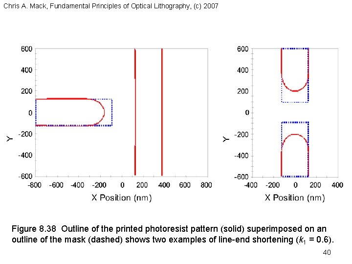
Chris A. Mack, Fundamental Principles of Optical Lithography, (c) 2007 Figure 8. 38 Outline of the printed photoresist pattern (solid) superimposed on an outline of the mask (dashed) shows two examples of line-end shortening (k 1 = 0. 6). 40

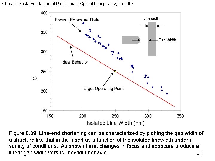
Chris A. Mack, Fundamental Principles of Optical Lithography, (c) 2007 Figure 8. 39 Line-end shortening can be characterized by plotting the gap width of a structure like that in the insert as a function of the isolated linewidth under a variety of conditions. As shown here, changes in focus and exposure produce a linear gap width versus linewidth behavior. 41

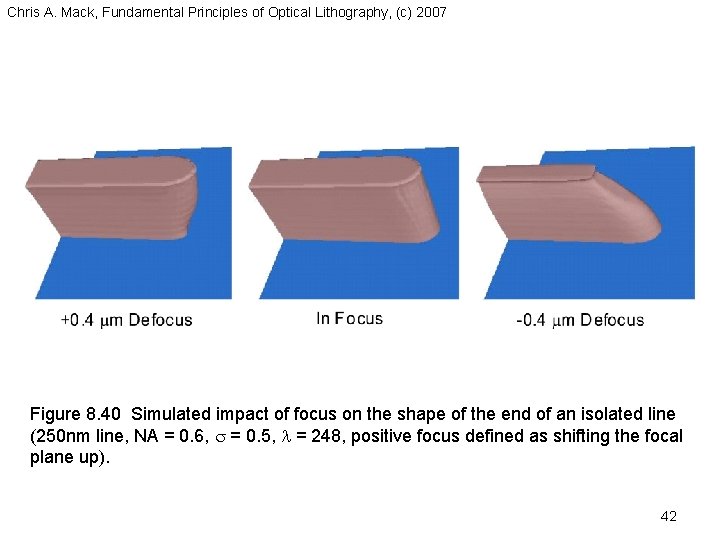
Chris A. Mack, Fundamental Principles of Optical Lithography, (c) 2007 Figure 8. 40 Simulated impact of focus on the shape of the end of an isolated line (250 nm line, NA = 0. 6, s = 0. 5, l = 248, positive focus defined as shifting the focal plane up). 42

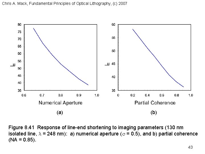
Chris A. Mack, Fundamental Principles of Optical Lithography, (c) 2007 (a) (b) Figure 8. 41 Response of line-end shortening to imaging parameters (130 nm isolated line, l = 248 nm): a) numerical aperture (s = 0. 5), and b) partial coherence (NA = 0. 85). 43

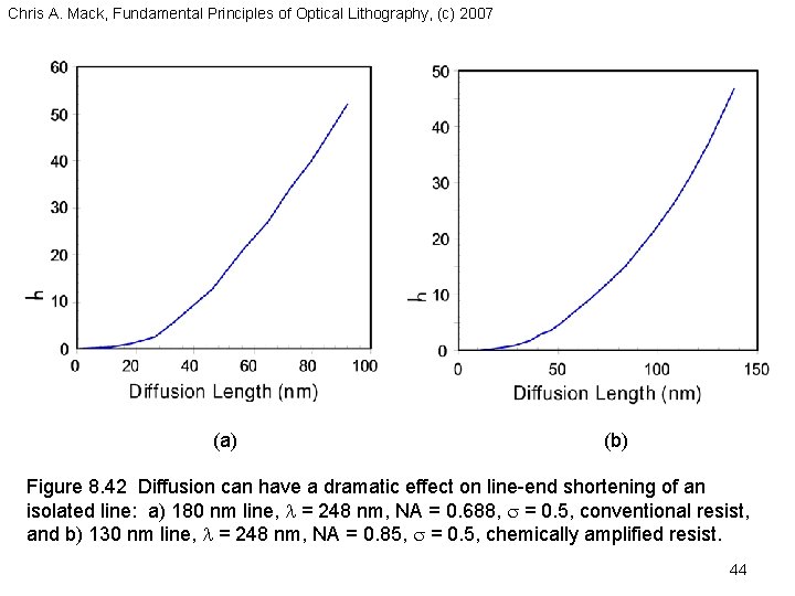
Chris A. Mack, Fundamental Principles of Optical Lithography, (c) 2007 (a) (b) Figure 8. 42 Diffusion can have a dramatic effect on line-end shortening of an isolated line: a) 180 nm line, l = 248 nm, NA = 0. 688, s = 0. 5, conventional resist, and b) 130 nm line, l = 248 nm, NA = 0. 85, s = 0. 5, chemically amplified resist. 44

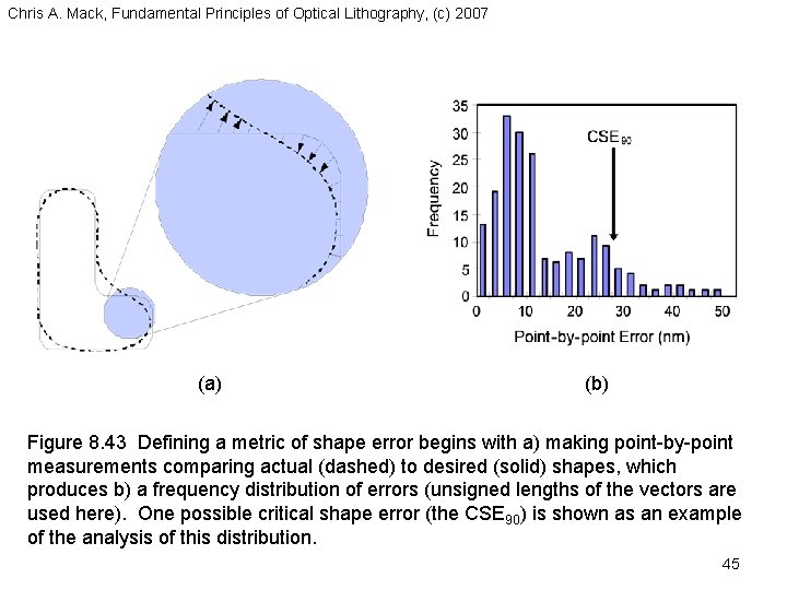
Chris A. Mack, Fundamental Principles of Optical Lithography, (c) 2007 (a) (b) Figure 8. 43 Defining a metric of shape error begins with a) making point-by-point measurements comparing actual (dashed) to desired (solid) shapes, which produces b) a frequency distribution of errors (unsigned lengths of the vectors are used here). One possible critical shape error (the CSE 90) is shown as an example of the analysis of this distribution. 45

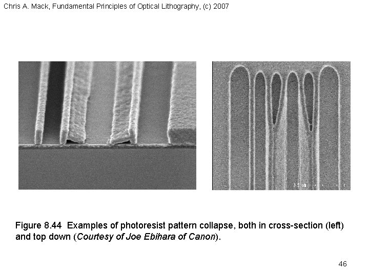
Chris A. Mack, Fundamental Principles of Optical Lithography, (c) 2007 Figure 8. 44 Examples of photoresist pattern collapse, both in cross-section (left) and top down (Courtesy of Joe Ebihara of Canon). 46

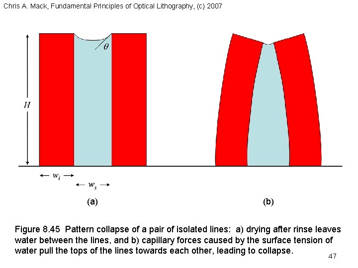
Chris A. Mack, Fundamental Principles of Optical Lithography, (c) 2007 (a) (b) Figure 8. 45 Pattern collapse of a pair of isolated lines: a) drying after rinse leaves water between the lines, and b) capillary forces caused by the surface tension of water pull the tops of the lines towards each other, leading to collapse. 47