LITHOGRAPHY Lithography is the process of imprinting a


 which can be classified as")


- Slides: 16
LITHOGRAPHY Lithography is the process of imprinting a geometric pattern from a mask onto a thin layer of material called a resist which is a radiation sensitive polymer. • Process to fabricate a certain structure : - First a resist is spin-coated or sprayed onto the wafer. - A mask is then placed above the resist. - A radiation is transmitted through the "clear" parts of the mask. - The structure pattern of opaque material (mask material) blocks some of the radiation. - The radiation is used to change the solubility of the resist in a known solvent.
• The pattern transfer process is accomplished by using a lithographic exposure tool which emits radiation. • The performance of the radiation tool is determined by three parameters : - Resolution : the minimum feature size that can be transferred with high fidelity to a resist film on the surface of the wafer. - Registration : is a measure of how accurately patterns on successive masks can be aligned with respect to previously defined patterns on a wafer. - Throughput : is the number of wafers that can be exposed per hour for a given mask level. • Depending on resolution different types of radiation may be employed in lithography ; these radiations include ultraviolet (UV) light (optical lithography), electrons, x-ray, and ions.
Optical Lithography - It uses DUV and laser radiation ( l ~ 0. 2 to 0. 4 mm). - Typical parameters are : Resolution ~ 100 nm – 1 mm. Registration ~ 50 nm. Throughput ~ 50 to 100 wafers per hour. - Optical lithography is the common method in N/MEMS. X-ray, E-Beam, and Ion-Beam Lithographies - Typical parameters for both lithographies are : Resolution ~ 30 - 50 nm. Registration ~ 20 nm. - These lithographies require complicated masks.
Mask Formation • For a certain device, a large composite layout of the mask set is first drawn. • This layout is typically a hundred to a few thousands times the final size. • The composite layout is then broken into mask levels that correspond to a particular process sequence such as isolation region on one level, the metallization on another, etc. • Artwork is drawn for each masking level, the artwork is reduced to 10 x (ten times) glass reticle by using a reduction camera, and the final mask is made from the 10 x reticle using a special projection printing system. • The choice of mask material depends on the desired resolution. For feature sizes of 5 mm or larger, masks are made from glass plates covered with a soft surface material such as emulsion. For smaller feature sizes, masks are made from glass covered with hard surface materials such as chromium or iron oxide.
Mask Formation : Schematic of a Photomask-Making Machine • • • The information containing the geometrical features corresponding to a particular mask is electronically entered with the aid of a layout editor system. The geometric layout is then broken down into rectangular regions of fixed dimensions. The fractured mask data is stored on a tape, which is transferred to mask-making machine. A reticle mask plate consisting of glass plate coated with a light blocking material (e. g. , Cr) and a photoresist coating is placed on the positioning stage. The tape data are then read by the mask maker and specifies the position of the stage and the aperture of the shutter blades.
Resist A resist is a radiation-sensitive material (usually polymer) which can be classified as positive or negative, depending on how it responds to radiation. Positive Resist It is rendered soluble in a developer when exposed to radiation. Therefore after exposure to radiation a positive resist can be easily removed in the development process. The net effect is that the patterns formed (also called images) in the positive resist are the same as those on the mask. Negative Resist It becomes less soluble in a developer when exposed to radiation. The patterns formed in a negative resist are the reverse of the mask patterns.
Spin Casting : A Method Used For Resist Layer Formation • • • Spin casting is a process by which one can deposit uniform films of various liquids by spinning them onto a wafer. The thickness of the spin-on material, l. R , is Typical spin speeds are in the range 1000 to 10, 000 rpm to give material thicknesses in the range 1 to 0. 5 mm.
Spin-On Materials
Photo-resist • The response curves describe the percent resist remaining after exposure and development versus the exposure energy. • Positive Resist : the resist has a finite solubility in its developer, even without exposure to radiation. As the exposure energy increases, the solubility increases until, at some threshold energy, ET, the resist becomes completely soluble.
Commercially Available Resists
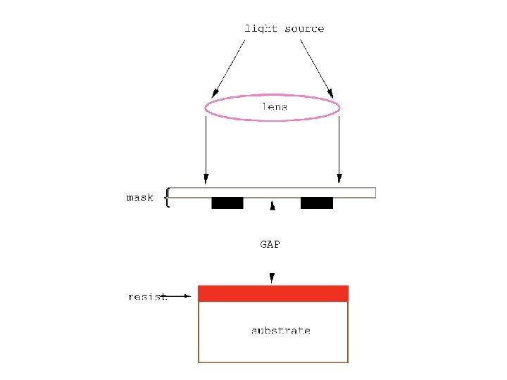
Optical Lithography : Shadow Printing • • • Contact printing : mask and wafer in direct contact with each other. The intimate contact between wafer and mask offers very high resolution (~ 1 mm). However contact printing may cause mask damage caused by particles from wafer surface. Proximity printing : mask and wafer in close proximity [ a small gap (g) ~ 10 to 50 mm]. The small gap results in diffraction which limits resolution to ~ 2 to 5 mm range. Minimum line-width (l) that can be printed in shadow printing is
Optical Lithography : Projection Printing • • • To avoid the mask damage problem associated with shadow printing, projection printing exposure tools are used to project image of the mask patterns onto a resist-coated wafer many centimeters away from the mask. To increase resolution, only a small portion of the mask is exposed at a time. A narrow, arc-shaped image field ~ 1 mm in width serially transfers the slit image of the mask onto the wafer. Typical resolution ~ 1 mm.
Pattern Transfer
Pattern Transfer : Positive Resist vs Negative Resist
Pattern Transfer : Lift-Off Technique • It uses a positive resist to form the resist pattern on the substrate. • The film is deposited over the resist and the substrate ; the film thickness must be smaller than that of the resist. • The lift-off technique is capable of high resolution and is used extensively for discrete devices.